EP0997946B1 - Deep divot in shallow trench isolation for a buried-channel PFET - Google Patents
Deep divot in shallow trench isolation for a buried-channel PFET Download PDFInfo
- Publication number
- EP0997946B1 EP0997946B1 EP99308122A EP99308122A EP0997946B1 EP 0997946 B1 EP0997946 B1 EP 0997946B1 EP 99308122 A EP99308122 A EP 99308122A EP 99308122 A EP99308122 A EP 99308122A EP 0997946 B1 EP0997946 B1 EP 0997946B1
- Authority
- EP
- European Patent Office
- Prior art keywords
- wells
- divots
- adjacent
- depth
- channel
- Prior art date
- Legal status (The legal status is an assumption and is not a legal conclusion. Google has not performed a legal analysis and makes no representation as to the accuracy of the status listed.)
- Expired - Lifetime
Links
Images



Classifications
-
- H—ELECTRICITY
- H10—SEMICONDUCTOR DEVICES; ELECTRIC SOLID-STATE DEVICES NOT OTHERWISE PROVIDED FOR
- H10D—INORGANIC ELECTRIC SEMICONDUCTOR DEVICES
- H10D30/00—Field-effect transistors [FET]
- H10D30/60—Insulated-gate field-effect transistors [IGFET]
-
- H—ELECTRICITY
- H10—SEMICONDUCTOR DEVICES; ELECTRIC SOLID-STATE DEVICES NOT OTHERWISE PROVIDED FOR
- H10D—INORGANIC ELECTRIC SEMICONDUCTOR DEVICES
- H10D84/00—Integrated devices formed in or on semiconductor substrates that comprise only semiconducting layers, e.g. on Si wafers or on GaAs-on-Si wafers
- H10D84/80—Integrated devices formed in or on semiconductor substrates that comprise only semiconducting layers, e.g. on Si wafers or on GaAs-on-Si wafers characterised by the integration of at least one component covered by groups H10D12/00 or H10D30/00, e.g. integration of IGFETs
- H10D84/82—Integrated devices formed in or on semiconductor substrates that comprise only semiconducting layers, e.g. on Si wafers or on GaAs-on-Si wafers characterised by the integration of at least one component covered by groups H10D12/00 or H10D30/00, e.g. integration of IGFETs of only field-effect components
- H10D84/83—Integrated devices formed in or on semiconductor substrates that comprise only semiconducting layers, e.g. on Si wafers or on GaAs-on-Si wafers characterised by the integration of at least one component covered by groups H10D12/00 or H10D30/00, e.g. integration of IGFETs of only field-effect components of only insulated-gate FETs [IGFET]
- H10D84/85—Complementary IGFETs, e.g. CMOS
- H10D84/859—Complementary IGFETs, e.g. CMOS comprising both N-type and P-type wells, e.g. twin-tub
-
- H—ELECTRICITY
- H10—SEMICONDUCTOR DEVICES; ELECTRIC SOLID-STATE DEVICES NOT OTHERWISE PROVIDED FOR
- H10W—GENERIC PACKAGES, INTERCONNECTIONS, CONNECTORS OR OTHER CONSTRUCTIONAL DETAILS OF DEVICES COVERED BY CLASS H10
- H10W10/00—Isolation regions in semiconductor bodies between components of integrated devices
- H10W10/01—Manufacture or treatment
- H10W10/011—Manufacture or treatment of isolation regions comprising dielectric materials
- H10W10/014—Manufacture or treatment of isolation regions comprising dielectric materials using trench refilling with dielectric materials, e.g. shallow trench isolations
- H10W10/0148—Manufacture or treatment of isolation regions comprising dielectric materials using trench refilling with dielectric materials, e.g. shallow trench isolations comprising introducing impurities in side walls or bottom walls of trenches, e.g. for forming channel stoppers
-
- H—ELECTRICITY
- H10—SEMICONDUCTOR DEVICES; ELECTRIC SOLID-STATE DEVICES NOT OTHERWISE PROVIDED FOR
- H10W—GENERIC PACKAGES, INTERCONNECTIONS, CONNECTORS OR OTHER CONSTRUCTIONAL DETAILS OF DEVICES COVERED BY CLASS H10
- H10W10/00—Isolation regions in semiconductor bodies between components of integrated devices
- H10W10/10—Isolation regions comprising dielectric materials
- H10W10/17—Isolation regions comprising dielectric materials formed using trench refilling with dielectric materials, e.g. shallow trench isolations
Definitions
- the present invention generally relates to controlling the amount of gate wrap-around within metal oxide semiconductor field effect transistors by adjusting the depth of divots within the shallow trench isolation regions adjacent the gates.
- the invention minimizes divot depth for NFET devices and at the same time avoids causing problems with other devices manufactured on the same wafer, such as buried-channel PFET devices.
- US Patent 5 674 775 describes a process to form isolation regions in semiconductor devices and in particular to form shallow trenches for isolation regions in semiconductor devices.
- the trench has rounded top edges to allow the formation of a gate oxide with uniform thickness around the trench thereby reducing parasitic field FET problems.
- the rounded top edges are formed by etching a substrate surface through spacers which have to be etched away before the edges are reached by the etching process.
- Elevated Trench Isolation proposes an elevated field oxide structure referred to as Elevated Trench Isolation.
- the formation of trench isolation after gate oxidation allows the use of BPSG as trench filling material and is claimed to provide void-free gap filling in an aspect ratio of 3.5.
- the transistors have a wrap around gate.
- a semiconductor structure according to the present invention is defined in claim 1.
- the invention provides a method of manufacturing the semiconductor structure as described in the preceding paragraph comprising the steps of: forming the plurality of transistor P-wells and N-wells separated by the isolation regions; protecting the N-wells with a first patterned mask and leaving the P-wells exposed; implanting a first impurity in said P-wells; removing said first patterned mask; protecting said P-wells with a second patterned mask and leaving said N-wells exposed; implanting a second and third impurity in said N-wells; forming the first divots in areas of said isolation regions adjacent said N-wells; removing said second patterned mask; and forming the second divots in areas of said isolation regions adjacent said P-wells.
- a semiconductor substrate is provided and first gate conductors which wrap around N-wells of buried channel P-type metal oxide semiconductor field effect transistors and second gate conductors which do not wrap around P-wells of buried channel N-type metal oxide semiconductor field effect transistors.
- a method which comprises forming insulators adjacent each of the N-wells and the P-wells, protecting the P-wells with a patterned mask, forming first divots in areas of the insulators adjacent the N-wells and forming second divots in areas of the insulators adjacent P-wells, wherein the first divots have a greater depth than the second divots.
- the process of forming the first N-divots comprises etching the insulators from portions of sides of the wells and the process of forming the second divots maintains the insulators on sides of the P-wells.
- the method also preferably includes forming gate conductors over the N-wells and the P-wells, such that respective ones of the gate conductors cover a top surface of the P-wells and others of the gate conductors cover a top surface and side surfaces of the N-wells.
- the N-wells preferably have a depleted region within a surface P-layer and the first divots are formed to have a depth greater than a depth of the depleted region.
- the method includes forming insulators adjacent each of the N-wells and the P-wells, protecting the N-wells with a patterned mask and leaving the P-wells exposed, implanting a first impurity in the P-wells, removing the first patterned mask, protecting the P-wells with a second patterned mask and leaving the N-wells exposed, implanting a second and third impurity in the N-wells, forming first divots in areas of the insulators adjacent the N-wells, removing the second patterned mask, and forming second divots in areas of the insulators adjacent the P-wells, wherein the first divots have a greater depth than the second divots.
- the invention also comprises a semiconductor structure having buried-channel P-type metal oxide semiconductor field effect transistors having N-wells and first gate conductors covering tops and portions of sides of the N-wells, and surface-channel N-type metal oxide semiconductor field effect transistors having P-wells and second gate conductors covering tops of the P-wells.
- the inventive structure also includes first shallow trench isolation (STI) regions adjacent the N-wells and having first divots, and second shallow trench isolation regions (STI) adjacent the P-wells and having second divots, wherein the first divots have a depth greater than that of the second divots.
- the N-wells include a depleted P-type region adjacent the first gate conductors and the first gate conductors cover the sides of the N-wells to a depth greater than a depth of the depleted P-type region.
- the N-wells and the P-wells are positioned on a single substrate.
- the invention controls the amount of gate wrap-around within field effect transistors by adjusting the depth of divots within the shallow trench isolation regions adjacent the gates.
- the invention is a single process which forms a deep divot in buried-channel PFET devices and a shallow divot depth in surface-channel NFET devices on the same substrate and, by doing so, provides reduced sub-threshold swing, off-current, parasitic edge conduction, hot-electron degradation and sensitivity to the presence of charge adjacent to the device sidewall.
- STI shallow trench isolation
- metal oxide semiconductor field effect transistors are responsible for causing the gate conductor to wrap-around the silicon edge which results in poor threshold voltage (Vt) controllability of array NFETs. Therefore, there has been great interest in minimizing the divot depth.
- Vt threshold voltage
- STI divot depth which is necessary for controlling corner conduction in surface-channel NFETs, is detrimental to the operation of the buried-channel P-type metal oxide semiconductor field effect transistors (referred to herein as PMOSFETs or PFETs).
- PMOSFETs or PFETs P-type metal oxide semiconductor field effect transistors
- Shallow STI divot depth results in poor Ioff gate control at the edge of the buried-channel PFET, making the PFET device susceptible to sidewall parasitic conduction, poor subthreshold slope and hot-electron degradation.
- Figure 1 is a schematic drawing of a cross-section of a buried-channel PFET device having a deep divot 13 on its left side and a shallow divot 12 on its right side. Additionally, Figure 1 illustrates a gate conductor 14 which, in this example, is an N+ polysilicon gate conductor, and a depleted P-layer 15 above an N-well 11 which is surrounded by a nitride layer 16. A gate oxide layer 18 separates the gate conductor 14 from the depleted region 15. The nitride layer 16 is bordered by shallow trench isolation (STI) regions 10.
- STI shallow trench isolation
- the shallow divot 12 results in parasitic edge conduction in the buried-channel PFET. Loss of gate control degrades sub-threshold slope, off-current and hot-electron reliability.
- the gate 14 In order to assure acceptable off-current for the buried-channel PFET, the gate 14 must have strong enough control of the electric potential throughout the surface P-layer 15 such that the P-layer 15 is strongly depleted of majority carriers (holes). Gate wrap-around actually increases the control of the electric potential throughout the surface of the P-layer.
- the gate wrap-around of the corner allows the sidewall of the P-layer 15 to be fully depleted of holes.
- the sidewall is weakly controlled by the gate 14. This results in high off-current and degraded sub-threshold slope.
- Figure 2 illustrates the voltage/current slope (e.g, the majority carrier depletion at the sidewalls) for the shallow divot 12 in line 22 and the voltage/current slope for the deep divot 13 in line 21.
- the slope of line 22 produced by the shallow divot 12 is severely degraded from the more preferable slope of line 21 produced by the deep divot 13.
- the deep divot 13 has a much lower off-current 20 than the undesirable elevated off-current 23 associated with the shallow divot 12.
- the deep divot 13 has a depth that extends below the depth of the P- layer/N-well junction. which allows the P-layer at the left hand side of the device to become completely depleted, making no contribution to off-current (ideally).
- the P-layer at the sidewall of right hand side of the device contains an undepleted region 17, since the gate is unable to control the potential in that part of the device. Thus, the right hand sidewall 17 contributes significantly to the elevated off-current.
- any electrons which are trapped near the P-layer/nitride interface induce sidewall leakage. Trapped electrons may be process induced or may result from hot-electron degradation of the device during normal operation.
- the nitride liner 16 on the left sidewall of the device is substantially recessed below the depth of the P-layer/N-well junction. This deep recess of the nitride liner 16 results in a significant reduction in trapped electron density in the region which is susceptible to parasitic conduction. The substantial absence of the nitride liner 16 significantly reduces the rate of hot-e degradation.
- Preferred methods of the invention allow a deep divot to be fabricated on the PFETs and a shallow divot on the NFETs.
- the STI divot depth of the PFET may be tailored independently of the divot depth of the NFET.
- the invention controls the amount of gate wrap-around within MOSFETs by adjusting the depth of divots within the shallow trench isolation regions adjacent the gates.
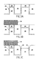
- Figure 3A illustrates a cross-section of a partially formed semiconductor transistor which includes a silicon region 300 which will become a P-well of an NFET and a silicon region 301 which will become an N- well of a PFET.
- Figure 3A also illustrates shallow trench isolation (STI) regions 302 as well as nitride pads 303, 304 which exist above the NFET silicon region 300 and the PFET silicon region 301.
- Figure 3A illustrates a nitride liner 305.
- the structure illustrated in Figure 3A is formed using well-known deposition and patterning methods.
- the flowchart in Figure 5A illustrates this portion of the invention in block 501.
- the structure is planarized using conventional methods, such as chemical-mechanical polishing, to smooth the structure down to the top of the pad nitride 303, 304.
- a layer of photoresist (or other similar masking material such as an oxide hard-masking layer) is deposited and patterned to form the WN mask (N-well mask) 310. This leaves the PFET areas 304, 301 exposed and the NFET 303, 300 areas protected by the photoresist 310.
- Figure 5A illustrates this portion of the invention in block 502.
- the exposed pad nitride layer 304 is removed using a common removal agent, such as a reactive ion etch for Si3N4 or hot H3PO4, as shown in Figure 3C.
- a common removal agent such as a reactive ion etch for Si3N4 or hot H3PO4, as shown in Figure 3C.
- the etch depth into the nitride liner 305 is determined by the length of time of the hot phosphoric etch.
- the H3PO4 etches at a rate equal to 4.5nm/min, for a planar nitride surface. This information along with experimental tuning of the etch conditions is used to determine the etch time required to recess the nitride liner to its desired depth.
- nitride etch is followed by an oxide etch (such as buffered HF), which removes the thin (i.e. 6nm) pad oxide which is commonly under the nitride pad 304. In most cases the nitride etch will also completely remove the thin pad oxide, due to the controlled overetch time. This etching produces pronounced divots 320 in the STI 302 which can easily be filled with gate conductor polysilicon (GC poly).
- Figure 5A illustrates this portion of the invention in block 503.
- the depth of the divot should be greater than the depth of the channel depletion layer to obtain good PFET performance.
- the depth of the divot in an NFET should be minimized, for the reasons discussed above.
- the divot depth for the NFET is preferably zero (no divot).
- the divot depth for the NFET is less than one-third of the depth of the depleted region of the P-well such that the gate conductor does not significantly wrap-around the silicon edge of the P-well.
- the channel depletion layer depth of a PFET is determined by the impurity (e.g., boron) implanting process.
- the depletion layer commonly has a depth of approximately 60 nm (600 angstroms) and, in such a situation, the divot depth should be approximately 100 nm (1000 angstroms) to insure good PFET performance.
- FIG. 3D The deep divot masking photoresist 310 is then removed, as shown in Figure 3D.
- Figure 5A illustrates this portion of the invention in block 504.
- the.pad nitride 303 over the remaining areas 300 is removed (again, for example, using hot H3PO4). This also removes the pad oxide underlying the pad nitride 303. Since normally practiced pad etch conditions are used, the recess of the nitride liner 305 in the non-PFET (i.e. NFET) areas 300 is kept to a minimum.
- Figure 5A illustrates this portion of the invention in block 505.
- the invention selectively controls the divot depth for different types of transistors which are formed on the same substrate (e.g., wafer) in a single manufacturing process.
- the invention is particularly useful for technologies using both buried- channel and surface-channel MOSFETs.
- buried-channel PMOSFETs and surface-channel NMOSFETs are used as an example.
- buried-channel and surface-channel MOSFETs have competing needs for divot depth.
- the foregoing embodiment of the invention adds an additional mask formation and removal step to the conventional process of manufacturing NMOSFETs and PMOSFETs.
- the second embodiment of the invention discussed below, selectively controls the divot depth for different transistor devices without requiring additional mask formation or removal steps.
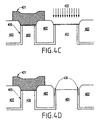
- Figure 4A is similar to Figure 3A and illustrates a silicon region to be used for an NFET 400, a silicon region to be used for a PFET 401, shallow trench isolation regions 402, a nitride liner 405 and a sacrificial oxide layer 406 grown on the exposed silicon surfaces 400, 401.
- Figure 5B illustrates this portion of the invention in block 510.
- a layer of photoresist is deposited and patterned to form the WP mask (P-well mask) 412. This leaves the NFET areas 400, 406 exposed and the PFET areas 401, 406 protected by the photoresist 412.
- a P-type impurity (such as boron) is implanted using methods well known to those ordinarily skilled in the art to establish the doping in the P-wells 400 of the NFETs.
- the flowchart in Figure 5B illustrates this portion of the invention in block 511.
- the P-well (WP) 412 photoresist is removed and another layer of photoresist is deposited and patterned as the WN (N-well) mask 421.
- This pattern protects the P-wells (NFETs) 400 from subsequent processing on the PFETs 401.
- the N-wells 401 are implanted with N-type dopants (such as phosphorus and arsenic) and a P-type dopant for the buried surface layer, again, using methods well known to those ordinarily skilled in the art.
- Figure 5B illustrates this portion of the invention in block 512.
- an oxide etch such as buffered HF
- a nitride etch (again, such as hot H3PO4) is used to recess the exposed nitride liner 405 to the desired depth 430.
- the etch depth into the nitride liner 405 is determined by the length of time of the hot phosphoric etch.
- Figure 5B illustrates this portion of the invention in block 513.
- an oxide etch is used to expand the seam 430 in the PFET areas, while the NFETS remain protected by photoresist 421. This facilitates subsequent filling of the deep divot 430 with, for example, gate conductor polysilicon (GC poly).
- GC poly gate conductor polysilicon
- Figure 5B illustrates this portion of the invention in block 514.
- the invention controls the amount of gate wrap-around within MOSFETs by adjusting the depth of divots within the shallow trench isolation regions adjacent the gates.
- the invention includes a single process which forms a deep divot in buried-channel PFET devices and a shallow divot depth in the surface-channel NFET devices on the same substrate. By doing so, the invention provides reduced sub-threshold swing, off-current, parasitic edge conduction, hot-electron degradation and sensitivity to the presence of charge adjacent to the device sidewall.
- the invention relates to technologies using both buried-channel and surface-channel MOSFETs.
- buried-channel PFET off-current and subthreshold swing are reduced, which results in lower standby power.
- the increased gate wrap-around results in increased effective channel width, higher on-current and improved performance.
Landscapes
- Metal-Oxide And Bipolar Metal-Oxide Semiconductor Integrated Circuits (AREA)
- Element Separation (AREA)
- Insulated Gate Type Field-Effect Transistor (AREA)
Abstract
Description
- The present invention generally relates to controlling the amount of gate wrap-around within metal oxide semiconductor field effect transistors by adjusting the depth of divots within the shallow trench isolation regions adjacent the gates.
- It is well recognized that divots in shallow trench isolation (STI) regions adjacent transistor wells, which are a consequence of removing the sacrificial oxide layers in surface-channel N-type metal oxide semiconductor field effect transistors (NFETs), are responsible for causing the gate conductor to "wrap- around" the silicon corners in NFETs which results in poor threshold voltage (Vt) controllability of the NFETs.
Such divots - However, a problem exists with this conventional solution of increasing the doping concentration because a drastically increased array junction leakage has been observed with increased P-well surface concentration (e.g., a surface concentration greater than 5X1017 cm-3). Because of this array NFET problem arising from the STI divot, there has been great interest in minimizing divot depth.
- The invention minimizes divot depth for NFET devices and at the same time avoids causing problems with other devices manufactured on the same wafer, such as buried-channel PFET devices.
- US Patent 5 674 775 describes a process to form isolation regions in semiconductor devices and in particular to form shallow trenches for isolation regions in semiconductor devices. The trench has rounded top edges to allow the formation of a gate oxide with uniform thickness around the trench thereby reducing parasitic field FET problems. The rounded top edges are formed by etching a substrate surface through spacers which have to be etched away before the edges are reached by the etching process.
- The article in Extended Abstracts of the 1996 International Conference on Solid State Devices and Materials, Yokohama, 1996, pp.260-262 reference XP 000694042 proposes an elevated field oxide structure referred to as Elevated Trench Isolation. The formation of trench isolation after gate oxidation allows the use of BPSG as trench filling material and is claimed to provide void-free gap filling in an aspect ratio of 3.5. The transistors have a wrap around gate.
- The Patent Abstracts of Japan, Vol. 1999, No. 1, AB Date 29.01.1999 & JP10 290 009A describes a first transistor located between shallow trench isolation regions having a wrap around gate and a second transistor also having a wrap around gate.
- A semiconductor structure according to the present invention is defined in claim 1.
- In a further aspect, the invention provides a method of manufacturing the semiconductor structure as described in the preceding paragraph comprising the steps of: forming the plurality of transistor P-wells and N-wells separated by the isolation regions; protecting the N-wells with a first patterned mask and leaving the P-wells exposed; implanting a first impurity in said P-wells; removing said first patterned mask; protecting said P-wells with a second patterned mask and leaving said N-wells exposed; implanting a second and third impurity in said N-wells; forming the first divots in areas of said isolation regions adjacent said N-wells; removing said second patterned mask; and forming the second divots in areas of said isolation regions adjacent said P-wells.
- Preferably a semiconductor substrate is provided and first gate conductors which wrap around N-wells of buried channel P-type metal oxide semiconductor field effect transistors and second gate conductors which do not wrap around P-wells of buried channel N-type metal oxide semiconductor field effect transistors.
- Preferably a method is provided which comprises forming insulators adjacent each of the N-wells and the P-wells, protecting the P-wells with a patterned mask, forming first divots in areas of the insulators adjacent the N-wells and forming second divots in areas of the insulators adjacent P-wells, wherein the first divots have a greater depth than the second divots.
- In a preferred embodiment, the process of forming the first N-divots comprises etching the insulators from portions of sides of the wells and the process of forming the second divots maintains the insulators on sides of the P-wells.
- The method also preferably includes forming gate conductors over the N-wells and the P-wells, such that respective ones of the gate conductors cover a top surface of the P-wells and others of the gate conductors cover a top surface and side surfaces of the N-wells. Additionally, the N-wells preferably have a depleted region within a surface P-layer and the first divots are formed to have a depth greater than a depth of the depleted region.
- In another embodiment the method includes forming insulators adjacent each of the N-wells and the P-wells, protecting the N-wells with a patterned mask and leaving the P-wells exposed, implanting a first impurity in the P-wells, removing the first patterned mask, protecting the P-wells with a second patterned mask and leaving the N-wells exposed, implanting a second and third impurity in the N-wells, forming first divots in areas of the insulators adjacent the N-wells, removing the second patterned mask, and forming second divots in areas of the insulators adjacent the P-wells, wherein the first divots have a greater depth than the second divots.
- In one embodiment, the invention also comprises a semiconductor structure having buried-channel P-type metal oxide semiconductor field effect transistors having N-wells and first gate conductors covering tops and portions of sides of the N-wells, and surface-channel N-type metal oxide semiconductor field effect transistors having P-wells and second gate conductors covering tops of the P-wells.
- In one embodiment, the inventive structure also includes first shallow trench isolation (STI) regions adjacent the N-wells and having first divots, and second shallow trench isolation regions (STI) adjacent the P-wells and having second divots, wherein the first divots have a depth greater than that of the second divots. Also, the N-wells include a depleted P-type region adjacent the first gate conductors and the first gate conductors cover the sides of the N-wells to a depth greater than a depth of the depleted P-type region. Further, in one embodiment the N-wells and the P-wells are positioned on a single substrate.
- The invention controls the amount of gate wrap-around within field effect transistors by adjusting the depth of divots within the shallow trench isolation regions adjacent the gates. The invention is a single process which forms a deep divot in buried-channel PFET devices and a shallow divot depth in surface-channel NFET devices on the same substrate and, by doing so, provides reduced sub-threshold swing, off-current, parasitic edge conduction, hot-electron degradation and sensitivity to the presence of charge adjacent to the device sidewall.
- The foregoing and other objects, aspects and advantages will be better understood from the following detailed description of preferred embodiments of the invention with reference to the drawings, in which:
- Figure 1 is a schematic diagram of a cross-sectional view of a P-type buried-channel field effect transistor;
- Figure 2 is a graph showing the relationship between current and voltage for the different sides of the structure shown in Figure 1;
- Figures 3A-3D are schematic diagrams of cross-sectional views of field effect transistors which demonstrate an embodiment of the invention;
- Figures 4A-4D are schematic diagrams of cross-sectional views of field effect transistors which demonstrate an embodiment of the invention; and
- Figure 5A-5B are flowcharts illustrating preferred embodiments of the invention.
-
- As mentioned above, divots in shallow trench isolation (STI) regions adjacent transistor well regions, which are a consequence of removing the sacrificial oxide layers in metal oxide semiconductor field effect transistors are responsible for causing the gate conductor to wrap-around the silicon edge which results in poor threshold voltage (Vt) controllability of array NFETs. Therefore, there has been great interest in minimizing the divot depth. Ideally, it is desired that the divots adjacent transistor well regions in surface-channel N-type NFETs have zero depth.
- The present inventors have discovered that a shallow STI divot depth, which is necessary for controlling corner conduction in surface-channel NFETs, is detrimental to the operation of the buried-channel P-type metal oxide semiconductor field effect transistors (referred to herein as PMOSFETs or PFETs). Shallow STI divot depth results in poor Ioff gate control at the edge of the buried-channel PFET, making the PFET device susceptible to sidewall parasitic conduction, poor subthreshold slope and hot-electron degradation.
- Figure 1 is a schematic drawing of a cross-section of a buried-channel PFET device having a
deep divot 13 on its left side and ashallow divot 12 on its right side. Additionally, Figure 1 illustrates agate conductor 14 which, in this example, is an N+ polysilicon gate conductor, and a depleted P-layer 15 above an N-well 11 which is surrounded by anitride layer 16. Agate oxide layer 18 separates thegate conductor 14 from thedepleted region 15. Thenitride layer 16 is bordered by shallow trench isolation (STI)regions 10. - Contrary to the effect on surface-channel NFETs, the
shallow divot 12 results in parasitic edge conduction in the buried-channel PFET. Loss of gate control degrades sub-threshold slope, off-current and hot-electron reliability. - In order to assure acceptable off-current for the buried-channel PFET, the
gate 14 must have strong enough control of the electric potential throughout the surface P-layer 15 such that the P-layer 15 is strongly depleted of majority carriers (holes). Gate wrap-around actually increases the control of the electric potential throughout the surface of the P-layer. - In the presence of the
deep STI divot 13, the gate wrap-around of the corner allows the sidewall of the P-layer 15 to be fully depleted of holes. However with theshallow divot 12, the sidewall is weakly controlled by thegate 14. This results in high off-current and degraded sub-threshold slope. - Figure 2 illustrates the voltage/current slope (e.g, the majority carrier depletion at the sidewalls) for the
shallow divot 12 inline 22 and the voltage/current slope for thedeep divot 13 inline 21. As shown in Figure 2, the slope ofline 22 produced by theshallow divot 12 is severely degraded from the more preferable slope ofline 21 produced by thedeep divot 13. Further, thedeep divot 13 has a much lower off-current 20 than the undesirable elevated off-current 23 associated with theshallow divot 12. - The
deep divot 13 has a depth that extends below the depth of the P- layer/N-well junction. which allows the P-layer at the left hand side of the device to become completely depleted, making no contribution to off-current (ideally). The P-layer at the sidewall of right hand side of the device contains anundepleted region 17, since the gate is unable to control the potential in that part of the device. Thus, theright hand sidewall 17 contributes significantly to the elevated off-current. - Furthermore, since the top part of the
nitride liner 16 is adjacent the sidewall P-layer 17 on the right hand side, any electrons which are trapped near the P-layer/nitride interface induce sidewall leakage. Trapped electrons may be process induced or may result from hot-electron degradation of the device during normal operation. - On the other hand, the
nitride liner 16 on the left sidewall of the device is substantially recessed below the depth of the P-layer/N-well junction. This deep recess of thenitride liner 16 results in a significant reduction in trapped electron density in the region which is susceptible to parasitic conduction. The substantial absence of thenitride liner 16 significantly reduces the rate of hot-e degradation. - Preferred methods of the invention, which are described below, allow a deep divot to be fabricated on the PFETs and a shallow divot on the NFETs. The STI divot depth of the PFET may be tailored independently of the divot depth of the NFET. Thus, the invention controls the amount of gate wrap-around within MOSFETs by adjusting the depth of divots within the shallow trench isolation regions adjacent the gates.
- More specifically, Figure 3A illustrates a cross-section of a partially formed semiconductor transistor which includes a
silicon region 300 which will become a P-well of an NFET and asilicon region 301 which will become an N- well of a PFET. Figure 3A also illustrates shallow trench isolation (STI)regions 302 as well asnitride pads NFET silicon region 300 and thePFET silicon region 301. In addition Figure 3A illustrates anitride liner 305. - The structure illustrated in Figure 3A is formed using well-known deposition and patterning methods. The flowchart in Figure 5A illustrates this portion of the invention in
block 501. The structure is planarized using conventional methods, such as chemical-mechanical polishing, to smooth the structure down to the top of thepad nitride - As shown in Figure 3B, a layer of photoresist (or other similar masking material such as an oxide hard-masking layer) is deposited and patterned to form the WN mask (N-well mask) 310. This leaves the
PFET areas NFET photoresist 310. Figure 5A illustrates this portion of the invention inblock 502. - The exposed
pad nitride layer 304 is removed using a common removal agent, such as a reactive ion etch for Si3N4 or hot H3PO4, as shown in Figure 3C. The etch depth into thenitride liner 305 is determined by the length of time of the hot phosphoric etch. Typically, the H3PO4 etches at a rate equal to 4.5nm/min, for a planar nitride surface. This information along with experimental tuning of the etch conditions is used to determine the etch time required to recess the nitride liner to its desired depth. - The nitride etch is followed by an oxide etch (such as buffered HF), which removes the thin (i.e. 6nm) pad oxide which is commonly under the
nitride pad 304. In most cases the nitride etch will also completely remove the thin pad oxide, due to the controlled overetch time. This etching produces pronounceddivots 320 in theSTI 302 which can easily be filled with gate conductor polysilicon (GC poly). Figure 5A illustrates this portion of the invention inblock 503. - The depth of the divot should be greater than the depth of the channel depletion layer to obtain good PFET performance. On the other hand, the depth of the divot in an NFET should be minimized, for the reasons discussed above. The divot depth for the NFET is preferably zero (no divot). However, more realistically, the divot depth for the NFET is less than one-third of the depth of the depleted region of the P-well such that the gate conductor does not significantly wrap-around the silicon edge of the P-well.
- The channel depletion layer depth of a PFET is determined by the impurity (e.g., boron) implanting process. For example, the depletion layer commonly has a depth of approximately 60 nm (600 angstroms) and, in such a situation, the divot depth should be approximately 100 nm (1000 angstroms) to insure good PFET performance.
- The deep
divot masking photoresist 310 is then removed, as shown in Figure 3D. Figure 5A illustrates this portion of the invention inblock 504. Then,the.pad nitride 303 over the remainingareas 300 is removed (again, for example, using hot H3PO4). This also removes the pad oxide underlying thepad nitride 303. Since normally practiced pad etch conditions are used, the recess of thenitride liner 305 in the non-PFET (i.e. NFET)areas 300 is kept to a minimum. - well known processes are used to complete the formation of the semiconductor transistors including sacrificial oxidation layer formation, well implant formation, gate oxidation layer formation, gate conductor deposition and patterning, and other steps well known to those ordinarily skilled in the art. Figure 5A illustrates this portion of the invention in
block 505. - Therefore, the invention selectively controls the divot depth for different types of transistors which are formed on the same substrate (e.g., wafer) in a single manufacturing process.
- The invention is particularly useful for technologies using both buried- channel and surface-channel MOSFETs. In this application, buried-channel PMOSFETs and surface-channel NMOSFETs are used as an example. As discussed herein, buried-channel and surface-channel MOSFETs have competing needs for divot depth.
- The foregoing embodiment of the invention adds an additional mask formation and removal step to the conventional process of manufacturing NMOSFETs and PMOSFETs. The second embodiment of the invention, discussed below, selectively controls the divot depth for different transistor devices without requiring additional mask formation or removal steps.
- The second preferred method for accomplishing the invention is illustrated in Figures 4A-4D and Figure 5B. Figure 4A is similar to Figure 3A and illustrates a silicon region to be used for an
NFET 400, a silicon region to be used for aPFET 401, shallowtrench isolation regions 402, anitride liner 405 and asacrificial oxide layer 406 grown on the exposedsilicon surfaces block 510. - As shown in Figure 4B, a layer of photoresist is deposited and patterned to form the WP mask (P-well mask) 412. This leaves the
NFET areas PFET areas photoresist 412. A P-type impurity (such as boron) is implanted using methods well known to those ordinarily skilled in the art to establish the doping in the P-wells 400 of the NFETs. The flowchart in Figure 5B illustrates this portion of the invention inblock 511. - Referring to Figure 4C, the P-well (WP) 412 photoresist is removed and another layer of photoresist is deposited and patterned as the WN (N-well)
mask 421. This pattern protects the P-wells (NFETs) 400 from subsequent processing on thePFETs 401. The N-wells 401 are implanted with N-type dopants (such as phosphorus and arsenic) and a P-type dopant for the buried surface layer, again, using methods well known to those ordinarily skilled in the art. Figure 5B illustrates this portion of the invention inblock 512. - However, as shown in Figure 4D, before the removal of the
WN photoresist 421, an oxide etch (such as buffered HF) is performed to remove any sacrificial oxide covering the ends of thenitride liner 405 in thePFET areas 401. Then a nitride etch (again, such as hot H3PO4) is used to recess the exposednitride liner 405 to the desireddepth 430. As in the first embodiment, the etch depth into thenitride liner 405 is determined by the length of time of the hot phosphoric etch. Figure 5B illustrates this portion of the invention inblock 513. - Once a seam has been opened by the removal of the
nitride liner 405, an oxide etch is used to expand theseam 430 in the PFET areas, while the NFETS remain protected byphotoresist 421. This facilitates subsequent filling of thedeep divot 430 with, for example, gate conductor polysilicon (GC poly). The N-well photoresist 421 is then removed, followed by the removal of thesacrificial oxide layer 406. - As with the previous embodiment, well known processes are used to complete the formation of the semiconductor transistors including gate oxide layer formation, gate conductor deposition and patterning, and other steps well known to those ordinarily skilled in the art. Figure 5B illustrates this portion of the invention in
block 514. - A low cost process modification for increasing the divot depth of the STI adjacent to the buried-channel PFETs, without affecting the NFETs, has been described. The invention controls the amount of gate wrap-around within MOSFETs by adjusting the depth of divots within the shallow trench isolation regions adjacent the gates. The invention includes a single process which forms a deep divot in buried-channel PFET devices and a shallow divot depth in the surface-channel NFET devices on the same substrate. By doing so, the invention provides reduced sub-threshold swing, off-current, parasitic edge conduction, hot-electron degradation and sensitivity to the presence of charge adjacent to the device sidewall.
- As discussed above, the invention relates to technologies using both buried-channel and surface-channel MOSFETs. For the buried-channel PFET, off-current and subthreshold swing are reduced, which results in lower standby power. Further, the increased gate wrap-around results in increased effective channel width, higher on-current and improved performance.
- For the surface-channel NFET, divot depth is reduced. There is better Vt control and improved performance since nominal Vt may be set lower without exceeding a worst case off-current target.
Claims (9)
- A semiconductor structure comprising:wherein said first divots have a depth greater than that of said second divots.a plurality of buried-channel P-type metal oxide semiconductor field effect transistors (PFET) having N-wells (301, 401) and first gate conductors covering tops and portions of sides of said N-wells;a plurality of surface-channel N-type metal oxide field effect transistors (NFET) having P-wells (300, 400) and second gate conductors covering tops of said P-wells;first shallow trench isolation (STI) regions (302, 402) adjacent said N-wells and having first divots; andsecond shallow trench isolation regions (STI) adjacent said P-wells and having second divots ;
- The semiconductor structure of claim 1, wherein said N-wells (301, 401) include a depleted P-type region adjacent said first gate conductors and said first gate conductors cover said sides of said N-wells to a depth greater than the depth of said depleted P-type region.
- The semiconductor structure of claim 1 or 2, wherein the said N-wells and P-wells are positioned on a single substrate.
- A method of manufacturing the semiconductor structure of claim 1, 2 or 3 comprising the steps of:forming the plurality of transistor P-wells (400) and N-wells (401) separated by the isolation regions (STI);protecting the N-wells (401) with a first patterned mask (412) and leaving the P-wells (400) exposed;implanting a first impurity (411) in said P-wells (400);removing said first patterned mask (412);protecting said P-wells (400) with a second patterned mask (421) and leaving said N-wells (401) exposed;implanting a second and third impurity (422) in said N-wells (401);forming the first divots (430) in areas of said isolation regions (STI) adjacent said N-wells (401);removing said second patterned mask (421); andforming the second divots in areas of said isolation regions (STI) adjacent said P-wells (400).
- A method of manufacturing the semiconductor structure of claim 1, 2 or 3, comprising the steps of:forming the plurality of transistor P-wells (300) and N-wells (301) separated by the isolation regions (302);protecting said P-wells with a patterned mask (310) and leaving said N-wells (301) exposed;forming the first divots (320) in areas of the isolation regions (302) adjacent to the N-wells (301);removing said patterned mask (310); andcompleting the formation of the semiconductor transistors.
- The method of claim 4 or 5, wherein the wells are silicon wells surrounded by nitride and separated by the shallow trench insulation regions (STI).
- The method of claim 4, 5 or 6, wherein said first divots are formed by etching said isolation regions from portions of sides of said N-wells and said second divots maintain said isolation regions on sides of said P-wells.
- The method of claim 4, 5, 6 or 7 further comprising forming gate conductors over said transistor wells, such that respective ones of said gate conductors cover a top surface of said P-wells and others of said gate conductors cover a top surface and side surfaces of said N-wells.
- The method of any one of claims 4 to 8, wherein said wells have a depleted region and said first divots are formed to have a depth greater than the depth of said depleted region.
Applications Claiming Priority (2)
| Application Number | Priority Date | Filing Date | Title |
|---|---|---|---|
| US09/181,964 US6127215A (en) | 1998-10-29 | 1998-10-29 | Deep pivot mask for enhanced buried-channel PFET performance and reliability |
| US181964 | 1998-10-29 |
Publications (2)
| Publication Number | Publication Date |
|---|---|
| EP0997946A1 EP0997946A1 (en) | 2000-05-03 |
| EP0997946B1 true EP0997946B1 (en) | 2003-01-02 |
Family
ID=22666548
Family Applications (1)
| Application Number | Title | Priority Date | Filing Date |
|---|---|---|---|
| EP99308122A Expired - Lifetime EP0997946B1 (en) | 1998-10-29 | 1999-10-14 | Deep divot in shallow trench isolation for a buried-channel PFET |
Country Status (7)
| Country | Link |
|---|---|
| US (2) | US6127215A (en) |
| EP (1) | EP0997946B1 (en) |
| JP (1) | JP3364903B2 (en) |
| KR (1) | KR100375032B1 (en) |
| AT (1) | ATE230520T1 (en) |
| DE (1) | DE69904690T2 (en) |
| TW (1) | TW426943B (en) |
Families Citing this family (23)
| Publication number | Priority date | Publication date | Assignee | Title |
|---|---|---|---|---|
| JP2002033476A (en) * | 2000-07-13 | 2002-01-31 | Mitsubishi Electric Corp | Semiconductor device and method of manufacturing the same |
| DE10131710B4 (en) * | 2001-06-29 | 2006-05-18 | Infineon Technologies Ag | Method for the targeted adjustment of the step height in STI technology for the production of integrated circuits |
| US6759298B2 (en) * | 2002-06-24 | 2004-07-06 | Micron Technology, Inc. | Methods of forming an array of flash field effect transistors and circuitry peripheral to such array |
| US6605504B1 (en) | 2002-06-28 | 2003-08-12 | Infineon Technologies Ag | Method of manufacturing circuit with buried strap including a liner |
| US20040040105A1 (en) * | 2002-09-03 | 2004-03-04 | Hillenbrand Stephen John | Scuff remover device |
| US6743675B2 (en) | 2002-10-01 | 2004-06-01 | Mosel Vitelic, Inc. | Floating gate memory fabrication methods comprising a field dielectric etch with a horizontal etch component |
| US20040065937A1 (en) * | 2002-10-07 | 2004-04-08 | Chia-Shun Hsiao | Floating gate memory structures and fabrication methods |
| DE10329212B4 (en) * | 2003-06-28 | 2006-07-06 | Infineon Technologies Ag | Method for producing an integrated DRAM memory circuit with corner devices |
| US6838342B1 (en) * | 2003-10-03 | 2005-01-04 | Promos Technologies, Inc. | Nonvolatile memory fabrication methods comprising lateral recessing of dielectric sidewalls at substrate isolation regions |
| US7091091B2 (en) * | 2004-06-28 | 2006-08-15 | Promos Technologies Inc. | Nonvolatile memory fabrication methods in which a dielectric layer underlying a floating gate layer is spaced from an edge of an isolation trench and/or an edge of the floating gate layer |
| US7132333B2 (en) * | 2004-09-10 | 2006-11-07 | Infineon Technologies Ag | Transistor, memory cell array and method of manufacturing a transistor |
| KR100618892B1 (en) * | 2005-04-13 | 2006-09-01 | 삼성전자주식회사 | Semiconductor package achieves fan-out structure through wire bonding |
| DE102005037566B4 (en) * | 2005-08-09 | 2008-04-24 | Qimonda Ag | Manufacturing method for a semiconductor structure and corresponding semiconductor structure |
| US20080099834A1 (en) * | 2006-10-30 | 2008-05-01 | Josef Willer | Transistor, an inverter and a method of manufacturing the same |
| US8642441B1 (en) | 2006-12-15 | 2014-02-04 | Spansion Llc | Self-aligned STI with single poly for manufacturing a flash memory device |
| US20080258206A1 (en) * | 2007-04-17 | 2008-10-23 | Qimonda Ag | Self-Aligned Gate Structure, Memory Cell Array, and Methods of Making the Same |
| US20080283910A1 (en) * | 2007-05-15 | 2008-11-20 | Qimonda Ag | Integrated circuit and method of forming an integrated circuit |
| US7838355B2 (en) * | 2008-06-04 | 2010-11-23 | International Business Machines Corporation | Differential nitride pullback to create differential NFET to PFET divots for improved performance versus leakage |
| US8551858B2 (en) * | 2010-02-03 | 2013-10-08 | Spansion Llc | Self-aligned SI rich nitride charge trap layer isolation for charge trap flash memory |
| US8461634B2 (en) | 2011-04-14 | 2013-06-11 | Taiwan Semiconductor Manufacturing Company, Ltd. | Divot engineering for enhanced device performance |
| US10796943B2 (en) * | 2018-11-06 | 2020-10-06 | United Microelectronics Corp. | Manufacturing method of semiconductor structure |
| CN115915749B (en) * | 2023-01-19 | 2023-06-02 | 合肥晶合集成电路股份有限公司 | Semiconductor structure and manufacturing method thereof |
| USD1117470S1 (en) * | 2024-06-26 | 2026-03-10 | Sky Fabrication Inc. | Gripping tool |
Family Cites Families (19)
| Publication number | Priority date | Publication date | Assignee | Title |
|---|---|---|---|---|
| US3136897A (en) * | 1961-09-25 | 1964-06-09 | Westinghouse Electric Corp | Monolithic semiconductor structure comprising at least one junction transistor and associated diodes to form logic element |
| JPS5935445A (en) * | 1982-08-24 | 1984-02-27 | Nippon Telegr & Teleph Corp <Ntt> | Manufacture of semiconductor device |
| US4663832A (en) * | 1984-06-29 | 1987-05-12 | International Business Machines Corporation | Method for improving the planarity and passivation in a semiconductor isolation trench arrangement |
| IT1200725B (en) * | 1985-08-28 | 1989-01-27 | Sgs Microelettronica Spa | INSULATION STRUCTURE IN MOS DEVICES AND ITS PREPARATION PROCEDURE |
| US4842675A (en) * | 1986-07-07 | 1989-06-27 | Texas Instruments Incorporated | Integrated circuit isolation process |
| US4863562A (en) * | 1988-02-11 | 1989-09-05 | Sgs-Thomson Microelectronics, Inc. | Method for forming a non-planar structure on the surface of a semiconductor substrate |
| US4900692A (en) * | 1989-04-24 | 1990-02-13 | Motorola, Inc. | Method of forming an oxide liner and active area mask for selective epitaxial growth in an isolation trench |
| EP0603106A2 (en) * | 1992-12-16 | 1994-06-22 | International Business Machines Corporation | Method to reduce stress from trench structure on SOI wafer |
| US5387540A (en) * | 1993-09-30 | 1995-02-07 | Motorola Inc. | Method of forming trench isolation structure in an integrated circuit |
| KR950021600A (en) * | 1993-12-09 | 1995-07-26 | 가나이 쯔또무 | Semiconductor integrated circuit device and manufacturing method thereof |
| JP2955459B2 (en) * | 1993-12-20 | 1999-10-04 | 株式会社東芝 | Method for manufacturing semiconductor device |
| US5447884A (en) * | 1994-06-29 | 1995-09-05 | International Business Machines Corporation | Shallow trench isolation with thin nitride liner |
| US5652176A (en) * | 1995-02-24 | 1997-07-29 | Motorola, Inc. | Method for providing trench isolation and borderless contact |
| JPH09312429A (en) * | 1996-05-21 | 1997-12-02 | Sony Corp | Anti-vibration device in laser equipment and optical disc master manufacturing device using the device |
| US5858866A (en) * | 1996-11-22 | 1999-01-12 | International Business Machines Corportation | Geometrical control of device corner threshold |
| US5674775A (en) * | 1997-02-20 | 1997-10-07 | Taiwan Semiconductor Manufacturing Company, Ltd. | Isolation trench with a rounded top edge using an etch buffer layer |
| US6153478A (en) * | 1998-01-28 | 2000-11-28 | United Microelectronics Corp. | STI process for eliminating kink effect |
| TW444333B (en) * | 1998-07-02 | 2001-07-01 | United Microelectronics Corp | Method for forming corner rounding of shallow trench isolation |
| KR100281124B1 (en) * | 1999-01-20 | 2001-01-15 | 김영환 | Semicon ductor and method for fabricating the same |
-
1998
- 1998-10-29 US US09/181,964 patent/US6127215A/en not_active Expired - Fee Related
-
1999
- 1999-10-04 TW TW088117065A patent/TW426943B/en not_active IP Right Cessation
- 1999-10-13 JP JP29109099A patent/JP3364903B2/en not_active Expired - Fee Related
- 1999-10-14 EP EP99308122A patent/EP0997946B1/en not_active Expired - Lifetime
- 1999-10-14 AT AT99308122T patent/ATE230520T1/en not_active IP Right Cessation
- 1999-10-14 DE DE69904690T patent/DE69904690T2/en not_active Expired - Lifetime
- 1999-10-28 KR KR10-1999-0047025A patent/KR100375032B1/en not_active Expired - Fee Related
-
2000
- 2000-07-03 US US09/609,379 patent/US6323532B1/en not_active Expired - Fee Related
Also Published As
| Publication number | Publication date |
|---|---|
| US6323532B1 (en) | 2001-11-27 |
| DE69904690T2 (en) | 2003-09-18 |
| KR100375032B1 (en) | 2003-03-08 |
| JP2000269441A (en) | 2000-09-29 |
| US6127215A (en) | 2000-10-03 |
| JP3364903B2 (en) | 2003-01-08 |
| EP0997946A1 (en) | 2000-05-03 |
| DE69904690D1 (en) | 2003-02-06 |
| ATE230520T1 (en) | 2003-01-15 |
| TW426943B (en) | 2001-03-21 |
| KR20000029367A (en) | 2000-05-25 |
Similar Documents
| Publication | Publication Date | Title |
|---|---|---|
| US6127215A (en) | Deep pivot mask for enhanced buried-channel PFET performance and reliability | |
| KR100259097B1 (en) | Semiconductor device and method for fabricating the same | |
| US7288470B2 (en) | Semiconductor device comprising buried channel region and method for manufacturing the same | |
| KR100243715B1 (en) | CMOS structure with FET in isolated well with depletion unit and method | |
| US6255152B1 (en) | Method of fabricating CMOS using Si-B layer to form source/drain extension junction | |
| US6599789B1 (en) | Method of forming a field effect transistor | |
| KR0165457B1 (en) | Trench element isolation | |
| US5994179A (en) | Method of fabricating a MOSFET featuring an effective suppression of reverse short-channel effect | |
| EP1125326B1 (en) | Selectively doped trench device isolation | |
| KR100680958B1 (en) | Manufacturing method of PMOS transistor | |
| US6649460B2 (en) | Fabricating a substantially self-aligned MOSFET | |
| US6703187B2 (en) | Method of forming a self-aligned twin well structure with a single mask | |
| US6350638B2 (en) | Method of forming complementary type conductive regions on a substrate | |
| KR100597462B1 (en) | Method for fabricating transistor of semiconductor device | |
| JP2000150870A (en) | Semiconductor device and manufacturing method thereof | |
| KR100609532B1 (en) | Manufacturing Method of SOI Semiconductor Device | |
| KR20040058832A (en) | Soi semiconductor device and method for manufacturing the same | |
| HK1035260A1 (en) | Deep divot mask for enhanced buried-channel pfet performance and reliability | |
| HK1035260B (en) | Deep divot mask for enhanced buried-channel pfet performance and reliability |
Legal Events
| Date | Code | Title | Description |
|---|---|---|---|
| PUAI | Public reference made under article 153(3) epc to a published international application that has entered the european phase |
Free format text: ORIGINAL CODE: 0009012 |
|
| AK | Designated contracting states |
Kind code of ref document: A1 Designated state(s): AT BE CH CY DE DK ES FI FR GB GR IE IT LI LU MC NL PT SE |
|
| AX | Request for extension of the european patent |
Free format text: AL;LT;LV;MK;RO;SI |
|
| 17P | Request for examination filed |
Effective date: 20001016 |
|
| AKX | Designation fees paid |
Free format text: AT BE CH CY DE DK ES FI FR GB GR IE IT LI LU MC NL PT SE |
|
| 17Q | First examination report despatched |
Effective date: 20010726 |
|
| GRAG | Despatch of communication of intention to grant |
Free format text: ORIGINAL CODE: EPIDOS AGRA |
|
| GRAG | Despatch of communication of intention to grant |
Free format text: ORIGINAL CODE: EPIDOS AGRA |
|
| GRAG | Despatch of communication of intention to grant |
Free format text: ORIGINAL CODE: EPIDOS AGRA |
|
| GRAH | Despatch of communication of intention to grant a patent |
Free format text: ORIGINAL CODE: EPIDOS IGRA |
|
| GRAH | Despatch of communication of intention to grant a patent |
Free format text: ORIGINAL CODE: EPIDOS IGRA |
|
| GRAA | (expected) grant |
Free format text: ORIGINAL CODE: 0009210 |
|
| AK | Designated contracting states |
Kind code of ref document: B1 Designated state(s): AT BE CH CY DE DK ES FI FR GB GR IE IT LI LU MC NL PT SE |
|
| PG25 | Lapsed in a contracting state [announced via postgrant information from national office to epo] |
Ref country code: NL Free format text: LAPSE BECAUSE OF FAILURE TO SUBMIT A TRANSLATION OF THE DESCRIPTION OR TO PAY THE FEE WITHIN THE PRESCRIBED TIME-LIMIT Effective date: 20030102 Ref country code: LI Free format text: LAPSE BECAUSE OF FAILURE TO SUBMIT A TRANSLATION OF THE DESCRIPTION OR TO PAY THE FEE WITHIN THE PRESCRIBED TIME-LIMIT Effective date: 20030102 Ref country code: IT Free format text: LAPSE BECAUSE OF FAILURE TO SUBMIT A TRANSLATION OF THE DESCRIPTION OR TO PAY THE FEE WITHIN THE PRESCRIBED TIME-LIMIT;WARNING: LAPSES OF ITALIAN PATENTS WITH EFFECTIVE DATE BEFORE 2007 MAY HAVE OCCURRED AT ANY TIME BEFORE 2007. THE CORRECT EFFECTIVE DATE MAY BE DIFFERENT FROM THE ONE RECORDED. Effective date: 20030102 Ref country code: GR Free format text: LAPSE BECAUSE OF FAILURE TO SUBMIT A TRANSLATION OF THE DESCRIPTION OR TO PAY THE FEE WITHIN THE PRESCRIBED TIME-LIMIT Effective date: 20030102 Ref country code: FI Free format text: LAPSE BECAUSE OF FAILURE TO SUBMIT A TRANSLATION OF THE DESCRIPTION OR TO PAY THE FEE WITHIN THE PRESCRIBED TIME-LIMIT Effective date: 20030102 Ref country code: CH Free format text: LAPSE BECAUSE OF FAILURE TO SUBMIT A TRANSLATION OF THE DESCRIPTION OR TO PAY THE FEE WITHIN THE PRESCRIBED TIME-LIMIT Effective date: 20030102 Ref country code: BE Free format text: LAPSE BECAUSE OF FAILURE TO SUBMIT A TRANSLATION OF THE DESCRIPTION OR TO PAY THE FEE WITHIN THE PRESCRIBED TIME-LIMIT Effective date: 20030102 Ref country code: AT Free format text: LAPSE BECAUSE OF FAILURE TO SUBMIT A TRANSLATION OF THE DESCRIPTION OR TO PAY THE FEE WITHIN THE PRESCRIBED TIME-LIMIT Effective date: 20030102 |
|
| REF | Corresponds to: |
Ref document number: 230520 Country of ref document: AT Date of ref document: 20030115 Kind code of ref document: T |
|
| REG | Reference to a national code |
Ref country code: GB Ref legal event code: FG4D Free format text: 20030102 |
|
| REG | Reference to a national code |
Ref country code: CH Ref legal event code: EP |
|
| REG | Reference to a national code |
Ref country code: IE Ref legal event code: FG4D |
|
| REF | Corresponds to: |
Ref document number: 69904690 Country of ref document: DE Date of ref document: 20030206 Kind code of ref document: P |
|
| RAP2 | Party data changed (patent owner data changed or rights of a patent transferred) |
Owner name: INFINEON TECHNOLOGIES AG Owner name: INTERNATIONAL BUSINESS MACHINES CORPORATION |
|
| PG25 | Lapsed in a contracting state [announced via postgrant information from national office to epo] |
Ref country code: SE Free format text: LAPSE BECAUSE OF FAILURE TO SUBMIT A TRANSLATION OF THE DESCRIPTION OR TO PAY THE FEE WITHIN THE PRESCRIBED TIME-LIMIT Effective date: 20030402 Ref country code: PT Free format text: LAPSE BECAUSE OF FAILURE TO SUBMIT A TRANSLATION OF THE DESCRIPTION OR TO PAY THE FEE WITHIN THE PRESCRIBED TIME-LIMIT Effective date: 20030402 Ref country code: DK Free format text: LAPSE BECAUSE OF FAILURE TO SUBMIT A TRANSLATION OF THE DESCRIPTION OR TO PAY THE FEE WITHIN THE PRESCRIBED TIME-LIMIT Effective date: 20030402 |
|
| NLT2 | Nl: modifications (of names), taken from the european patent patent bulletin |
Owner name: INTERNATIONAL BUSINESS MACHINES CORPORATION EN INF |
|
| ET | Fr: translation filed | ||
| REG | Reference to a national code |
Ref country code: CH Ref legal event code: PL |
|
| PG25 | Lapsed in a contracting state [announced via postgrant information from national office to epo] |
Ref country code: ES Free format text: LAPSE BECAUSE OF FAILURE TO SUBMIT A TRANSLATION OF THE DESCRIPTION OR TO PAY THE FEE WITHIN THE PRESCRIBED TIME-LIMIT Effective date: 20030730 |
|
| PG25 | Lapsed in a contracting state [announced via postgrant information from national office to epo] |
Ref country code: LU Free format text: LAPSE BECAUSE OF NON-PAYMENT OF DUE FEES Effective date: 20031014 Ref country code: CY Free format text: LAPSE BECAUSE OF FAILURE TO SUBMIT A TRANSLATION OF THE DESCRIPTION OR TO PAY THE FEE WITHIN THE PRESCRIBED TIME-LIMIT Effective date: 20031014 |
|
| PG25 | Lapsed in a contracting state [announced via postgrant information from national office to epo] |
Ref country code: MC Free format text: LAPSE BECAUSE OF NON-PAYMENT OF DUE FEES Effective date: 20031031 |
|
| PLBE | No opposition filed within time limit |
Free format text: ORIGINAL CODE: 0009261 |
|
| STAA | Information on the status of an ep patent application or granted ep patent |
Free format text: STATUS: NO OPPOSITION FILED WITHIN TIME LIMIT |
|
| 26N | No opposition filed |
Effective date: 20031003 |
|
| REG | Reference to a national code |
Ref country code: IE Ref legal event code: MM4A |
|
| PGFP | Annual fee paid to national office [announced via postgrant information from national office to epo] |
Ref country code: IE Payment date: 20071023 Year of fee payment: 9 |
|
| PG25 | Lapsed in a contracting state [announced via postgrant information from national office to epo] |
Ref country code: IE Free format text: LAPSE BECAUSE OF NON-PAYMENT OF DUE FEES Effective date: 20081014 |
|
| PGFP | Annual fee paid to national office [announced via postgrant information from national office to epo] |
Ref country code: FR Payment date: 20101018 Year of fee payment: 12 |
|
| PGFP | Annual fee paid to national office [announced via postgrant information from national office to epo] |
Ref country code: GB Payment date: 20101021 Year of fee payment: 12 |
|
| GBPC | Gb: european patent ceased through non-payment of renewal fee |
Effective date: 20111014 |
|
| REG | Reference to a national code |
Ref country code: FR Ref legal event code: ST Effective date: 20120629 |
|
| PG25 | Lapsed in a contracting state [announced via postgrant information from national office to epo] |
Ref country code: FR Free format text: LAPSE BECAUSE OF NON-PAYMENT OF DUE FEES Effective date: 20111102 Ref country code: GB Free format text: LAPSE BECAUSE OF NON-PAYMENT OF DUE FEES Effective date: 20111014 |
|
| REG | Reference to a national code |
Ref country code: DE Ref legal event code: R081 Ref document number: 69904690 Country of ref document: DE Owner name: INFINEON TECHNOLOGIES AG, DE Free format text: FORMER OWNERS: INTERNATIONAL BUSINESS MACHINES CORP., ARMONK, N.Y., US; QIMONDA AG, 81739 MUENCHEN, DE Ref country code: DE Ref legal event code: R081 Ref document number: 69904690 Country of ref document: DE Owner name: INTERNATIONAL BUSINESS MACHINES CORPORATION, A, US Free format text: FORMER OWNERS: INTERNATIONAL BUSINESS MACHINES CORP., ARMONK, N.Y., US; QIMONDA AG, 81739 MUENCHEN, DE Ref country code: DE Ref legal event code: R081 Ref document number: 69904690 Country of ref document: DE Owner name: INFINEON TECHNOLOGIES AG, DE Free format text: FORMER OWNER: INTERNATIONAL BUSINESS MACHINES, QIMONDA AG, , US Ref country code: DE Ref legal event code: R081 Ref document number: 69904690 Country of ref document: DE Owner name: INTERNATIONAL BUSINESS MACHINES CORPORATION, A, US Free format text: FORMER OWNER: INTERNATIONAL BUSINESS MACHINES, QIMONDA AG, , US |
|
| PGFP | Annual fee paid to national office [announced via postgrant information from national office to epo] |
Ref country code: DE Payment date: 20151215 Year of fee payment: 17 |
|
| REG | Reference to a national code |
Ref country code: DE Ref legal event code: R119 Ref document number: 69904690 Country of ref document: DE |
|
| PG25 | Lapsed in a contracting state [announced via postgrant information from national office to epo] |
Ref country code: DE Free format text: LAPSE BECAUSE OF NON-PAYMENT OF DUE FEES Effective date: 20170503 |