EP0996934B1 - Method and system for image format conversion - Google Patents
Method and system for image format conversion Download PDFInfo
- Publication number
- EP0996934B1 EP0996934B1 EP98934301A EP98934301A EP0996934B1 EP 0996934 B1 EP0996934 B1 EP 0996934B1 EP 98934301 A EP98934301 A EP 98934301A EP 98934301 A EP98934301 A EP 98934301A EP 0996934 B1 EP0996934 B1 EP 0996934B1
- Authority
- EP
- European Patent Office
- Prior art keywords
- bytes
- barrel shifter
- format
- data
- chunky
- Prior art date
- Legal status (The legal status is an assumption and is not a legal conclusion. Google has not performed a legal analysis and makes no representation as to the accuracy of the status listed.)
- Expired - Lifetime
Links
Images




Classifications
-
- G—PHYSICS
- G06—COMPUTING OR CALCULATING; COUNTING
- G06T—IMAGE DATA PROCESSING OR GENERATION, IN GENERAL
- G06T11/00—Two-dimensional [2D] image generation
- G06T11/10—Texturing; Colouring; Generation of textures or colours
Definitions
- the invention relates to image processing. More particularly, the invention relates to a method and system for converting image data, for example, between a bitplane (planar) format and a CMYK (chunky) format.
- Computer images are arranged as a grid of pixels in which each pixel is stored in memory as a numerical representation of the pixel's attributes, such as color and intensity.
- pixel's attributes such as color and intensity.
- color and intensity Several different color models are currently being used to define such colors mathematically.
- the RGB model representing the three primary colors red, green, and blue, is an additive model. RGB is used in most computer monitors, scanners, televisions, graphics cards, and lighting effects.
- the CMYK model is a subtractive system, based on the absorption of ink and paint into paper. Most printers use the CMYK model.
- CMYK CMYK
- a conversion process also referred to as rendering, must be used to print an image in CMYK that is displayed on a computer screen in RGB. This conversion may be performed in the user's computer, in the scanner, or in the printer.
- An example of a software application for RGB to CMYK conversion in a computer is Photoshop, by Adobe Systems. After the image is converted, it is then saved as a CMYK version and may be output to the printer as desired. Rendered images may be stored in different formats in a computer's memory. Two such formats are bitplane (planar) and CMYK (chunky) formats.
- Fig. 1 is an illustration of a portion of an image 10 that is arranged in a chunky data format.
- chunky data format the data for each pixel are stored as "chunks.”
- Each word 12, 14, 16, 18 corresponds to one pixel in the image and includes one byte for each of four color planes.
- the first word 12 includes a cyan byte C 0 , a magenta byte M 0 , a yellow byte Y 0 , and a black byte K 0 .
- the bytes are incremented from left to right in a word, and from top to bottom to provide a group of words.
- Chunky format is very efficient when rendering an image because a processor only needs to perform a single word write operation to store the pixel in memory once it has generated the pixel.
- Image files generally contain large quantities of data. Overall system performance can be significantly affected when transferring such large image files. It is therefore of critical importance to conserve bandwidth in the image transfer process. Chunky data are readily transmitted quickly and efficiently over a system bus, for example, a PCI bus. Thus, once the image has been rendered in a frame buffer, it can be rapidly transmitted to a printer because the data can be sent as discrete chunks and reassembled at the printer to produce the image. However, chunky data are not processed as efficiently by the printer as are planar data.
- a typical color laser printer has one drum upon which an image is formed during an electrostatic dye transfer process. Such printer prints CMYK color planes in four passes and therefore can only accept one color separation at a time. Because each pixel typically includes data for all four color planes when in chunky format, the printer must access the storage memory multiple times to print the image. For example, when a pixel is transmitted to the printer, the printer must discard all data in the word that comprises the pixel except for data relating to the specific color plane that is currently being printed. Thus, up to three-quarters of all data is discarded for each pixel that is printed, and each word must be transferred to the printer four separate times to print a full-color image.
- an A4 page having a resolution of 400 dots per inch (dpi) can be stored in approximately 60 megabytes (MB) of memory.
- the printer must access memory four times per pixel, i.e. one for each of the CMYK color planes. The printer first accesses the data to print one color plane, and discards all of the data for each such access that are not concerned with the color plane currently being printed.
- 240 MB (60 MB x 4) of memory is being transferred to print the same A4 page when the data are arranged in a chunky format. This larger memory transfer can slow system performance and printing.
- Fig. 2 is an illustration of a portion of an image 10 that is arranged in a planar data format.
- the image is represented by several overlaying color planes 20, 22, 24, 26 of data.
- each pixel is separated by color.
- Magenta information M 0 - M n yellow information Y 0 - Y n
- black information B 0 - B n is combined into separate pixel planes.
- planar format pixel data for each color are stored in a separate section of the memory, or in a separate buffer.
- a four-pass printer separately prints the contents of each buffer to reproduce the color image.
- the planar format is therefore very efficient when used in printing.
- the four memory buffers are accessed one time each in planar format, without discarding color data.
- 60 MB of memory is required to transfer and print the same A4 image in a planar format.
- planar format is not used to advantage in the rendering process, because the processor must perform four write operations for each pixel rendered to store the pixel in memory. This is due to the fact that the processor must access all four memory buffers to obtain the data necessary to complete all four color planes, e.g. in a CMYK image.
- the time required to render an image where the data are arranged in a planar format can be approximately 30 percent greater than the time required to render the image where the data are arranged in a chunky format. Therefore, a planar format is not as efficient for rendering an image as a chunky format.
- the invention provides a method and system for converting image data between a planar format and a chunky format.
- an image is initially rendered from RGB data to CMYK data and stored in memory in a chunky format.
- a barrel shifter is used to sort each byte of the image by color plane.
- the barrel shifter separates the bytes by color plane and outputs the sorted bytes in a planar format.
- the barrel shifter may be constructed as part of an application specific integrated circuit (ASIC) that interfaces a processor to the system memory.
- ASIC application specific integrated circuit
- the invention preferably includes a plurality of memory cells that store the color-sorted bytes.
- the memory cells are partially interconnected, although two addresses of each memory cell are not connected in common with any of the other memory cells.
- the non-interconnected addresses function as a set of selection lines, whose binary values determine the number of positions that the data stored in the memory are to be shifted.
- the invention includes a circuit that obtains an address for the first pixel of the chunky data in an image.
- the processor sends this first word via a processor interface to the circuit. If no offset is needed, the barrel shifter does not shift the word which represents the first pixel.
- the pixel is therefore separated into four bytes and each byte is stored by color plane in a corresponding one of the memory cells.
- the second pixel of the image has an address with an offset of +1 word (+4 bytes).
- the barrel shifter shifts each of the bytes within the word by one position, thereafter transferring each of the bytes into respective memory cells.
- the barrel shifter shifts each of the bytes in the third word by two positions, and each of the bytes in the fourth word by three positions.
- the four bytes of each word are thereby separated into each of the respective CMYK color planes and stored in corresponding memory cells by color planes as appropriate. The process then repeats for the next pixels in the image.
- the first memory cell contains, e.g. a cyan byte from each word
- the second memory cell contains a magenta byte from each word
- the third memory cell contains a yellow byte from each word
- the fourth memory cell contains a black byte from each word.
- the chunky format data have been converted to planar data as stored in the respective memory cells.
- This planar data may then be output to a printer, e.g. for four pass printing.
- the invention therefore provides a technique that uses to advantage the more efficient chunky format while rendering an image, and the more efficient planar format during printing.
- the invention is bidirectionally operative.
- bytes that have been sorted by color plane and that are therefore arranged in a planar format may be input to a barrel shifter to sort the bytes, and thereby produce image data in a chunky format.
- the invention provides a method and system for converting image data between a planar format and a chunky format.
- an image is initially rendered from RGB data (e.g . a scanned RGB image) to CMYK data and stored in computer memory in a chunky format.
- Fig. 3 is a block diagram of the system 30 for image format conversion, according to the invention.
- a processor 32 is connected to a barrel shifter 34 via a processor interface 36.
- a barrel shifter is a circuit that cyclically shifts input data by a number of positions dictated by the word address, i.e. the binary value of a set of selection lines.
- the barrel shifter is constructed as part of an application specific integrated circuit (ASIC) 38 that interfaces the processor to the memory.
- ASIC application specific integrated circuit
- the ASIC may also include memory interface 40 and a PCI bus interface 42. It should be appreciated that, while the preferred embodiment of the invention is discussed in connection with an ASIC, the actual hardware implementation of the invention is considered to be a matter of choice to one skilled in the art.
- the barrel shifter is connected to four memory storage cells 50, 52, 54, 46, via a memory interface 40.
- the memory cells are dynamic random access memory (DRAMs), such as single in-line memory modules (SIMMS) or dual in-line memory modules (DIMMS).
- DRAMs dynamic random access memory
- SIMMS single in-line memory modules
- DIMMS dual in-line memory modules
- the preferred embodiment is adapted for use with a four-byte barrel shifter having four associated memory storage cells, and therefore four lines joining the elements in the data bus.
- alternative embodiments of the invention are adapted for use with any appropriate number of memory cells and lines.
- the following discussion is provided for purposes of example and not as a limitation on the scope of the invention.
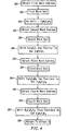
- Fig. 4 is a flow chart illustrating one cycle of a method for image format conversion according to the invention.
- the circuit in which the invention is implemented obtains the address for the first word (first pixel) of the chunky data (200). In the example, this word address is offset 0.
- the processor sends this first word via the processor interface to the circuit in which the invention is implemented (205).
- the barrel shifter in the circuit does not shift the word (210).
- the word C 0 M 0 Y 0 K 0 is therefore separated into four bytes. Referring to Fig. 3, byte C 0 is transferred to memory cell 50, byte M 0 to memory cell 52, byte Y 0 to memory cell 54, and byte K 0 to memory cell 56.
- the circuit then obtains the address for the second word (second pixel) of the chunky data (215).
- this word address is offset +1 Word (+4 bytes).
- the processor sends this second word via the processor interface to the circuit (220).
- the barrel shifter shifts each of the bytes in the word one position (225).
- the word K 1 C 1 M 1 Y 1 is therefore separated into four bytes, with byte C 1 transferred to memory cell 50, byte M 1 to memory cell 52, byte Y 1 to memory cell 54, and byte K 1 to memory cell 56.
- the circuit next obtains the address for the third word (third pixel) of the chunky data (230), offset +2 Words (+8 bytes).
- the processor sends this third word via the processor interface to the circuit (235).
- the barrel shifter shifts each byte in the word two positions (240).
- the word Y 2 K 2 C 2 M 2 is separated into four bytes, with byte C 2 transferred to memory cell 50, byte M 2 to memory cell 52, byte Y 2 to memory cell 54, and byte K 2 to memory cell 56.
- the circuit then obtains the address for the fourth word (fourth pixel) of the chunky data (245), offset +3 Words (+12 bytes).
- the processor sends this fourth word via the processor interface to the circuit (250).
- the barrel shifter shifts each byte in the word three positions (255).
- the word C 3 M 3 Y 3 K 3 is separated into four bytes, with byte C 3 transferred to memory cell 50, byte M 3 to memory cell 52, byte Y 3 to memory cell 54, and byte K 3 to memory cell 56.
- next word address returns to offset 0 (260) and the process is repeated until all of the chunky data have been stored as planar data in the memory cells.
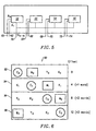
- Fig. 5 is a diagram illustrating memory cell addressing according to the invention.
- the lowest two address lines, A 0 and A 1 , of each memory cell 50, 52, 54, 56 are not interconnected with the address lines of any other memory cell.
- These "non-common" address lines function as a set of selection lines 60, 62, 64, 66, 68, 70, 72, 74 whose binary values determine the number of positions that the data to be stored in the memory cell are shifted. In this way, each byte in each color plane is stored in its proper position in relation to each other byte in the respective color plane.
- the remaining addresses 76, A 2 through A 10 in the example are interconnected. These addresses are used to store the bytes of each word as they are output from the barrel shifter.
- the barrel shifter does not shift the input data if the binary values (decimal equivalents are shown in parenthesis) stored in A 0 and A 1 of memory cells 50, 52, 54, and 56 are "00" (zero), “01” (one), “10” (two), and “11” (three), respectively.
- the barrel shifter to rotates the input data once if the stored binary values are "11” (three), “00” (zero), "01” (one), and “10” (two), respectively.
- Table 1 is a function table for the four-byte barrel shifter of the preferred embodiment of the invention.
- Memory Cell 50 52 54 56 No shift "00" (0) “01” (1) "10” (2) “11” (3) Rotate once “11” (3) “00” (0) “01” (1) "10” (2) Rotate twice “10” (2) “11” (3) “11” (0) “01” (1) Rotate three times “01” (1) "10” (2) "11” (3) "00” (0)
- the barrel shifter thereby sorts the input chunky format data by color plane to output planar format data.
- these data are output via the PCI interface 42 to a printer (not shown) via four lines 76, 80, 82, 84 of the PCI data bus.
- Fig. 6 is a diagram that shows color plane byte shifting for four pixels according to the invention.
- a portion of an image 90 is stored in chunky format.
- Each word 92, 94, 96, 98 contains bytes for each of the four color planes.
- the bytes for each word are identified by a subscript.
- the magenta byte of the first word 92 is denoted M 0 and the magenta byte for the third word 16 is M 2 .
- the cyan bytes C 0 , C 1 , C 2 , C 3 are separated when the input data are not shifted.
- the magenta bytes M 0 , M 1 , M 2 , M 3 are separated next, followed by the yellow and black bytes.
- the separated bytes are then output from the barrel shifter.
- the barrel shifter thus receives chunky data as an input, and outputs the data in planar format.
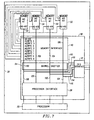
- Fig. 7 is a block schematic diagram showing operation of a barrel shifter for a cyan color separation according to the invention. The following discussion is best understood if Fig. 6 is also consulted.
- the barrel shifter 34 does not shift the input data in accordance with the binary values on the memory selection lines. These values are shown on Fig. 7 as "00" at memory cell 50, "10” at memory cell 52, "01” at memory cell 54, and "11" at memory cell 56.
- byte C 0 from the first word is transmitted on line 118 to the barrel shifter.
- the byte is output from the barrel shifter on line 100 to memory cell 50.
- Byte C 1 from the second word is transmitted on line 120 to the barrel shifter.
- the byte is output from the barrel shifter on line 102 to memory cell 52.
- byte C 2 from the third word, is transmitted on line 122 to the barrel shifter.
- the byte is output from the barrel shifter on line 104 to memory cell 54.
- Byte C 3 from the fourth word, is transmitted on line 124 to the barrel shifter.
- the byte is output from the barrel shifter on line 104 to memory cell 56.
- the cyan color plane is assembled from the chunky image data for output to the printer ( e.g. via the PCI interface) in a planar format.
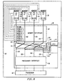
- Fig. 8 is a block schematic diagram showing operation of the barrel shifter for a magenta color separation according to the invention.
- input data are shifted one position by the barrel shifter, as shown by the selection line values at memory cells 50 "11", 52 ("00", 54 ("10"), and 56 ("01").
- byte M 0 from the first word is transmitted on line 118 to the barrel shifter, and output from the barrel shifter on line 102 to memory cell 52.
- Byte M 1 from the second word is transmitted on line 120, and output from the barrel shifter on line 104 for storage in memory cell 54.
- Byte M 2 from the third word is transmitted on line 122, and output from the barrel shifter on line 106 for storage in memory cell 56.
- Byte M 3 from the fourth word is transmitted on line 124 to the barrel shifter, and output from on line 100 to memory cell 50.
- Fig. 9 is a block schematic diagram showing operation of the barrel shifter for a yellow color separation according to the invention.
- input data are shifted two positions by the barrel shifter, as shown by the selection line values at memory cells 50 ("01"), 52 ("11"), 54 ("00"), and 50 ("10").
- byte Y 0 from the first word is transmitted on line 118 to the barrel shifter, and output from the barrel shifter on line 104 to memory cell 54.
- Byte Y 1 from the second word is transmitted on line 120, and output from the barrel shifter on line 106 for storage in memory cell 56.
- Byte Y 2 from the third word is transmitted on line 122, and output from the barrel shifter on line 100 for storage in memory cell 50.
- Byte Y 3 from the fourth word is transmitted on line 124 to the barrel shifter, and output from on line 102 to memory cell 52.
- Fig. 10 is a block schematic diagram showing operation of the barrel shifter for a black color separation according to the invention.
- input data are shifted three positions by the barrel shifter, as shown by the selection line values at memory cells 50 ("10"), 52 ("01"), 54 ("11"), and 56 ("00").
- byte K 0 from the first word is transmitted on line 118 to the barrel shifter, and output from the barrel shifter on line 106 to memory cell 56.
- Byte K 1 from the second word is transmitted on line 120, and output from the barrel shifter on line 100 for storage in memory cell 50.
- Byte K 2 from the third word is transmitted on line 122, and output from the barrel shifter on line 102 for storage in memory cell 52.
- Byte K 3 from the fourth word is transmitted on line 124 to the barrel shifter, and output from on line 104 to memory cell 54.
- color-sorted bytes in planar format may be input from the print buffer to the barrel shifter.
- the barrel shifter is then used to sort the planar bytes to output the image data in a chunky format. This is readily accomplished, for example, by reconfiguring the memory cell select lines accordingly.
- the invention may be used with any color conversion scheme that generates a CMYK image.
- the invention may be used when the image is rendered from a HSV (hue, saturation, value) color cone image or an RGB image to a CMYK image. Accordingly, the invention should only be limited by the Claims included below.
Landscapes
- Physics & Mathematics (AREA)
- General Physics & Mathematics (AREA)
- Engineering & Computer Science (AREA)
- Theoretical Computer Science (AREA)
- Record Information Processing For Printing (AREA)
- Color Image Communication Systems (AREA)
- Image Processing (AREA)
- Color Television Systems (AREA)
- Apparatus For Radiation Diagnosis (AREA)
- Facsimile Image Signal Circuits (AREA)
- Image Input (AREA)
Abstract
Description
| Memory Cell: | 50 | 52 | 54 | 56 |
| No shift | "00" (0) | "01" (1) | "10" (2) | "11" (3) |
| Rotate once | "11" (3) | "00" (0) | "01" (1) | "10" (2) |
| Rotate twice | "10" (2) | "11" (3) | "11" (0) | "01" (1) |
| Rotate three times | "01" (1) | "10" (2) | "11" (3) | "00" (0) |
Claims (9)
- A method for converting image data comprising a plurality of bytes in a chunky format to a planar format, the method comprising:providing a plurality of memory cells having an interconnected address;receiving the bytes in chunky format;separating each of the received bytes by color plane with a barrel shifter;storing the separated bytes in the memory cells; andseparately outputting the separated bytes of each color plane from the barrel shifter to provide planar format image data.
- The method of Claim 1, further comprising:rendering the image data in chunky data format in a processor, the processor comprising a bus; andtransmitting the chunky data over the bus to the barrel shifter.
- The method of Claim 1, wherein each of the memory cells comprises two addresses that are not interconnected to the addresses of other memory cells.
- The method of Claim 3, wherein the barrel shifter separates the received bytes according to binary values provided at the two non-interconnected addresses.
- The method of Claim 4, wherein the barrel shifter outputs cyan bytes when the barrel shifter does not shift byte position in response to the binary values.
- The method of Claim 4, wherein the barrel shifter outputs magenta bytes when the barrel shifter shifts bytes one position in response to the binary values.
- The method of Claim 4, wherein the barrel shifter outputs yellow bytes when the barrel shifter shifts bytes two positions in response to the binary values.
- The method of Claim 4, wherein the barrel shifter outputs black bytes when the barrel shifter shifts bytes three positions in response to the binary values.
- The method of Claim 1, further comprising:providing the separated bytes to the barrel shifter; and using the barrel shifter to sort the separated bytes to output the image in chunky format.
Applications Claiming Priority (3)
| Application Number | Priority Date | Filing Date | Title |
|---|---|---|---|
| US900085 | 1997-07-24 | ||
| US08/900,085 US6348978B1 (en) | 1997-07-24 | 1997-07-24 | Method and system for image format conversion |
| PCT/US1998/014073 WO1999005650A1 (en) | 1997-07-24 | 1998-07-01 | Method and system for image format conversion |
Publications (2)
| Publication Number | Publication Date |
|---|---|
| EP0996934A1 EP0996934A1 (en) | 2000-05-03 |
| EP0996934B1 true EP0996934B1 (en) | 2004-03-24 |
Family
ID=25411951
Family Applications (1)
| Application Number | Title | Priority Date | Filing Date |
|---|---|---|---|
| EP98934301A Expired - Lifetime EP0996934B1 (en) | 1997-07-24 | 1998-07-01 | Method and system for image format conversion |
Country Status (10)
| Country | Link |
|---|---|
| US (1) | US6348978B1 (en) |
| EP (1) | EP0996934B1 (en) |
| JP (1) | JP2001511612A (en) |
| AT (1) | ATE262712T1 (en) |
| AU (1) | AU722868B2 (en) |
| BR (1) | BR9811534A (en) |
| CA (1) | CA2293613A1 (en) |
| DE (1) | DE69822634T2 (en) |
| IL (1) | IL133459A0 (en) |
| WO (1) | WO1999005650A1 (en) |
Families Citing this family (18)
| Publication number | Priority date | Publication date | Assignee | Title |
|---|---|---|---|---|
| US6957307B2 (en) * | 2002-03-22 | 2005-10-18 | Intel Corporation | Mapping data masks in hardware by controller programming |
| US9411431B2 (en) * | 2006-12-29 | 2016-08-09 | Marvell World Trade Ltd. | Tracking a position in relation to a surface |
| US8226194B1 (en) | 2007-01-02 | 2012-07-24 | Marvell International Ltd. | Printing on planar or non-planar print surface with handheld printing device |
| US8077343B1 (en) | 2007-01-03 | 2011-12-13 | Marvell International Ltd. | Determining end of print job in handheld image translation device |
| US7949370B1 (en) | 2007-01-03 | 2011-05-24 | Marvell International Ltd. | Scanner for a mobile device |
| US8632266B1 (en) | 2007-01-03 | 2014-01-21 | Marvell International Ltd. | Printer for a mobile device |
| US8472066B1 (en) | 2007-01-11 | 2013-06-25 | Marvell International Ltd. | Usage maps in image deposition devices |
| US8342627B1 (en) | 2007-01-11 | 2013-01-01 | Marvell International Ltd. | Adaptive filtering scheme in handheld positioning device |
| US8396654B1 (en) | 2007-01-18 | 2013-03-12 | Marvell International Ltd. | Sensor positioning in handheld image translation device |
| EP2114688A1 (en) * | 2007-02-23 | 2009-11-11 | Marvell World Trade Ltd | Determining positioning of a handheld image translation device |
| US8223384B1 (en) * | 2007-02-23 | 2012-07-17 | Marvell International Ltd. | Defining a print image in memory for handheld image translation devices |
| US8351062B2 (en) * | 2007-02-26 | 2013-01-08 | Marvell World Trade Ltd. | Bit selection from print image in memory of handheld image translation device |
| US8096713B1 (en) | 2007-03-02 | 2012-01-17 | Marvell International Ltd. | Managing project information with a hand-propelled device |
| WO2008109557A1 (en) * | 2007-03-02 | 2008-09-12 | Marvell World Trade Ltd. | Dynamic image dithering |
| CN101675655B (en) * | 2007-03-02 | 2013-06-05 | 马维尔国际贸易有限公司 | Position correction for handheld printer |
| US9180686B1 (en) | 2007-04-05 | 2015-11-10 | Marvell International Ltd. | Image translation device providing navigational data feedback to communication device |
| US9555645B1 (en) | 2007-08-07 | 2017-01-31 | Marvell International Ltd. | Controlling a plurality of nozzles of a handheld printer |
| US8917336B2 (en) * | 2012-05-31 | 2014-12-23 | Apple Inc. | Image signal processing involving geometric distortion correction |
Family Cites Families (14)
| Publication number | Priority date | Publication date | Assignee | Title |
|---|---|---|---|---|
| US4058828A (en) | 1975-05-27 | 1977-11-15 | Eastman Kodak Company | Document copying apparatus |
| EP0277962A1 (en) | 1986-07-18 | 1988-08-17 | Sigmex Limited | Raster-scan graphical display apparatus |
| US5046023A (en) * | 1987-10-06 | 1991-09-03 | Hitachi, Ltd. | Graphic processing system having bus connection control capable of high-speed parallel drawing processing in a frame buffer and a system memory |
| US4914622A (en) | 1987-04-17 | 1990-04-03 | Advanced Micro Devices, Inc. | Array-organized bit map with a barrel shifter |
| US4983958A (en) | 1988-01-29 | 1991-01-08 | Intel Corporation | Vector selectable coordinate-addressable DRAM array |
| US5005011A (en) | 1988-12-23 | 1991-04-02 | Apple Computer, Inc. | Vertical filtering apparatus for raster scanned display |
| US4953104A (en) | 1989-05-18 | 1990-08-28 | Eastman Kodak Company | Page buffer for an electronic gray-scale color printer |
| US5162788A (en) | 1989-06-16 | 1992-11-10 | Apple Computer, Inc. | Chunky planar data packing apparatus and method for a video memory |
| US5269003A (en) | 1990-05-24 | 1993-12-07 | Apple Computer, Inc. | Memory architecture for storing twisted pixels |
| JP3110746B2 (en) * | 1990-10-09 | 2000-11-20 | キヤノン株式会社 | Image processing method |
| US5440329A (en) * | 1991-09-18 | 1995-08-08 | Tektronix, Inc. | Systems and methods for thermal transfer printing |
| US5168552A (en) | 1991-10-29 | 1992-12-01 | Hewlett-Packard Company | Color separation in ink jet color graphics printing |
| US5452235A (en) | 1993-11-01 | 1995-09-19 | Intel Corp. | Planar/packed video data FIFO memory device |
| US5768481A (en) * | 1995-06-05 | 1998-06-16 | Apple Computer, Inc. | Method and apparatus for compression of digitized image data using a dynamic band recompression scheme |
-
1997
- 1997-07-24 US US08/900,085 patent/US6348978B1/en not_active Expired - Lifetime
-
1998
- 1998-07-01 EP EP98934301A patent/EP0996934B1/en not_active Expired - Lifetime
- 1998-07-01 AT AT98934301T patent/ATE262712T1/en not_active IP Right Cessation
- 1998-07-01 WO PCT/US1998/014073 patent/WO1999005650A1/en not_active Ceased
- 1998-07-01 AU AU83857/98A patent/AU722868B2/en not_active Ceased
- 1998-07-01 DE DE69822634T patent/DE69822634T2/en not_active Expired - Fee Related
- 1998-07-01 JP JP2000504554A patent/JP2001511612A/en active Pending
- 1998-07-01 CA CA002293613A patent/CA2293613A1/en not_active Abandoned
- 1998-07-01 BR BR9811534-0A patent/BR9811534A/en not_active IP Right Cessation
- 1998-07-01 IL IL13345998A patent/IL133459A0/en unknown
Also Published As
| Publication number | Publication date |
|---|---|
| WO1999005650A1 (en) | 1999-02-04 |
| EP0996934A1 (en) | 2000-05-03 |
| DE69822634T2 (en) | 2005-03-31 |
| ATE262712T1 (en) | 2004-04-15 |
| BR9811534A (en) | 2000-08-29 |
| CA2293613A1 (en) | 1999-02-04 |
| JP2001511612A (en) | 2001-08-14 |
| US6348978B1 (en) | 2002-02-19 |
| AU8385798A (en) | 1999-02-16 |
| DE69822634D1 (en) | 2004-04-29 |
| AU722868B2 (en) | 2000-08-10 |
| IL133459A0 (en) | 2001-04-30 |
Similar Documents
| Publication | Publication Date | Title |
|---|---|---|
| US6348978B1 (en) | Method and system for image format conversion | |
| US8134573B2 (en) | Encoding CMYK data for display using indexed RGB | |
| US5838333A (en) | Image processing device and image processing method | |
| US5719956A (en) | Image processing apparatus with separate color conversion for CMY signals and K signal | |
| US5225911A (en) | Means for combining data of different frequencies for a raster output device | |
| JPH0371863A (en) | Page buffer system for electronic gray scale color printer | |
| US7034955B2 (en) | Using a processor enhanced memory module to accelerate hardcopy image processing within existing printer controller | |
| US5003494A (en) | Data storage system for an electronic color printer | |
| EP2109304A1 (en) | Color management method, module, and program product, and printer ussing said method | |
| JP2006121607A (en) | Image processing apparatus and method | |
| US5828815A (en) | High quality multilevel halftoning for color images with reduced memory requirements | |
| JP2830690B2 (en) | Image processing device | |
| US8054518B2 (en) | Color imaging devices, color imaging methods, and color separation methods | |
| US20030107577A1 (en) | Data processing system having a plurality of processors and executing a series of processings in a prescribed order | |
| US7463385B2 (en) | Color map selection | |
| US20040160619A1 (en) | Image processing apparatus and its method | |
| US5109272A (en) | Method of superimposing color images and color image processing apparatus | |
| JP3550979B2 (en) | Image processing device | |
| US11521302B2 (en) | Image processing apparatus and image processing method | |
| US5917993A (en) | Color image processing apparatus | |
| JP3427975B2 (en) | Printer control circuit, printer and print system | |
| EP0709012B1 (en) | High quality multilevel halftoning for colour images with reduced memory requirements | |
| US7304769B2 (en) | Color imaging devices, color image forming methods, and color image data processing methods | |
| JP3217432B2 (en) | Color image data processing method | |
| JPH11227263A (en) | Printing system, printing device, and printing control device |
Legal Events
| Date | Code | Title | Description |
|---|---|---|---|
| PUAI | Public reference made under article 153(3) epc to a published international application that has entered the european phase |
Free format text: ORIGINAL CODE: 0009012 |
|
| 17P | Request for examination filed |
Effective date: 20000112 |
|
| AK | Designated contracting states |
Kind code of ref document: A1 Designated state(s): AT BE CH CY DE DK ES FI FR GB GR IE IT LI LU MC NL PT SE |
|
| 17Q | First examination report despatched |
Effective date: 20020828 |
|
| GRAP | Despatch of communication of intention to grant a patent |
Free format text: ORIGINAL CODE: EPIDOSNIGR1 |
|
| GRAS | Grant fee paid |
Free format text: ORIGINAL CODE: EPIDOSNIGR3 |
|
| GRAA | (expected) grant |
Free format text: ORIGINAL CODE: 0009210 |
|
| AK | Designated contracting states |
Kind code of ref document: B1 Designated state(s): AT BE CH CY DE DK ES FI FR GB GR IE IT LI LU MC NL PT SE |
|
| PG25 | Lapsed in a contracting state [announced via postgrant information from national office to epo] |
Ref country code: LI Free format text: LAPSE BECAUSE OF FAILURE TO SUBMIT A TRANSLATION OF THE DESCRIPTION OR TO PAY THE FEE WITHIN THE PRESCRIBED TIME-LIMIT Effective date: 20040324 Ref country code: IT Free format text: LAPSE BECAUSE OF FAILURE TO SUBMIT A TRANSLATION OF THE DESCRIPTION OR TO PAY THE FEE WITHIN THE PRESCRIBED TIME-LIMIT;WARNING: LAPSES OF ITALIAN PATENTS WITH EFFECTIVE DATE BEFORE 2007 MAY HAVE OCCURRED AT ANY TIME BEFORE 2007. THE CORRECT EFFECTIVE DATE MAY BE DIFFERENT FROM THE ONE RECORDED. Effective date: 20040324 Ref country code: FI Free format text: LAPSE BECAUSE OF FAILURE TO SUBMIT A TRANSLATION OF THE DESCRIPTION OR TO PAY THE FEE WITHIN THE PRESCRIBED TIME-LIMIT Effective date: 20040324 Ref country code: CY Free format text: LAPSE BECAUSE OF FAILURE TO SUBMIT A TRANSLATION OF THE DESCRIPTION OR TO PAY THE FEE WITHIN THE PRESCRIBED TIME-LIMIT Effective date: 20040324 Ref country code: CH Free format text: LAPSE BECAUSE OF FAILURE TO SUBMIT A TRANSLATION OF THE DESCRIPTION OR TO PAY THE FEE WITHIN THE PRESCRIBED TIME-LIMIT Effective date: 20040324 Ref country code: BE Free format text: LAPSE BECAUSE OF FAILURE TO SUBMIT A TRANSLATION OF THE DESCRIPTION OR TO PAY THE FEE WITHIN THE PRESCRIBED TIME-LIMIT Effective date: 20040324 Ref country code: AT Free format text: LAPSE BECAUSE OF FAILURE TO SUBMIT A TRANSLATION OF THE DESCRIPTION OR TO PAY THE FEE WITHIN THE PRESCRIBED TIME-LIMIT Effective date: 20040324 |
|
| REG | Reference to a national code |
Ref country code: GB Ref legal event code: FG4D |
|
| REG | Reference to a national code |
Ref country code: CH Ref legal event code: EP |
|
| REG | Reference to a national code |
Ref country code: IE Ref legal event code: FG4D |
|
| REF | Corresponds to: |
Ref document number: 69822634 Country of ref document: DE Date of ref document: 20040429 Kind code of ref document: P |
|
| PG25 | Lapsed in a contracting state [announced via postgrant information from national office to epo] |
Ref country code: SE Free format text: LAPSE BECAUSE OF FAILURE TO SUBMIT A TRANSLATION OF THE DESCRIPTION OR TO PAY THE FEE WITHIN THE PRESCRIBED TIME-LIMIT Effective date: 20040624 Ref country code: GR Free format text: LAPSE BECAUSE OF FAILURE TO SUBMIT A TRANSLATION OF THE DESCRIPTION OR TO PAY THE FEE WITHIN THE PRESCRIBED TIME-LIMIT Effective date: 20040624 Ref country code: DK Free format text: LAPSE BECAUSE OF FAILURE TO SUBMIT A TRANSLATION OF THE DESCRIPTION OR TO PAY THE FEE WITHIN THE PRESCRIBED TIME-LIMIT Effective date: 20040624 |
|
| PG25 | Lapsed in a contracting state [announced via postgrant information from national office to epo] |
Ref country code: LU Free format text: LAPSE BECAUSE OF NON-PAYMENT OF DUE FEES Effective date: 20040701 Ref country code: IE Free format text: LAPSE BECAUSE OF NON-PAYMENT OF DUE FEES Effective date: 20040701 |
|
| PG25 | Lapsed in a contracting state [announced via postgrant information from national office to epo] |
Ref country code: ES Free format text: LAPSE BECAUSE OF FAILURE TO SUBMIT A TRANSLATION OF THE DESCRIPTION OR TO PAY THE FEE WITHIN THE PRESCRIBED TIME-LIMIT Effective date: 20040705 |
|
| PG25 | Lapsed in a contracting state [announced via postgrant information from national office to epo] |
Ref country code: MC Free format text: LAPSE BECAUSE OF NON-PAYMENT OF DUE FEES Effective date: 20040731 |
|
| REG | Reference to a national code |
Ref country code: CH Ref legal event code: PL |
|
| ET | Fr: translation filed | ||
| PLBE | No opposition filed within time limit |
Free format text: ORIGINAL CODE: 0009261 |
|
| STAA | Information on the status of an ep patent application or granted ep patent |
Free format text: STATUS: NO OPPOSITION FILED WITHIN TIME LIMIT |
|
| 26N | No opposition filed |
Effective date: 20041228 |
|
| REG | Reference to a national code |
Ref country code: IE Ref legal event code: MM4A |
|
| PG25 | Lapsed in a contracting state [announced via postgrant information from national office to epo] |
Ref country code: PT Free format text: LAPSE BECAUSE OF NON-PAYMENT OF DUE FEES Effective date: 20040824 |
|
| PGFP | Annual fee paid to national office [announced via postgrant information from national office to epo] |
Ref country code: DE Payment date: 20080722 Year of fee payment: 11 |
|
| PGFP | Annual fee paid to national office [announced via postgrant information from national office to epo] |
Ref country code: NL Payment date: 20080716 Year of fee payment: 11 Ref country code: FR Payment date: 20080715 Year of fee payment: 11 |
|
| PGFP | Annual fee paid to national office [announced via postgrant information from national office to epo] |
Ref country code: GB Payment date: 20080722 Year of fee payment: 11 |
|
| GBPC | Gb: european patent ceased through non-payment of renewal fee |
Effective date: 20090701 |
|
| NLV4 | Nl: lapsed or anulled due to non-payment of the annual fee |
Effective date: 20100201 |
|
| REG | Reference to a national code |
Ref country code: FR Ref legal event code: ST Effective date: 20100331 |
|
| PG25 | Lapsed in a contracting state [announced via postgrant information from national office to epo] |
Ref country code: FR Free format text: LAPSE BECAUSE OF NON-PAYMENT OF DUE FEES Effective date: 20090731 |
|
| PG25 | Lapsed in a contracting state [announced via postgrant information from national office to epo] |
Ref country code: GB Free format text: LAPSE BECAUSE OF NON-PAYMENT OF DUE FEES Effective date: 20090701 |
|
| PG25 | Lapsed in a contracting state [announced via postgrant information from national office to epo] |
Ref country code: DE Free format text: LAPSE BECAUSE OF NON-PAYMENT OF DUE FEES Effective date: 20100202 |
|
| PG25 | Lapsed in a contracting state [announced via postgrant information from national office to epo] |
Ref country code: NL Free format text: LAPSE BECAUSE OF NON-PAYMENT OF DUE FEES Effective date: 20100201 |