EP0995193B1 - Semi-manufactured stamper and method of manufacturing the same - Google Patents
Semi-manufactured stamper and method of manufacturing the same Download PDFInfo
- Publication number
- EP0995193B1 EP0995193B1 EP98934101A EP98934101A EP0995193B1 EP 0995193 B1 EP0995193 B1 EP 0995193B1 EP 98934101 A EP98934101 A EP 98934101A EP 98934101 A EP98934101 A EP 98934101A EP 0995193 B1 EP0995193 B1 EP 0995193B1
- Authority
- EP
- European Patent Office
- Prior art keywords
- stamper
- semi
- manufactured
- layer
- manufactured stamper
- Prior art date
- Legal status (The legal status is an assumption and is not a legal conclusion. Google has not performed a legal analysis and makes no representation as to the accuracy of the status listed.)
- Revoked
Links
Images







Classifications
-
- G—PHYSICS
- G11—INFORMATION STORAGE
- G11B—INFORMATION STORAGE BASED ON RELATIVE MOVEMENT BETWEEN RECORD CARRIER AND TRANSDUCER
- G11B7/00—Recording or reproducing by optical means, e.g. recording using a thermal beam of optical radiation by modifying optical properties or the physical structure, reproducing using an optical beam at lower power by sensing optical properties; Record carriers therefor
- G11B7/24—Record carriers characterised by shape, structure or physical properties, or by the selection of the material
- G11B7/26—Apparatus or processes specially adapted for the manufacture of record carriers
-
- G—PHYSICS
- G11—INFORMATION STORAGE
- G11B—INFORMATION STORAGE BASED ON RELATIVE MOVEMENT BETWEEN RECORD CARRIER AND TRANSDUCER
- G11B7/00—Recording or reproducing by optical means, e.g. recording using a thermal beam of optical radiation by modifying optical properties or the physical structure, reproducing using an optical beam at lower power by sensing optical properties; Record carriers therefor
- G11B7/24—Record carriers characterised by shape, structure or physical properties, or by the selection of the material
- G11B7/26—Apparatus or processes specially adapted for the manufacture of record carriers
- G11B7/261—Preparing a master, e.g. exposing photoresist, electroforming
Definitions
- the present invention relates to methods of providing a semi-manufactured optical disc stamper.
- the invention also relates to such a stamper in combination with a protective package.
- the invention also relates to a process for manufacturing an optical disc by means of a structured stamper of the invention.
- Optical Discs such as compact discs (CD), digital video discs or digital versatile discs (DVD) and optically readable memories such as CD-ROM's are manufactured with the use of an injection moulding machine.
- the injection moulding machine comprises an injection moulding tool which determines the shape of the disc to be manufactured.
- a tool comprises a stamper having a pattern of protrusions to be imprinted on the disc.
- the pattern of the stamper is a model for information to be imprinted in the disc to be manufactured.
- a manufacturer of optical discs having an amount of information-to-be-replicated such as for example a music recording or computer data, needs to obtain a stamper with a pattern corresponding to that information.
- a stamper is manufactured in the following way: Firstly, a master having a pattern corresponding to the pattern to be on the Optical Discs is manufactured. Secondly the master is used for producing the stamper, such that the pattern of the stamper is the mirror image of the pattern of the master.
- each of the two steps “manufacturing a master”, and “manufacturing a stamper with the use of the master” in itself comprises a number of steps.
- the manufacture of a master involves (1) coating a smooth glass plate with a photosensitive material, and thereafter (2) curing the photoresist before (3) radiating the surface of the coated glass plate with a modulated laser to record a spiral track of information in the photoresist material.
- the areas designated to become pits are exposed to laser light.
- the master glass plate is subjected to an etching process (4) leading to the illuminated areas, i.e. the pits-to-be, being etched out such that a pattern of pits is generated.
- the surface of the master glass plate is made structured.
- the patterned, i.e. structured, surface of the plate is metallized (6), e.g. by vacuum deposition or sputtering of a thin conductive layer.
- the resulting multilayer construction (having a glass layer, a structured photoresist layer and a thin structured conductive layer) constitutes the master.
- the step of generating a stamper with the use of the master involves (1) deposition of nickel by electroplating, and (2) removal of the resulting nickel plate from the master.
- This removal step commonly results in a nickel plate having traces of photoresist and silver on the patterned surface, due to strong adhesion between the nickel and the conductive layer of the master. Hence the information carrying part of the master is destroyed in the process of making the stamper.
- the prior art process of making a stamper also involves a cleaning process (3) for removing any traces of photoresist and/or silver from the patterned surface of the nickel plate. Thereafter the opposite side of the nickel plate is commonly polished, a centre opening is punched out and an outer diameter punch is used to make the plate circular. At that stage a stamper suitable for use for mass production of information carrying optical discs has been obtained. Sometimes, however, an error occurs during one of the steps causing the obtained master and/or stamper to have substandard quality. Such a master or stamper will have to be rejected.
- a manufacturer of optical discs needs to perform a long process starting with a master, providing a structure on the master, and then creating a structured stamper with use of the master before the replication of optical discs can be initiated.
- This method requires a large amount of complex machinery to be installed at the premises of the manufacturer of optical discs - a machinery which also has to be handled by skilled personnel. Since the process consists of a large number of steps, it is also time consuming.
- some manufacturers of optical discs delivers the information-to-be-replicated to a third party.
- the third party then manufactures a structured stamper in accordance with the above described method and delivers it to the manufacturer of optical discs. This simplifies the procedure for the manufacturer of optical discs, but the total complexity of the method increases, and the time required for obtaining the information carrying stamper is relatively long.
- JP-A-3 225 646 and EP-A-0 495 281 disclose stampers having information pits and thus lacking unstructured portions on the guide tracks.
- EP-A-0 446 967 neither discloses unstructured portions for the application of a photosensitive layer.
- a problem to which the present invention is directed is to enable a manufacturer of optical discs to reduce the mean time duration from reception of information-to-be-replicated, such as for example a music recording or computer data, until successful replication of optical discs recorded with that information.
- Another problem to which the present invention is directed is to simplify the manufacture of a structured stamper. More precisely, the problem is to enable a manufacturer of optical discs to obtain a stamper provided with a selectable structure by means of an uncomplicated and cost-effective method.
- Yet another problem to be addressed by the invention is to enable a Manufacturer of Optical Discs to provide a structure on a blank stamper by means of an uncomplicated and cost-effective method, and without requiring complex machinery.
- Such a blank stamper means can be manufactured without having access to the in-formation-to-be-replicated.
- the blank stamper means can be manufactured without consideration to the pattern or structure to be formed in the Optical-Discs-to-be.
- An inspection of the unexposed semi-manufactured stamper is carried out after applying and drying the sensitive layer. Any semi-manufactured, blank, stampers which are of inferior quality prior to the step of enclosing it in the package, will be rejected. The rejected semi-manufactured stampers will not be packed. Only high-quality blank stampers, which pass the inspection will be enclosed in the package.
- the above described method provides the invention with the advantage of enabling an uncomplicated manufacture of a structured stamper.
- a blank stamper of the invention is transformable into a structured stamper by means of an advantageously uncomplicated method, thereby enabling a manufacturer of optical discs to obtain a stamper provided with a selectable structure by means of a quick and cost-effective method.
- the yield is improved, i.e. the rejection rate is decreased, since a number of critical manufacturing steps are performed prior to structuring the stamper means. Items that are rejected in the manufacturing steps before structuring will never be delivered to the Manufacturer of Optical Discs, and therefore does not affect the rejection rate as experienced by the Manufacturer of Optical Discs.
- the guide track provided on the blank stamper reduces the rejection rate in the structuring step by eliminating, or reducing, erroneous positioning of the information structure on the stamper.
- the guide track also enables use of a less complex, and therefore less costly, mastering equipment, while enabling the meeting of narrow tolerance specifications in the positioning of information.
- Data, i.e. a pattern of protrusions or indentations, on an Optical Disc needs to be provided in a predetermined manner along a substantially spiral line from one perimeter of the disc towards another perimeter of the disc. In order to maximize the information storage capacity and in order to enable accurate retrieval of the stored information, the spiral line of information needs to be provided within a narrow tolerance zone.
- the manufacturer-of-optical-discs starts out with a high-quality semi-manufactured stamper, which is already adapted for fitting into his injection moulding machine, the number of steps to be performed by the manufacturer-of-optical-discs is advantageously low. This leads to a high yield in that process.
- the process of manufacturing an optical disc is simplified and becomes less costly since, according to an embodiment of the invention, the process for manufacturing an optical disc comprises the steps set forth in claim 15.
- the invention also relates to a semi-manufactured stamper in combination with a protective package, as defined in claims 16 - 18.
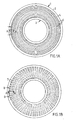
- Figure 1A is a top view of a blank stamper according to a first embodiment of the invention.
- Figure 1B is a top view of the stamper according to Fig 1A after structuring.
- Figure 2A is a flow chart illustrating a process of obtaining a blank stamper according to Figure 1A.
- Figure 2B is a flow chart illustrating a process of obtaining a structured stamper according to Figure 1B.
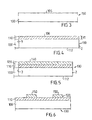
- Figure 3 is a schematic side view of a part of a plate to be used for manufacturing a stamper.
- Figure 4 is a schematic sectional side view of a part of a work piece for a blank stamper means according an embodiment of the invention.
- Figure 5 is a schematic sectional side view of the work piece shown in Figure 4, additionally including a layer sensitive to irradiation.
- Figure 6 is a schematic sectional side view of the work piece means according to Fig. 5, after the creation of a guide pattern in the exposure sensitive layer.
- Figure 7 is a schematic sectional side view of a blank stamper obtained from the work piece shown in Figure 6 by subjecting it to etching.
- Figure 8 is a schematic sectional side view of the blank stamper shown in Figure 7, after provision of an exposure sensitive material.
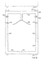
- Figure 9 is a sectional top view of a package 300 for a plurality of blank stampers 1.
- Figure 10 is a sectional side view of the package shown in Fig 9.
- Figure 11 is a schematic sectional side view of a the blank stamper shown in Figure 8, after exposing a pattern of information into the exposure sensitive material.
- Figure 12 is a sectional side view of a the blank stamper shown in Figure 11, after removal of unexposed material.
- Figure 13 is a sectional side view of a the blank stamper shown in Figure 12, after etching
- Figure 14 is a schematic sectional side view of a part of a stamper workpiece according to a further embodiment of the invention.
- Figure 15 is a schematic sectional side view of a blank stamper obtained from the work piece shown in Figure 14.
- Figure 16 is a schematic sectional side view of the blank stamper shown in Figure 15, after provision of an exposure sensitive material.
- Figure 17 is a sectional side view of a portion of a structured stamper 250 obtained from a blank stamper 1 as shown in Figs 15 or 16.
- Figure 18A is a flow chart illustrating a second embodiment of a process of obtaining a blank stamper as shown in Figure 1A.
- Figure 19 is a schematic sectional side view of a work piece including a layer sensitive to irradiation.
- Figure 20 is a schematic sectional side view of the work piece according to Fig. 19, after the creation of a guide pattern in the exposure sensitive layer.
- Figure 21 is a schematic sectional side view of the work piece according to Fig. 20, after provision of a guide track by ion etching.
- Figure 22 is a schematic sectional side view of the work piece according to Fig. 21, after removal of the exposure sensitive layer.
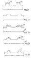
- Figure 23 is a schematic sectional side view of the work piece according to Fig. 22, after provision of an exposure sensitive mask film
- Figure 24 is a schematic sectional side view of the work piece according to Fig. 23, after exposing and curing the mask film in a first manner.
- Figure 25 is a schematic sectional side view of the structured stamper according to Fig. 24, after ion etching so as to achieve an information pattern in the stamper means
- Figure 26 is a schematic sectional side view of the work piece according to Fig. 23, after exposing and curing the mask film in a second manner.
- Figure 27 is a schematic sectional side view of the work piece according to Fig. 26, after ion etching so as to achieve an information pattern in the stamper means when cured mask film remains after etching.
- Figure 28 is a schematic sectional side view of the structured stamper according to Fig. 27, after removing any remains of the mask film.
- Figure 29 is a top view of a part of the structured stamper according to Fig. 28, as seen in the direction of arrow C in Fig 28.
- Figure 1A is a schematic top view of a blank stamper 1 according to a first embodiment of the invention.
- the blank stamper 1 comprises a substantially disc-shaped plate member having an outer perimeter 2 and an inner perimeter 3. The inner perimeter forms an opening in the plate.
- the blank stamper 1 has a first surface 4.
- the first surface 4 is provided with a guide track 6.
- Figure 1B is a schematic top view of the stamper according to figure after structuring.
- the structured stamper 5 is provided with a plurality of protrusions or indentations 7 (schematically indicated with dots on the surface of the stamper in Fig. 1B) on the surface 4 to be facing a cavity in an injection moulding machine. These protrusions/indentations are positioned in a predetermined positional relation to the guide track 6.
- the purpose of the opening formed by inner perimeter 3 is to enable easy installation of the structured stamper 5 into an injection moulding machine having an injection inlet for molten resin in the center of the stamper.
- Figure 2A is a flow chart illustrating a process of obtaining a blank stamper having a guide track as shown in Figure 1A.
- a workpiece 130 is selected (Fig 3).
- the workpiece 130 is to be worked into a blank stamper 1.
- a suitable workpiece comprises a plate 100 made from a material having a composition suitable for repetitive heat cycling and having a degree of hardness such that wear is minimized when used as a stamper for producing Optical Discs.
- the plate 100 is preferably a metal plate.
- the plate 100 (see Figure 3) is, according to an embodiment, a plate of nickel having a flat smooth surface 105.
- the plate 100 is, according to an embodiment, obtained by electroplating. Thereby an advantageously smooth surface 105 with a substantially glassy finish is provided. Alternatively a plate is treated such that a sufficiently smooth surface 105 is provided.
- a first layer 110 (see Figure 4) is provided on the surface 105 of the plate 100.
- the layer 110 is herein referenced to as a pattern layer, since a pattern is to be provided in the layer 110, as described below.
- the first layer 110 is provided by Physical Vapour Deposition, PVD. According to a preferred embodiment this is achieved by evaporation. According to another embodiment sputtering is used.
- the layer 110 is made of a material having a composition different from that of the plate 100 such that the layer 110 and the plate 100 have different sensitivity to a selected etchant.
- the properties of the layer 110 and the plate 100 are selected such that the layer 110 is etched well whereas the plate 100 is substantially insensitive to the selected etchant.
- the plate 100 comprises nickel, and the first layer 110 consists substantially of titanium nitride.
- Titanium nitride has the advantageous properties of being depositable by evaporation to a controllable layer thickness, and it stands temperature cycling very well plus it provides a durable surface.
- the temperature cycling endurance is an important aspect for a stamper since injection moulding involves repetitive heating and cooling.
- the first layer 110 can alternatively comprise silicon carbide, silicon nitride or wolfram carbide.
- the pattern layer 110 is made with a certain layer thickness d1.
- the thickness d1 corresponds to the desired height of protrusions 7 in the stamper 5 to be achieved.
- This height d1 should correspond to a depth d2 of the pits of the optical disc to be produced, and the configuration of the protrusions 7 should correspond to the configuration of the individual pits-to-be-obtained.
- the depth d2 of the pits in an optical disc manufactured with the stamper 5 should be about a quarter of the wave length of the laser used for reading the information from the optical disc.
- the layer thickness d1 is in the range 0.050 to 0.150 micrometer.
- a blank stamper has a pattern layer with a thickness in the range 0.100 to 0.130 micrometer, but preferably thinner than 0.125 micrometer. Such a blank stamper is suitable for transformation into a structured stamper for production of standard CD's.
- a blank stamper has a pattern layer with a thickness in the range 0.090 to 0.110 micrometer, or preferably 0.102 micrometer. Such a blank stamper is suitable for transformation into a structured stamper for production of optical video discs or DVD's.
- a blank stamper has a pattern layer 110 with a thickness in the range 0.062 to 0.082 micrometer, or preferably 0.072 micrometer.
- Such a blank stamper is suitable when the optical-disc-to-be-manufactured is to be used in a CD player having a laser working in the blue light wave length region.
- step S30 is an adaptation of the workpiece for the purpose of reducing the number of process steps to be performed by the end user of the stamper.
- the order of execution of steps S20 and S30 may be reversed. In fact, step S30 may be performed at any stage after step S10 but before placing the semi-manufactured stamper in a package for delivery (step S80 below).
- step S30 the workpiece is punched so as to provide a substantially circular outer perimeter 2 and an inner circular perimeter 3 of a smaller diameter (Fig. 1A).
- the punching is performed such that deformation of the workpiece is avoided.
- Machines for performing such punching are known to the person skilled in the art.
- the inner diameter is preferably between 25 mm and 38 mm, and the outer diameter is preferably between 125 mm and 150 mm.
- the resulting workpiece (Fig. 4) has a surface 106, an outer perimeter 2, an inner perimeter 3 and a back surface 112.
- the workpiece is a substantially stressfree, disc-shaped plate having a thickness of in the range 250 to 350 micrometer, preferably 300 micrometer.
- the surface 106 is structurable, but substantially unstructured.
- the quality of the surface 112 is of importance since the stamper-to-be must be substantially flat during the injecting moulding procedure. Due to the relatively small thickness of the stamper, the avoidance of surface irregularities of the back surface 112 are of great importance, since large surface irregularities may cause bulging of the stamper when mounted against a flat plane surface in the injection moulding machine and the high pressure in the moulding cavity during moulding presses the stamper against the flat plane machine surface. Such bulging would, in turn, lead to inferior quality of the resulting moulded product.
- step S30 also includes treatment of the surface 112 such that surface irregularities are minimized.
- This treatment includes polishing according to one version of the invention.
- the mean surface deviation R z provides a measure of the average deviation in a direction perpendicular to the plane of the surface.
- the surface 112 is treated to obtain a mean surface deviation value R z below 2,0 micrometer, since inferior quality of replicated optical disks is obtained when the mean surface deviation value R z exceeds 2,0 micrometer.
- the mean surface deviation R z of surface 112 after treatment is less than 1,0 micrometer.
- the maximum surface deviation R max is measured according to DIN 4768, and according to one embodiment the maximum surface deviation value R max is below 3,0 micrometer for the treated surface 112. According to a preferred embodiment R max has a value below 1,3 micrometer.
- the arithmetic average deviation R a is the arithmetic mean value of all distances from the surface profile to a mean surface line, each distance being measured perpendicularly to the mean surface line.
- the arithmetic average deviation R a is obtained by evaluation of the surface 112 along an evaluation line.
- the back surface is treated so as to obtain an arithmetic average surface deviation value R a below 0,3 micrometer or at least below 0,5 micrometer.
- R a has a value below 0.1 micrometer for the treated surface 112.
- the treatment of the back surface 112 should preferably be executed on the blank stamper before structuring it. Furthermore, it to be noted that every step in the treatment of a stamper has a rejection ratio, i.e. statistically a certain portion of the articles will fail the quality requirements after the treatment step. For these reasons it is advantageous to perform the treatment of the back surface on the blank stamper 1 before structuring it.
- a layer 120 sensitive to irradiation is applied on the first layer 110 (see Figure 5).
- the sensitive layer 120 is a mask film to be exposed and developed into a suitable mask pattern.
- the sensitive layer 120 is spin coated onto the surface 106 to a substantially even thickness.
- the term "sensitive layer” used in this text comprises sensitivity to electron beams as well as sensitivity to laser exposure.
- the sensitive layer is, in one version of the invention, a photosensitive resist film.
- the irradiation sensitivity of layer 120 is not limited to the above examples, but can be sensitivity to beams or rays of other irradiation such as for example X-rays or ultraviolet rays.
- the sensitive layer may be sensitive in a positive manner or in a negative manner.
- a positively sensitive layer When a positively sensitive layer is used the exposed areas are removed by the development process, described with reference to Fig. 2B below. Conversely, when a negatively sensitive layer is used the unexposed areas are removed by the development process.
- the workpiece resulting from step S40 ( Fig. 5) has a front surface 140, an outer edge and a back surface 112, the front surface 140 being structurable, but substantially unstructured.
- a subsequent step S50 the sensitive layer 120 is exposed to provide the pattern of a guide track. After development the resulting workpiece has a protruding spiral portion of cured remains of the sensitive layer 120 forming a mask 150, as shown in Fig. 6.
- Fig. 7 shows a cross-section taken along line A-A of the blank stamper embodiment in Fig. 1A.
- the guide track 6 is formed of an elongated protruding part of the structurable layer 110 having a surface area 106'.
- the surface area 106' is a portion of the surface 106 of the structurable layer 110.
- the workpiece is preferably prepared, shaped and adapted such that the only remaining processing, for obtaining a structured stamper ready for installation in an injection moulding machine, is to provide the information structure in the pattern layer 110.
- the blank stamper is additionally provided with an unexposed layer of an exposure sensitive layer 160, as shown in Fig. 8.
- the exposure sensitive layer 160 can be provided by spin coating a liquid onto the blank stamper shown in Fig. 7 and curing it (step S70).
- the cured layer 160 is unexposed and therefore ready to be radiated e.g. with a modulated laser to record a spiral track of information.
- FIG 18A is a flow chart illustrating a second embodiment of a process of obtaining a blank stamper having a guide track as shown in Figure 1A.
- a stamper workpiece 130 is selected (step S210). The workpiece is to be worked into a blank stamper 1.
- a suitable workpiece comprises a plate 100 made from a material having a composition suitable for repetitive heat cycling and having a degree of hardness such that wear is minimized when used as a stamper for producing Optical Discs (see Figure 3).
- the plate 100 may, according to this embodiment be a plate of nickel or of any suitable material having a flat smooth surface 105.
- the surface of the plate 100 is formed such that an advantageously smooth surface 105 with a substantially glassy finish is provided.
- a plate is treated such that a sufficiently smooth surface 105 is provided.
- the temperature cycling endurance is an important aspect for a stamper since injection moulding involves repetitive heating and cooling.
- the plate may also comprise a material such as e.g. silicon carbide, silicon nitride or wolfram carbide for a surface.
- the plate would then be in the form of a laminate. This plate, either being a solid piece or a laminate would however not be used in the same way as in the first embodiment.
- the plate is, in a step S230, provided with a layer 120, sensitive to irradiation on the plate surface 105 (see Figure 18A and 19).
- the sensitive layer 120 is a mask film to be exposed and developed into a suitable mask pattern.
- the sensitive layer 120 may spin coated onto the surface 105 to a substantially even thickness.
- the term "sensitive layer” used in this text comprises sensitivity to electron beams as well as sensitivity to laser exposure.
- the sensitive layer is, in one version of the invention, a photosensitive resist film.
- the irradiation sensitivity of layer 120 is not limited to the above examples, but can be sensitivity to beams or rays of other irradiation such as for example X-rays or ultraviolet rays.
- the sensitive layer may be sensitive in a positive manner or in a negative manner.
- a positively sensitive layer When a positively sensitive layer is used the exposed areas are removed by a development process. Conversely, when a negatively sensitive layer is used the unexposed areas are removed by a development process.
- the workpiece resulting from step S230 has a front surface 140, an outer edge and a back surface 112, the front surface 140 being structurable, but substantially unstructured.
- a subsequent step S240 the sensitive layer 120 is exposed to provide the pattern of a guide track. After development the resulting workpiece has a protruding spiral portion of cured remains of the sensitive layer 120 forming a mask 150, as shown in Fig. 20.
- step S250 The workpiece is thereafter (in step S250) subjected to ion machining, reactive ion etching, ion milling, plasma etching or the like. Such treatment is herein referred as ion etching.
- ion etching Such treatment is herein referred as ion etching.
- the process will leave land areas corresponding to the areas where the mask 150 is present and will remove material where there is no photoresist present thus giving the plate a spirally shaped guide track, as illustrated in Figs 21 and 22.
- This ion etching process gives a depth in the etched areas corresponding to a time parameter.
- the process also depends on gas pressure and other technical parameters which can be determined by the man skilled in the art without any inventive activity.
- the depth of the etched areas is dependent on the duration of the ion etching process i.e. the time parameter.
- the ion etching is continued until a depth d1 is reached.
- This depth d1 corresponds to the desired height of protrusions 7 in the stamper 5 to be achieved.
- This height d1 should correspond to a depth d2 of the pits of the optical disc to be produced, and the configuration of the protrusions 7 should correspond to the configuration of the individual pits-to-be-obtained.
- the depth d2 of the pits in an optical disc manufactured with the stamper 5 should be about a quarter of the wave length of the laser used for reading the information from the optical disc.
- the depth d1 is in the range 0.050 to 0.150 micrometer.
- a blank stamper is ion etched to a depth in the range 0.100 to 0.130 micrometer, but preferably less than 0.125 micrometer.
- Such a blank stamper is suitable for transformation into a structured stamper for production of standard CD's.
- a blank stamper is ion etched to a depth in the range 0.090 to 0.110 micrometer, or preferably 0.102 micrometer. Such a blank stamper is suitable for transformation into a structured stamper for production of optical video discs or DVD's.
- a blank stamper is ion etched to a depth in the range 0.062 to 0.082 micrometer, or preferably 0.072 micrometer.
- Such a blank stamper is suitable when the optical-disc-to-be-manufactured is to be used in a CD player having a laser working in the blue light wave length region.
- step S220 is an adaptation of the workpiece for the purpose of reducing the number of process steps to be performed by the end user of the stamper.
- step S220 may be performed at any stage after step S210 but before placing the semi-manufactured stamper in a package for delivery (step S270 below).
- step S220 the workpiece is punched so as to provide a substantially circular outer perimeter 2 and an inner circular perimeter 3 of a smaller diameter (Fig. 18A).
- the punching is performed such that deformation of the workpiece is avoided.
- Machines for performing such punching are known to the person skilled in the art.
- the inner diameter is preferably between 25 mm and 38 mm, and the outer diameter is preferably between 125 mm and 150 mm.
- the stamper provided with a spiral track is then provided with an irradiation sensitive mask film layer 270 (step S260), which may be exposed for recording information.
- Fig 23 illustrates a stamper provided with a spiral track having an irradiation sensitive mask film layer 270.
- a semi-manufactured stamper with a guide track is provided by electroplating.
- This embodiment involves coating a smooth glass plate with a photosensitive material, and thereafter curing the photoresist before radiating the surface of the coated glass plate with a modulated laser to record a spiral guide track in the photoresist material. Thereafter the master glass plate is subjected to an etching process leading to the illuminated areas being etched out such that a guide track is generated. In other words the surface of the master glass plate is made structured. After a drying process the surface of the plate is metallized, e.g. by vacuum deposition or sputtering of a thin conductive layer.
- the resulting multilayer construction (having a glass layer, a photoresist layer defining a guide track and a thin structured conductive layer) constitutes the master.
- the step of generating a semi-manufactured stamper with the use of the master involves deposition of nickel by electroplating, and removal of the resulting nickel plate from the master. This results in a blank stamper with a guide track, shown in Fig. 1, and similar to the one shown in Fig.7.
- the layer 160 being sensitive to irradiation, may present the problem of enabling transport of the blank stamper 1 without damaging it.
- the blank stamper 1 according to Fig. 8 is placed in a protective package, as illustrated by step S80 in Fig. 2A.
- the package comprises walls designed to prevent external irradiation from penetrating into a stored stamper.
- the blank stamper shown in Fig. 7 has vulnerable surfaces 105', 106' and 112, which must be protected from scratching during transport.
- the blank stamper is stored in a package devised to hold a plurality of blanks 1 such that the stamper surfaces are protected from being damaged.
- a package is illustrated in Fig. 9.
- Fig. 9 is a sectional top view of a package 300 for a plurality of blank stampers 1.
- the package comprises a housing 310 having inner walls 320.
- Two opposing inner walls 320 are provided at a predetermined distance from each other, and the walls are provided with shaped portions 330 for holding a blank stampers having an outer perimeter of a predetermined measure.
- the shaped portions are grooves adapted for allowing insertion of a blank stamper.
- Fig. 10 is a sectional side view of the package shown in Fig. 9.
- the package has an inner bottom wall 340 provided with recesses 350 adapted for receiving blank stampers.
- An openable/closable lid 360 has an inner wall 370 having means 380 for urging a stored stamper towards a corresponding recess 350.
- an inlet 390 for an anti-oxidant such as nitrogen.
- an outlet 400 so that a gas flow through the package can be obtained.
- the inlet and the outlet are provided with closable valves.
- the package is sealable by means of sealing means 410.
- the provision of blank stampers in a package has the advantage of enabling the manufacturer of optical discs to acquire blanks which are easily transformed into structured stampers ready for use in an injection moulding machine.
- Figure 2B is a flow chart illustrating a process of obtaining a structured stamper as illustrated in Figure 1B.
- the method includes the step of obtaining a blank stamper of the type shown in Fig. 8 (Step S110 in Fig. 2B).
- the acquisition of a blank stamper 1 may include unpacking a blank from a package.
- step S110 involves receiving a semi-manufactured stamper 1 having a guide track and an unexposed, exposable mask film 160, as illustrated in Fig. 8.
- step S110 involves: firstly, receiving a semi-manufactured stamper 1 having a guide track, as illustrated in Fig. 7, and secondly, providing an exposable mask film on structurable portions of the semi-manufactured stamper 1.
- the step S110 of obtaining a blank stamper includes all steps S10 - S70 as described above with reference to Fig. 2A.
- step S120 a pattern of protrusions 7 is created in the pattern layer 110, which yields the desired structured stamper 5 (see Figure 2B and 1B).
- a pattern of indentations are created in the layer 110.
- the pattern creating step S120 advantageously involves only a very limited number of steps to be performed.
- a pattern is created in the sensitive layer 160. This may be achieved by setting the blank 1 shown in Figures 1 and 5 in an exposure device, where a modulated laser beam is controlled to radiate parts 145 of the surface 140 of the photosensitive layer 120. In this manner a pattern of rounded and elongate surface areas are left unexposed on the workpiece 130.
- the pattern may include a spiral track of such exposed areas 145 on the photosensitive layer 120.
- Fig. 11 shows the blank stamper 1 after exposure.
- the exposure device needs to be accurately controlled to provide a densely packed amount of information on the stamper.
- the guide track 6' in the stamper 1 shown in Fig. 8 enables the use of a relatively uncomplicated exposure device.
- the blank stamper 1 is developed, i.e. the blank stamper 1 is treated such that the unexposed areas of the sensitive layer 120 are removed. This may be achieved by placing the blank stamper 1 in developing solution.
- the guide track 6 is provided with protrusions 160, as shown in Figure 12.
- a subsequent step S140 ( Figure 2B) the stamper 1 (see Figure 12) is treated in an etch process.
- Etching may be performed in a variety of different manners. It can for example be performed by dry etching methods or by use of a liquid etchant. It may also include ion etching, as discussed above.
- the semi-manufactured stamper 1 When etching with use of liquid etchant the semi-manufactured stamper 1 is placed in a bath with a liquid which reacts with the material at the exposed surface parts of the guide protrusion 6.
- the etching process is controlled such that the etching leaves protrusions 7 in the first layer 110 (see Figure 13).
- the plate 100 comprises nickel, and the first layer 110 consists substantially of titanium nitride.
- the etching liquid used in the etch process S60 is selected such that it acts on the first layer 110 but not on the plate 100.
- a subsequent step S150 ( Figure 2B) the remaining portions of the photosensitive layer 120 is removed, yielding a stamper surface with a pattern of protrusions 7, as illustrated in Figure 1B and 13.
- the thickness d1 of the layer 110 is predetermined by process step S20, and the plate 100 is not etchable by the etching solution, the depth of the indentations is substantially independent on the etching variables.
- the height h 1 of the protrusions in the stamper 5 are provided with an advantageously high accuracy, thereby enabling the production of high quality Optical Discs having a high accuracy as regards the depth of the pits (Fig. 13 and Fig. 4).
- a manufacturer of optical discs having an amount of information-to-be-replicated such as for example a music recording or computer data
- the resulting structured stamper is ready to be fitted into an injection moulding machine.
- Figure 14 is a schematic sectional side view of a part of a stamper workpiece 210 according to a further embodiment of the invention.
- the stamper workpiece 210 includes a plate 100 consisting substantially of nickel, and having a flat smooth surface on which an etch-stop layer 220 is provided.
- the etch-stop layer may consist essentially of gold provided as a tight skin for preventing an etch solution from reaching the plate 100 during the transformation of the stamper workpiece 210 into a blank stamper 1 with guide track, and during the transformation of the blank stamper 1 with guide track into a structured stamper.
- Another layer 230 is provided on the etch-stop layer 220.
- the layer 230 in the blank stamper 210 corresponds to the pattern forming layer 110 in the work piece 130 shown in Figure 5.
- the disc-shaped multilayer member comprising a plate 100, and layers 220, 230 is substantially stressfree having a thickness in the range 250 to 350 micrometer, preferably 300 micrometer.
- the layer 230 is structurable, but substantially unstructured.
- a layer 240 sensitive to irradiation is provided over the layer 230.
- the layer 230 consists essentially of chromium.
- the workpiece 210 is worked into a blank stamper 1 with guide track essentially according to the method described above with reference to Fig. 2A. Hence a semi-manufactured stamper having a guide track 6 is obtained (Fig. 15).
- the stamper is additionally provided with an unexposed film 260 sensitive to exposure, as illustrated in Fig. 16 (compare with the stamper described in connection with Fig. 8).
- the blank stamper 210 is transformable into a structured stamper essentially according to the method shown in Fig. 2B above.
- the etch step S140 is modified in that the selection of etch liquids is adapted for etching chromium.
- the etching for chromium is a mixture of Ce(SO 4 ) 2 X 2(NH 4 )2SO 4 X 2H 2 O and HClO 4 X H 2 O.
- Figure 17 is a sectional side view of a portion of a structured stamper 250 obtained from a blank stamper 1 as shown in Figs 15 or 16.
- a structured stamper is obtained by ion machining, reactive ion etching, ion milling or plasma etching. As mentioned above, such treatment is herein referred to as ion etching.
- the plate to be etched is manufactured from one material (or a laminate in order to give support to the one material) and the plate has an unexposed sensitive layer.
- the information pattern is obtained by ion etching.
- Fig 24 illustrates the blank stamper 1 having a guide track on which an information pattern has been recorded into the mask film 270, and cured portions 272 remain on the guide track.
- the cured portions 272 correspond to positions on the stamper means 1 where pattern protrusions are to be provided.
- Fig 25 illustrates the structured stamper having protrusions 7 obtained by ion etching.
- Figure 26 is a schematic sectional side view of the work piece according to Fig. 23, after exposing and curing the mask film in a second manner.
- the film 270 as shown in Fig. 23 is exposed and developed so as to create a mask film 274 having openings 276 on the ridge of the guide track 6 .
- the openings 274 correspond to information data bits.
- the pattern of openings 276 are created in the sensitive layer 270 in the same manner as explained above in connection with Figure 2B, step S130.
- Figure 27 is a schematic sectional side view of the work piece according to Fig. 26, after ion etching so as to achieve an information pattern in the stamper means.
- the ion etching/ion milling causes an indentation 278 for each opening 276 in the cured mask film 274.
- the depth of the indentation caused by the ion etching is controlled by the duration of the etching process, i.e. by a time parameter.
- the cured mask film 274 will also be thinner after the ion etching process.
- Figure 28 is a schematic sectional side view of the structured stamper according to Fig. 27, after removing any remains of the mask film.
- Figure 29 is a top view of a part of the structured stamper according to Fig. 28, as seen in the direction of arrow C in Fig 28.
- Figure 29 is not in scale, but illustrates the general physical shape of guide tracks 6 which are protruding from the surface of the stamper.
- the guide tracks 6 have indentations 278 of a predetermined depth. The depth of the indentations 278 correspond to the height of protrusions-to-be on optical discs to be produced with the aid of the stamper.
Landscapes
- Engineering & Computer Science (AREA)
- Manufacturing & Machinery (AREA)
- Moulds For Moulding Plastics Or The Like (AREA)
- Manufacturing Optical Record Carriers (AREA)
Description
Claims (20)
- A method of providing a semi-manufactured stamper,
the method being characterized by the steps of:a) obtaining a substantially disc-shaped member (100) having a first surface (105; 106); and a second surface (112) forming a back surface of the semi-manufactured stamper; said first surface being provided with a guide track (6; 6') for indicating structurable surface portions (106') of said member (100; 130); said structurable surface portions (106') being flat and substantially unstructured;b) applying a layer (160; 240; 260) sensitive to irradiation on said first surface (105) such that an unexposed and exposable semi-manufactured stamper is provided;c) enclosing (S80) the unexposed semi-manufactured stamper in a protective package such that the sensitive film is maintained substantially unexposed; andd) treating (S30) the semi-manufactured stamper, before performing step c), said treatment including:d1) treating said second surface (112) of the semi-manufactured stamper such that a mean surface deviation value (Rz) below 2 micrometer is obtained. - A method of providing a semi-manufactured stamper, the method being characterized by the steps of:a) obtaining a substantially disc-shaped member (100) having a first surface (105; 106); and a second surface (112) forming a back surface of the semi-manufactured stamper; said first surface being provided with a guide track (6; 6') for indicating structurable surface portions (106') of said member (100; 130); said structurable surface portions (106') being flat and substantially unstructured;b) applying a layer (160; 240; 260) sensitive to irradiation on said first surface (105) such that an unexposed and exposable semi-manufactured stamper is provided;c) enclosing (S80) the unexposed semi-manufactured stamper in a protective package such that the sensitive film is maintained substantially unexposed; andd) treating (S30) the semi-manufactured stamper, before performing step c), said treatment including:d2) shaping (S30) an inner perimeter of the semi-manufactured stamper.
- A method of providing a semi-manufactured stamper, the method being characterized by the steps of:a) obtaining a substantially disc-shaped member (100) having a first surface (105; 106); and a second surface (112) forming a back surface of the semi-manufactured stamper; said first surface being provided with a guide track (6; 6') for indicating structurable surface portions (106') of said member (100; 130); said structurable surface portions (106') being flat and substantially unstructured;b) applying a layer (160; 240; 260) sensitive to irradiation on said first surface (105) such that an unexposed and exposable semi-manufactured stamper is provided;c) enclosing (S80) the unexposed semi-manufactured stamper in a protective package such that the sensitive film is maintained substantially unexposed; andd) treating (S30) the semi-manufactured stamper, before performing step c), such that it geometrically fits in a mould of an injection moulding machine; said treatment including:d2) shaping (S30) an inner perimeter of the semi-manufactured stamper; andd3) shaping an outer perimeter of the semi-manufactured stamper such that said perimeters are substantially circular and substantially concentric.
- The method according to claim 2 or 3, wherein said treatment includes:d1) treating said second surface (112) of the semi-manufactured stamper such that a mean surface deviation value (Rz) below 2 micrometer is obtained.
- The method according to claim 1, wherein said treatment includes:d2) shaping (S30) an inner perimeter of the semi-manufactured stamper.
- The method according to claim 2 or 5, wherein said treatment includes:d3) shaping an outer perimeter of the semi-manufactured stamper such that said perimeters are substantially circular and substantially concentric.
- The method according to claim 2, 5 or 6, wherein said inner perimeter of the semi-manufactured stamper is shaped (S30) by punching after the application of said irradiation sensitive layer (160; 240; 260).
- The method according to claim 1, 4 or 5, wherein
said treatment includes polishing. - The method according to claim 1, 4, 5 or 8 wherein
said treatment includes polishing said second surface (112) so as to obtain a maximum surface deviation value (Rmax) below 3 micrometer. - The method according to any of the preceding claims, wherein
said disc-shaped member (100) is made of metal. - The method according to any of the preceding claims, further comprising the step of providing a metal layer (110; 230) on at least a portion of the flat surface (105) of the disc-shaped member (100).
- The method according to claim 11, wherein said sensitive layer is applied on the surface (106) of the metal layer (110; 230).
- The method according to claim 11 or 12, wherein
the metal layer (110) comprises titanium nitride. - The method according to any of claims 1- 13, further comprising the steps of:providing an etch-stop layer (220) on said surface (105) of the member (100);providing a further layer (230) on the etch-stop layer (220), said further layer comprising a first material which is well etchable by a certain etchant; said further layer (230) providing said structurable surface portions;the etch-stop layer comprising a material being less etchable by said etchant.
- A process of manufacturing an optical disc replica, comprising the steps of:receiving a semi-manufactured stamper enclosed in a package and obtained by the method according to any of claims 1 - 14;removing said semi-manufactured stamper from said package;mounting said semi-manufactured stamper in an information writing apparatus;sensing a position of the guide track;exposing the sensitive layer (160; 240; 260) so as to record an information pattern, the position of the exposed information depending on the sensed position.structuring said first surface of said semi-manufactured stamper in accordance with the exposed pattern such that a structured stamper is obtained;fixing said structured stamper in a mould;injecting a resin into said mould to form a replica of said structured stamper such that the structure in said replica is a mirror image of the stamper structure;removing said replica from said mould.
- A kit of parts, comprising:said protective package encloses said semi-manufactured stamper such that the sensitive film is maintained substantially unexposed.a semi-manufactured stamper; anda protective package;said semi-manufactured stamper having:a substantially disc-shaped member (100) having a first surface (105; 106), and a second surface (112) forming a back surface of the semi-manufactured stamper; said second surface (112) having a mean surface deviation value (Rz) below 2 micrometer; whereinsaid first surface is provided with a guide track (6; 6') for indicating structurable surface portions (106') of said member (100; 130); said structurable surface portions (106') being substantially flat and unstructured;at least a part of said said structurable surface portions (106') is covered by a layer (160; 240; 260) sensitive to irradiation such that said member (100) constitutes an unexposed and exposable semi-manufacturedstamper; and wherein
- The kit according to claim 16, wherein
the package comprises means for preventing external irradiation from reaching an enclosed stamper means. - The kit according to claim 16 or 17, wherein
the package is sealable; the package, when sealed, being adapted for holding an anti-oxidant. - A method of obtaining a structured stamper, the method comprising the steps of:the method further comprising the steps of:receiving a protective package containing at least one semi-manufactured stamper, said semi-manufactured stamper having:a substantially disc-shaped member (100) having a first surface (105; 106), and a second surface (112) forming a back surface of the semi-manufactured stamper; said second surface (112) having a mean surface deviation value (Rz) below 2 micrometer; whereinsaid first surface is provided with a guide track (6; 6') for indicating structurable surface portions (106') of said member (100; 130); said structurable surface portions (106') being substantially flat and unstructured;at least a part of said said structurable surface portions (106') is covered by a layer (160; 240; 260) sensitive to irradiation such that said member (100) constitutes an unexposed and exposable semi-manufachued stamper;removing said at least one semi-manufactured stamper from said protective package;mounting said semi-manufactured stamper in an information writing apparatus;sensing a position of the guide track;exposing the sensitive layer (160; 240; 260) so as to record an information pattern, the position of the exposed information depending on the sensed position.structuring said structurable surface portions (106') of said semi-manufactured stamper in accordance with the exposed pattern such that a structured stamper is obtained.
- The method according to claim 19, wherein said structuring step includes:creating a pattern of indentations in the photosensitive layer;subjecting the semi-manufactured stamper to an etch process such that a pattern of indentations is obtained in the first surface (105; 106) of the disc-shaped member (110; 230), the pattern in the first surface (105; 106; 110; 230) corresponding to the pattern in the photosensitive layer.
Applications Claiming Priority (5)
| Application Number | Priority Date | Filing Date | Title |
|---|---|---|---|
| SE9702734 | 1997-07-16 | ||
| SE9702734A SE9702734D0 (en) | 1997-07-16 | 1997-07-16 | Stamper and method of manufacturing the same |
| SE9703480 | 1997-09-25 | ||
| SE9703480A SE9703480D0 (en) | 1997-07-16 | 1997-09-25 | Stamper and method of manufacturing the same |
| PCT/SE1998/001387 WO1999004393A2 (en) | 1997-07-16 | 1998-07-15 | Semi-manufactured stamper and method of manufacturing the same |
Publications (2)
| Publication Number | Publication Date |
|---|---|
| EP0995193A2 EP0995193A2 (en) | 2000-04-26 |
| EP0995193B1 true EP0995193B1 (en) | 2003-03-05 |
Family
ID=26663039
Family Applications (1)
| Application Number | Title | Priority Date | Filing Date |
|---|---|---|---|
| EP98934101A Revoked EP0995193B1 (en) | 1997-07-16 | 1998-07-15 | Semi-manufactured stamper and method of manufacturing the same |
Country Status (6)
| Country | Link |
|---|---|
| EP (1) | EP0995193B1 (en) |
| CN (1) | CN1264487A (en) |
| AU (1) | AU8370098A (en) |
| DE (1) | DE69811896D1 (en) |
| SE (1) | SE9703480D0 (en) |
| WO (1) | WO1999004393A2 (en) |
Families Citing this family (1)
| Publication number | Priority date | Publication date | Assignee | Title |
|---|---|---|---|---|
| JP3990307B2 (en) * | 2003-03-24 | 2007-10-10 | 株式会社クラレ | Manufacturing method of resin molded product, manufacturing method of metal structure, chip |
Family Cites Families (12)
| Publication number | Priority date | Publication date | Assignee | Title |
|---|---|---|---|---|
| US4544443A (en) * | 1983-05-13 | 1985-10-01 | Shap Kabushiki Kaisha | Method for manufacturing an optical memory element |
| JPS63237234A (en) * | 1987-03-24 | 1988-10-03 | Mitsubishi Electric Corp | Master disk for disk |
| US5328816A (en) * | 1988-09-13 | 1994-07-12 | Canon Kabushiki Kaisha | Process for producing optical recording medium |
| JPH02196641A (en) * | 1989-01-25 | 1990-08-03 | Fuji Photo Film Co Ltd | Manufacture of stamper for optical disk |
| FR2654864B1 (en) * | 1989-11-21 | 1995-08-04 | Digipress Sa | PROCESS FOR THE MANUFACTURE OF AN OPTICALLY READING DISC AND DISCS OBTAINED BY THIS PROCESS. |
| JPH03225646A (en) * | 1990-01-30 | 1991-10-04 | Nec Corp | Production of stamper |
| US5293370A (en) * | 1991-01-16 | 1994-03-08 | Del Mar Avionics | Method and apparatus for creating optical disc masters |
| FR2686726B1 (en) * | 1992-01-24 | 1996-04-26 | Digipress Sa | PROCESS FOR THE MANUFACTURE OF PRESSING DIES, PARTICULARLY FOR THE PRODUCTION OF OPTICALLY READABLE DISCS. |
| JP3229367B2 (en) * | 1992-05-29 | 2001-11-19 | 株式会社リコー | Stamper punching equipment |
| NL9400225A (en) * | 1994-02-14 | 1995-09-01 | Od & Me Bv | Method for manufacturing a stamper for producing optical disks without the intervention of a master. |
| EP0694916A3 (en) * | 1994-07-27 | 1997-02-26 | Sony Corp | Method of manufacturing a matrix |
| DE19612329A1 (en) * | 1996-03-28 | 1997-10-02 | Leybold Ag | Metal master production for CD manufacture |
-
1997
- 1997-09-25 SE SE9703480A patent/SE9703480D0/en unknown
-
1998
- 1998-07-15 EP EP98934101A patent/EP0995193B1/en not_active Revoked
- 1998-07-15 WO PCT/SE1998/001387 patent/WO1999004393A2/en not_active Ceased
- 1998-07-15 DE DE69811896T patent/DE69811896D1/en not_active Expired - Lifetime
- 1998-07-15 AU AU83700/98A patent/AU8370098A/en not_active Abandoned
- 1998-07-15 CN CN 98807258 patent/CN1264487A/en active Pending
Also Published As
| Publication number | Publication date |
|---|---|
| EP0995193A2 (en) | 2000-04-26 |
| AU8370098A (en) | 1999-02-10 |
| WO1999004393A3 (en) | 1999-04-22 |
| SE9703480D0 (en) | 1997-09-25 |
| WO1999004393A2 (en) | 1999-01-28 |
| CN1264487A (en) | 2000-08-23 |
| WO1999004393B1 (en) | 1999-05-27 |
| DE69811896D1 (en) | 2003-04-10 |
Similar Documents
| Publication | Publication Date | Title |
|---|---|---|
| US6814897B2 (en) | Method for manufacturing a molding tool used for substrate molding | |
| US6207247B1 (en) | Method for manufacturing a molding tool used for sustrate molding | |
| US5503963A (en) | Process for manufacturing optical data storage disk stamper | |
| EP0540843B1 (en) | Process for producing optical disks | |
| US5783371A (en) | Process for manufacturing optical data storage disk stamper | |
| US20050136360A1 (en) | Method for manufacturing master substrate used for manufacturing grooved molding substrate, method for manufacturing stamper for manufacturing grooved molding substrate, method for manufacturing grooved molding substrate, grooved molding substrate, memory medium, memory device, and computer | |
| US5246531A (en) | Method of fabricating glass substrate for disk | |
| US5338178A (en) | Embossing metal hold | |
| EP0986813B1 (en) | Semi-manufactured stamper | |
| EP0995193A2 (en) | Semi-manufactured stamper and method of manufacturing the same | |
| US5432047A (en) | Patterning process for bipolar optical storage medium | |
| EP1245363B1 (en) | Stamper for forming at least a data recording region on an optical recording substrate, optical recording substrate, and methods for producing such a stamper | |
| EP0694916A2 (en) | Method of fabricating stamper | |
| KR20040058283A (en) | Method of manufacturing a stamper, master plate, support structure and use of such a stamper | |
| JPH11333885A (en) | Mass production method of fuzzer stamper | |
| JPH11333884A (en) | Manufacturing method of stamper | |
| JPH02149952A (en) | Production of stamper | |
| JPH01201842A (en) | Manufacture of guide groove stamper | |
| JPH06195762A (en) | Stamper for manufacturing optical disc and manufacturing method thereof | |
| JPH05337899A (en) | Stamping equipment such as stampers | |
| JPH03156746A (en) | Production of optical information recording medium | |
| JPH04162224A (en) | optical disk | |
| JPS5940342A (en) | Production of information recording medium | |
| JPH02305629A (en) | Preparation of stamper | |
| HK1028129B (en) | Stamper |
Legal Events
| Date | Code | Title | Description |
|---|---|---|---|
| PUAI | Public reference made under article 153(3) epc to a published international application that has entered the european phase |
Free format text: ORIGINAL CODE: 0009012 |
|
| 17P | Request for examination filed |
Effective date: 20000114 |
|
| AK | Designated contracting states |
Kind code of ref document: A2 Designated state(s): CH DE FR GB IT LI NL SE |
|
| RAP1 | Party data changed (applicant data changed or rights of an application transferred) |
Owner name: ODME INTERNATIONAL B.V. |
|
| 17Q | First examination report despatched |
Effective date: 20010228 |
|
| RAP1 | Party data changed (applicant data changed or rights of an application transferred) |
Owner name: OTB GROUP B.V. |
|
| GRAG | Despatch of communication of intention to grant |
Free format text: ORIGINAL CODE: EPIDOS AGRA |
|
| RIN1 | Information on inventor provided before grant (corrected) |
Inventor name: OEHMAN, OVE Inventor name: BILLMAN, AKE |
|
| GRAG | Despatch of communication of intention to grant |
Free format text: ORIGINAL CODE: EPIDOS AGRA |
|
| GRAH | Despatch of communication of intention to grant a patent |
Free format text: ORIGINAL CODE: EPIDOS IGRA |
|
| GRAH | Despatch of communication of intention to grant a patent |
Free format text: ORIGINAL CODE: EPIDOS IGRA |
|
| GRAA | (expected) grant |
Free format text: ORIGINAL CODE: 0009210 |
|
| AK | Designated contracting states |
Designated state(s): CH DE FR GB IT LI NL SE |
|
| PG25 | Lapsed in a contracting state [announced via postgrant information from national office to epo] |
Ref country code: LI Free format text: LAPSE BECAUSE OF FAILURE TO SUBMIT A TRANSLATION OF THE DESCRIPTION OR TO PAY THE FEE WITHIN THE PRESCRIBED TIME-LIMIT Effective date: 20030305 Ref country code: IT Free format text: LAPSE BECAUSE OF FAILURE TO SUBMIT A TRANSLATION OF THE DESCRIPTION OR TO PAY THE FEE WITHIN THE PRESCRIBED TIME-LIMIT;WARNING: LAPSES OF ITALIAN PATENTS WITH EFFECTIVE DATE BEFORE 2007 MAY HAVE OCCURRED AT ANY TIME BEFORE 2007. THE CORRECT EFFECTIVE DATE MAY BE DIFFERENT FROM THE ONE RECORDED. Effective date: 20030305 Ref country code: FR Free format text: LAPSE BECAUSE OF NON-PAYMENT OF DUE FEES Effective date: 20030305 Ref country code: CH Free format text: LAPSE BECAUSE OF FAILURE TO SUBMIT A TRANSLATION OF THE DESCRIPTION OR TO PAY THE FEE WITHIN THE PRESCRIBED TIME-LIMIT Effective date: 20030305 |
|
| REG | Reference to a national code |
Ref country code: GB Ref legal event code: FG4D |
|
| REG | Reference to a national code |
Ref country code: CH Ref legal event code: EP |
|
| REF | Corresponds to: |
Ref document number: 69811896 Country of ref document: DE Date of ref document: 20030410 Kind code of ref document: P |
|
| PG25 | Lapsed in a contracting state [announced via postgrant information from national office to epo] |
Ref country code: DE Free format text: LAPSE BECAUSE OF FAILURE TO SUBMIT A TRANSLATION OF THE DESCRIPTION OR TO PAY THE FEE WITHIN THE PRESCRIBED TIME-LIMIT Effective date: 20030606 |
|
| REG | Reference to a national code |
Ref country code: SE Ref legal event code: TRGR |
|
| REG | Reference to a national code |
Ref country code: CH Ref legal event code: PL |
|
| PLBQ | Unpublished change to opponent data |
Free format text: ORIGINAL CODE: EPIDOS OPPO |
|
| PLBI | Opposition filed |
Free format text: ORIGINAL CODE: 0009260 |
|
| PLAX | Notice of opposition and request to file observation + time limit sent |
Free format text: ORIGINAL CODE: EPIDOSNOBS2 |
|
| 26 | Opposition filed |
Opponent name: KOCHKA TECHNOLOGY SAS C/O GANIL Effective date: 20031204 |
|
| EN | Fr: translation not filed | ||
| NLR1 | Nl: opposition has been filed with the epo |
Opponent name: KOCHKA TECHNOLOGY SAS C/O GANIL |
|
| PLAX | Notice of opposition and request to file observation + time limit sent |
Free format text: ORIGINAL CODE: EPIDOSNOBS2 |
|
| REG | Reference to a national code |
Ref country code: GB Ref legal event code: 732E |
|
| PLBB | Reply of patent proprietor to notice(s) of opposition received |
Free format text: ORIGINAL CODE: EPIDOSNOBS3 |
|
| NLS | Nl: assignments of ep-patents |
Owner name: ODME B.V. |
|
| NLT1 | Nl: modifications of names registered in virtue of documents presented to the patent office pursuant to art. 16 a, paragraph 1 |
Owner name: SINGULUS MASTERING B.V. |
|
| PGFP | Annual fee paid to national office [announced via postgrant information from national office to epo] |
Ref country code: GB Payment date: 20050627 Year of fee payment: 8 |
|
| PGFP | Annual fee paid to national office [announced via postgrant information from national office to epo] |
Ref country code: NL Payment date: 20050718 Year of fee payment: 8 |
|
| PGFP | Annual fee paid to national office [announced via postgrant information from national office to epo] |
Ref country code: SE Payment date: 20050722 Year of fee payment: 8 |
|
| PLAY | Examination report in opposition despatched + time limit |
Free format text: ORIGINAL CODE: EPIDOSNORE2 |
|
| PLAH | Information related to despatch of examination report in opposition + time limit modified |
Free format text: ORIGINAL CODE: EPIDOSCORE2 |
|
| PG25 | Lapsed in a contracting state [announced via postgrant information from national office to epo] |
Ref country code: GB Free format text: LAPSE BECAUSE OF NON-PAYMENT OF DUE FEES Effective date: 20060715 |
|
| PG25 | Lapsed in a contracting state [announced via postgrant information from national office to epo] |
Ref country code: SE Free format text: LAPSE BECAUSE OF NON-PAYMENT OF DUE FEES Effective date: 20060716 |
|
| PLAH | Information related to despatch of examination report in opposition + time limit modified |
Free format text: ORIGINAL CODE: EPIDOSCORE2 |
|
| PLBC | Reply to examination report in opposition received |
Free format text: ORIGINAL CODE: EPIDOSNORE3 |
|
| PG25 | Lapsed in a contracting state [announced via postgrant information from national office to epo] |
Ref country code: NL Free format text: LAPSE BECAUSE OF NON-PAYMENT OF DUE FEES Effective date: 20070201 |
|
| EUG | Se: european patent has lapsed | ||
| GBPC | Gb: european patent ceased through non-payment of renewal fee |
Effective date: 20060715 |
|
| NLV4 | Nl: lapsed or anulled due to non-payment of the annual fee |
Effective date: 20070201 |
|
| PLAY | Examination report in opposition despatched + time limit |
Free format text: ORIGINAL CODE: EPIDOSNORE2 |
|
| PLAH | Information related to despatch of examination report in opposition + time limit modified |
Free format text: ORIGINAL CODE: EPIDOSCORE2 |
|
| RDAF | Communication despatched that patent is revoked |
Free format text: ORIGINAL CODE: EPIDOSNREV1 |
|
| RDAG | Patent revoked |
Free format text: ORIGINAL CODE: 0009271 |
|
| STAA | Information on the status of an ep patent application or granted ep patent |
Free format text: STATUS: PATENT REVOKED |
|
| 27W | Patent revoked |
Effective date: 20080623 |
|
| PLAB | Opposition data, opponent's data or that of the opponent's representative modified |
Free format text: ORIGINAL CODE: 0009299OPPO |