EP0993103A2 - Controller for DC-DC converter - Google Patents
Controller for DC-DC converter Download PDFInfo
- Publication number
- EP0993103A2 EP0993103A2 EP99307922A EP99307922A EP0993103A2 EP 0993103 A2 EP0993103 A2 EP 0993103A2 EP 99307922 A EP99307922 A EP 99307922A EP 99307922 A EP99307922 A EP 99307922A EP 0993103 A2 EP0993103 A2 EP 0993103A2
- Authority
- EP
- European Patent Office
- Prior art keywords
- voltage
- circuit
- signal
- current
- output
- Prior art date
- Legal status (The legal status is an assumption and is not a legal conclusion. Google has not performed a legal analysis and makes no representation as to the accuracy of the status listed.)
- Granted
Links
Images


Classifications
-
- G—PHYSICS
- G06—COMPUTING OR CALCULATING; COUNTING
- G06F—ELECTRIC DIGITAL DATA PROCESSING
- G06F1/00—Details not covered by groups G06F3/00 - G06F13/00 and G06F21/00
- G06F1/26—Power supply means, e.g. regulation thereof
-
- H—ELECTRICITY
- H02—GENERATION; CONVERSION OR DISTRIBUTION OF ELECTRIC POWER
- H02M—APPARATUS FOR CONVERSION BETWEEN AC AND AC, BETWEEN AC AND DC, OR BETWEEN DC AND DC, AND FOR USE WITH MAINS OR SIMILAR POWER SUPPLY SYSTEMS; CONVERSION OF DC OR AC INPUT POWER INTO SURGE OUTPUT POWER; CONTROL OR REGULATION THEREOF
- H02M3/00—Conversion of DC power input into DC power output
- H02M3/02—Conversion of DC power input into DC power output without intermediate conversion into AC
- H02M3/04—Conversion of DC power input into DC power output without intermediate conversion into AC by static converters
- H02M3/10—Conversion of DC power input into DC power output without intermediate conversion into AC by static converters using discharge tubes with control electrode or semiconductor devices with control electrode
- H02M3/145—Conversion of DC power input into DC power output without intermediate conversion into AC by static converters using discharge tubes with control electrode or semiconductor devices with control electrode using devices of a triode or transistor type requiring continuous application of a control signal
- H02M3/155—Conversion of DC power input into DC power output without intermediate conversion into AC by static converters using discharge tubes with control electrode or semiconductor devices with control electrode using devices of a triode or transistor type requiring continuous application of a control signal using semiconductor devices only
- H02M3/156—Conversion of DC power input into DC power output without intermediate conversion into AC by static converters using discharge tubes with control electrode or semiconductor devices with control electrode using devices of a triode or transistor type requiring continuous application of a control signal using semiconductor devices only with automatic control of output voltage or current, e.g. switching regulators
-
- H—ELECTRICITY
- H02—GENERATION; CONVERSION OR DISTRIBUTION OF ELECTRIC POWER
- H02J—ELECTRIC POWER NETWORKS; CIRCUIT ARRANGEMENTS OR SYSTEMS FOR SUPPLYING OR DISTRIBUTING ELECTRIC POWER; SYSTEMS FOR STORING ELECTRIC ENERGY
- H02J7/00—Circuit arrangements for charging or discharging batteries or for supplying loads from batteries
-
- H—ELECTRICITY
- H02—GENERATION; CONVERSION OR DISTRIBUTION OF ELECTRIC POWER
- H02J—ELECTRIC POWER NETWORKS; CIRCUIT ARRANGEMENTS OR SYSTEMS FOR SUPPLYING OR DISTRIBUTING ELECTRIC POWER; SYSTEMS FOR STORING ELECTRIC ENERGY
- H02J2207/00—Details of circuit arrangements for charging or discharging batteries or supplying loads from batteries
- H02J2207/20—Charging or discharging characterised by the power electronics converter
Definitions
- the present invention relates to a method and a circuit for controlling a DC-DC converter, and more particularly, to a method and a circuit for controlling a DC-DC converter that generates the operational power for portable electronic equipment and the charging power of a battery used in such electronic equipment.
- Portable electronic equipment such as notebook computers, include a DC-DC converter which generates system power and battery charging power from a DC power supply provided by an external AC adapter.
- the DC-DC converter is set such that the sum of the system consumption current and the battery charging current is smaller than the current supply capacity of the AC adapter. This is because an overcurrent limiter of the AC adapter inhibits the current output when the value of the current sum becomes greater than the AC adapter's current supply capacity.
- the DC-DC converter can make full use of the entire current supply capacity.
- Fig. 1 is a schematic diagram showing a first prior art example of a DC-DC converter 100.
- the DC-DC converter 100 includes a control circuit 2 and a plurality of external elements.
- the control circuit 2 and the external elements are formed in the same semiconductor integrated circuit.
- the control circuit 2 outputs a signal SG1 to the gate of an output transistor 3, which is preferably an enhancement type PMOS transistor.
- An AC adapter 4 provides a DC power supply voltage Vin to the source of the output transistor 3 via a resistor R1.
- the DC power supply voltage Vin is also provided to an output terminal EX1 via the resistor R1 and a diode D1.
- the output voltage Vout1 is provided to an electronic device from the output terminal EX1.
- the drain of the output transistor 3 is connected to a charging output terminal EX2 via an output coil 5 and a resistor R2.
- the charging output terminal EX2 is connected to the output terminal EX1 via a diode D2.
- the output voltage Vout2 is provided to a battery BT from the charging output terminal EX2.
- the drain of the output transistor 3 is also connected to the cathode of a flywheel diode 6, which may be a Schottky diode.
- the anode of the flywheel diode 6 is connected to a ground GND.
- the node between the output coil 5 and the resistor R2 is connected to the ground GND via a smoothing capacitor 7.
- the smoothing capacitor 7 and the output coil 5 form a smoothing circuit which smoothes the output voltage Vout2.
- the control circuit 2 includes a first current detection amplifying circuit 11, a second current detection amplifying circuit 12, first, second, and third error amplifying circuits 13, 14, 15, a PWM comparison circuit 16, a triangular wave oscillating circuit 17, and an output circuit 18.
- the first current detection amplifying circuit 11 has an inverting input terminal connected to the low potential terminal of the resistor R1 and a non-inverting input terminal connected to the high potential terminal of the resistor R1.
- the amplifying circuit 11 detects the value of the current I0 supplied by the AC adapter 4 and provides the first error amplifying circuit 13 with a first voltage signal SG2 corresponding to the current value.
- An increase in the supply current I0 increases the potential of the first voltage signal SG2.
- a decrease in the supply current I0 decreases the potential of the first voltage signal SG2.
- the supply current I0 is equal to the sum of the output current I1 of the output terminal EX1 and the charging current I2 (flowing through the resistor R2) provided to the battery BT by the charging output terminal EX2.
- the first error amplifying circuit 13 has an inverting input terminal, which is provided with the first voltage signal SG2, and a non-inverting input terminal, which is provided with a first reference voltage Vrefl.
- the first error amplifying circuit 13 compares the first voltage signal SG2 with the first reference voltage Vrefl and amplifies the voltage difference to generate a first error output signal SG3, which is provided to the PWM comparison circuit 16.
- An increase in the potential of the first voltage signal SG2 decreases the potential of the first error output signal SG3, and a decrease in the potential of the first voltage signal SG2 increases the potential of the first error output signal SG3.
- the second current detection amplifying circuit 12 has an inverting input terminal connected to the low potential terminal of the resistor R2 and a non-inverting input terminal connected to the high potential terminal of the resistor R2.
- the amplifying circuit 12 detects the value of the charging current I2 supplied to the battery BT and provides the second error amplifying circuit 14 with a second voltage signal SG4 corresponding to the detected value.
- An increase in the charging current I2 increases the potential of the second voltage signal SG4.
- a decrease in the charging current I2 decreases the potential of the second voltage signal SG4.
- the second error amplifying circuit 14 has an inverting input terminal, which is provided with the second voltage signal SG4, and a non-inverting input terminal, which is provided with a second reference voltage Vref2.
- the second error amplifying circuit 14 compares the second voltage signal SG4 with the second reference voltage Vref2 and amplifies the voltage difference to generate a second error output signal SG5, which is provided to the PWM comparison circuit 16.
- An increase in the potential of the second voltage signal SG4 decreases the potential of the second error output signal SG5, and a decrease in the potential of the second voltage signal SG4 increases the potential of the second error output signal SG5.
- the third error amplifying circuit 15 has an inverting input terminal, which is provided with the output voltage Vout2, and a non-inverting input terminal, which is provided with a third reference voltage Vref3.
- the third error amplifying circuit 15 compares the output voltage Vout2 with the third reference voltage Vref3 and amplifies the voltage difference to generate a third error output signal SG6, which is provided to the PWM comparison circuit 16.
- An increase in the voltage vout2 decreases the potential of the third error output signal SG6, and a decrease in the output voltage Vout2 increases the potential of the third error output signal SG6.
- the PWM comparison circuit 16 has a first non-inverting input terminal which receives the first error output signal SG3, a second non-inverting input terminal which receives the second error output signal SG5, a third non-inverting input terminal which receives the third error output signal SG6, and an inverting input terminal which receives a triangular wave signal SG7 from the triangular wave oscillating circuit 17.
- the PWM comparison circuit 16 selects the signal having the lowest level and compares the selected signal with the triangular wave signal SG7. When the triangular wave signal SG7 is greater than the selected signal, the PWM comparison circuit 16 provides a duty control signal SG8 having a low level to the output circuit 18. When the triangular wave SG7 is smaller than the selected signal, the PWM comparison circuit 16 outputs a duty control signal SG8 having a high level to the output circuit 18. The output circuit 18 inverts the duty control signal SG8, and provides the output signal (inverted duty control signal) SG1 to the gate of the output transistor 3. The output transistor 3 is activated and deactivated in response to the output signal SG1 and thus, maintains the supply current I0, the charging circuit I2, and the output voltage Vout2 at predetermined values.
- the comparison circuit 16 compares the first error output signal SG3 and the triangular wave signal SG7 and generates the duty control signal SG8 such that the duty control signal SG8 remains high over a short period of time (i.e., has a low duty ratio). That is, a decrease in the potential of the first error output signal SG3 prolongs the period during which the potential of the triangular wave signal SG7 exceeds the potential of the error output signal SG3.
- a decrease in the duty ratio of the duty control signal SG8 increases the duty ratio of the output signal SG1 and shortens the activated time of the output transistor 3. This decreases the charging current I2 and the supply current I0.
- the decrease of the supply current I0 decreases the potential of the first voltage signal SG2 and increases the potential of the first error output signal SG3.
- the increase in the duty ratio of the duty control signal SG8 lowers the duty ratio of the output signal SG1 and prolongs the activated period of the output transistor 3. This increases the charging current I2 and the supply current I0. This operation is repeated until the supply current I0 of the AC adapter 4 converges on a predetermined value. That is, until the first voltage signal SG2 converges on a first reference voltage Vref1.
- the comparison circuit 16 compares the second error output signal SG5 with the triangular wave signal SG7 and generates a duty control signal SG8 that remains high for a short period (i.e., has a low duty ratio). In other words, a decrease in the potential of the second error output signal SG5 prolongs the period during which the potential of the triangular wave signal SG3 exceeds the potential of the error output signal SG5.
- the decrease in the duty ratio of the duty control signal SG8 increases the duty ratio of the output signal SG1 and shortens the activated time of the output transistor 3. This decreases the charging current 12 and the potential of the second voltage signal SG4 and increases the potential of the second error output signal SG5. Furthermore, this causes the duty control signal SG8 to remain high for a long period (i.e., having a high duty ratio). That is, an increase in the potential of the second error output signal SG5 shortens the period during which the potential of the triangular wave signal SG7 exceeds the potential of the error output signal SG3.
- the increase in the duty ratio of the duty control signal SG8 decreases the duty ratio of the output signal SG1 and prolongs the activated time of the output transistor 3. This increases the charging current I2. Such operation is repeated until the charging current I2 sent to the battery BT converges on a predetermined value. That is, until the second voltage signal SG4 converges on the second reference voltage Vref2.
- the comparison circuit 16 compares the third error output signal SG6 with the triangular wave signal SG7 and generates a duty control signal SG8 that remains high for a short period (i.e., has a low duty ratio). In other words, an increase in the potential of the third error output signal SG6 prolongs the period during which the potential of the triangular wave signal SG3 exceeds the potential of the error output signal SG6.
- the decrease in the duty ratio of the duty control signal SG8 increases the duty ratio of the output signal SG1 and shortens the activated time of the output transistor 3. This decreases the charging current I2 and the output voltage Vout2 and increases the potential of the third error output signal SG6. Furthermore, this causes the duty control signal SG8 to remain high for a long period (i.e., have a high duty ratio). That is, an increase in the potential of the third error output signal SG6 shortens the period during which the potential of the triangular wave signal SG7 exceeds the potential of the error output signal SG6.
- the increase in the duty ratio of the duty control signal SG8 decreases the duty ratio of the output signal SG1 and prolongs the activated time of the output transistor 3. This increases the charging current I2 and the output voltage Vout2. Such operation is repeated until the output voltage Vout2 of the battery BT converges on a predetermined value. That is, until the output voltage Vout2 converges on the third reference voltage Vref2.
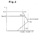
- Fig. 2 is a graph showing the relationship between the current and voltage of the AC adapter 4.
- the AC adapter 4 maintains the DC power supply voltage Vin constant as the supply current I0 increases.
- the overcurrent limiter is activated. This causes the AC adapter 4 to decrease the DC power supply voltage Vin.
- the supply current I0 reaches a maximum limit value I limH (point P2), the AC adapter 4 shifts to a shut-down state. As a result, the DC power supply voltage Vin continues to decrease and the supply current I0 starts to decrease.
- the DC-DC converter 100 which uses the AC adapter 4, maintains the output voltage Vout2, which is lower than the DC power supply voltage vin, constant as the charging current I2 increases.
- the DC-DC converter 100 maintains the charging current I2 constant while decreasing the output voltage Vout2.
- the first to third reference values Vref1-Vref3 are set so that the current supply capacity of the AC adapter 4 can be fully utilized.
- the DC-DC converter 120 has a switch SW which selects a first reference voltage Vref1 from a plurality of reference voltages in accordance with the current supply capacity of the AC adapter. By altering the reference voltage, the supply current I0 of the AC adapter can be optimally adjusted.
- the switch SW is shifted by a control signal from the AC adapter. Accordingly, the AC adapter is required to have a special device. This increases the cost of the AC adapter.
- the switch SW also increases the cost of the DC-DC adapter.
- the present invention provides a method for controlling a DC-DC converter that generates a system output current and a battery charging current from a supply current generated from a DC power supply voltage.
- the method includes the steps of comparing the DC power supply voltage with a reference voltage and generating a differential voltage detection signal from the comparison result, comparing the differential voltage detection signal with a triangular wave signal and generating a duty control signal having a duty ratio corresponding to the comparison result, and controlling the supply current flowing through an output transistor to adjust the battery charging current by activating and deactivating the output transistor in accordance with the duty control signal.
- a circuit for controlling a DC-DC converter that generates a system output current and a battery charging current from a supply current generated from a DC power supply voltage.
- the DC-DC converter includes an output transistor through which the supply current flows.
- the control circuit includes a voltage detection circuit for comparing the DC power supply voltage with a first reference voltage and generating a differential voltage detection signal from the comparison result.
- a PWM comparison circuit is connected to the voltage detection circuit to compare the differential voltage signal with a triangular wave signal and generate a duty control signal having a duty ratio corresponding to the comparison result.
- the PWM comparison circuit provides the duty control signal to the output transistor to activate and deactivate the output transistor, thereby controlling the supply current flowing through the output transistor, and adjusting the battery charging current.
- a DC-DC converter for generating a system output current and a battery charging current from a supply current generated from a DC power supply voltage.
- the DC-DC converter includes a smoothing circuit having an output coil and a capacitor, an output transistor connected to the smoothing circuit, and a control circuit connected to the output transistor to control the supply current flowing through the output transistor.
- the control circuit includes a voltage detection circuit for comparing the DC power supply voltage with a first reference voltage and generating a differential voltage detection signal from the comparison result.
- a PWM comparison circuit is connected to the voltage detection circuit.
- the PWM comparison circuit compares the differential voltage signal with a triangular wave signal and generates a duty control signal having a duty ratio corresponding to the comparison result.
- the PWM comparison circuit provides the duty control signal to the output transistor to activate and deactivate the output transistor, thereby controlling the supply current flowing through the output transistor and adjusting the battery charging current.
- a control circuit for a DC-DC converter is provided.
- the DC-DC converter generates a system output current and a battery charging current from a supply current provided by an AC adapter.
- the DC-DC converter has an output terminal at which the battery charging current is provided, an output transistor connected to the output terminal which supplies the battery charging current, and a coil and a capacitor connected in series between the output transistor and the output terminal.
- the control circuit includes a voltage detection amplifying circuit having a non-inverting input terminal which receives a DC power supply voltage from the AC adapter and an inverting input terminal which receives a first reference voltage.
- the voltage detection amplifying circuit compares the DC power supply voltage and the first reference voltage and amplifies a voltage difference thereof to generate a first detection signal.
- a current detection amplifying circuit has a non-inverting input terminal connected to a first terminal of the resistor and an inverting input terminal connected to a second, opposite terminal of the resistor. The current detection amplifying circuit detects a value of the battery charging current and generates a second detection signal corresponding thereto.
- a first error amplifying circuit has an inverting input terminal connected to an output of the current detection amplifying circuit which receives the second detection signal and a non-inverting input terminal which receives a second reference voltage.
- the first error amplifying circuit compares the second detection signal and the second reference voltage and amplifies a voltage difference thereof to generate a third detection signal.
- a second error amplifying circuit has an inverting input terminal connected to a low potential terminal of the resistor and a non-inverting input terminal which receives a third reference voltage. The second error amplifying circuit compares the potential at the low potential side of the resistor and the third reference voltage and amplifies a voltage difference thereof to generate a fourth detection signal.
- a PWM comparison circuit has a first non-inverting input terminal connected to the voltage detection amplifying circuit and receiving the first detection signal, a second non-inverting input terminal connected to the first error amplifying circuit and receiving the third detection signal, a third non-inverting input terminal connected to the second error amplifying circuit and receiving the fourth detection signal, and an inverting input terminal which receives a triangular wave signal.
- the PWM comparison circuit compares one of the first, third and fourth detection signals with the triangular wave signal and amplifies a voltage difference thereof to generate a duty control signal.
- An output circuit is connected between the output transistor and the PWM comparison circuit for activating and deactivating the transistor in accordance with the duty control signal in order to adjust the battery charging current.
- a method for controlling a DC-DC converter in another aspect of the present invention, includes the steps of detecting the DC power supply voltage and adjusting the battery charging current in accordance with the detected DC power supply voltage.
- a circuit for controlling a DC-DC converter is provided.
- the DC-DC converter generates an output current and a battery charging current from a supply current generated from a DC power supply voltage.
- the DC-DC converter includes an output switch through which the supply current flows to output the charging current.
- the control circuit includes a voltage detection circuit for detecting the DC power supply voltage; and an adjusting circuit connected to the voltage detection circuit for adjusting the battery charging current in accordance with the detected DC power supply voltage.
- a DC-DC converter for generating a system output current and a battery charging current from a supply current generated from a DC power supply voltage.
- the DC-DC converter includes a smoothing circuit including an output coil and a capacitor, an output switch connected to the smoothing circuit, and a control circuit connected to the output switch to control the supply current flowing through the output switch.
- the control circuit includes a voltage detection circuit for detecting the DC power supply voltage and an adjusting circuit connected to the voltage detection circuit for adjusting the battery charging current in accordance with the detected DC power supply voltage.
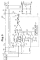
- Fig. 4 is a circuit diagram showing a DC-DC converter 20 according to a first embodiment of the present invention.
- the DC-DC converter 20 has a control circuit 21, which includes a current detection amplifying circuit 12, a voltage detection amplifying circuit 22, a first error amplifying circuit 14, a second error amplifying circuit 15, a PWM comparison circuit 16 as an adjusting circuit, a triangular wave oscillating circuit 17, and an output circuit 18.
- the voltage detection amplifying circuit 22 has a non-inverting input terminal, which receives the DC power supply voltage Vin from the AC adapter 4, and an inverting input terminal, which receives a first reference voltage Vref1.
- the voltage detection amplifying circuit 22 compares the DC power supply voltage Vin with the first reference voltage Vrefl and amplifies the voltage difference to generate a detection signal SG9, which is provided to a first non-inverting input terminal of the PWM comparison circuit 16. In this case, a decrease in the DC power supply voltage Vin decreases the potential of the detection signal SG9, and an increase in the DC power supply voltage Vin increases the potential of the detection signal SG9.
- the PWM comparison circuit 16 selects the signal having the lowest level and compares the selected signal with a triangular wave signal SG7 provided to the inverting input terminal.
- the PWM comparison circuit 16 outputs a pulse signal having a low level when the triangular wave signal SG7 is greater than the detection signal or the error output signals and outputs a pulse signal having a high level when the triangular wave signal SG7 is smaller than the detection signal or the error output signals.
- the pulse signal, or duty control signal SG8 is received by the output circuit 18.
- the output circuit 18 inverts the control signal SG8 and sends an output signal SG1 to the gate of an output transistor 3.
- the PWM comparison circuit 16 compares the first error output signal SG5 with the triangular wave signal SG7 and generates a duty control signal SG8 having a duty ratio corresponding to the comparison result.
- the duty control signal SG8 is inverted by the output circuit 18 and applied to the output transistor 3 as the output signal SG1.
- the output transistor 3 is activated and deactivated in response to the output signal SG1 to converge the charging current I2 of the battery BT on the predetermined value
- the PWM comparison circuit 16 compares the second error output signal SG6 with the triangular wave signal SG7 and generates a duty control signal SG8 having a duty ratio corresponding to the comparison result.
- the duty control signal SG8 is inverted by the output circuit 18 and applied to the output transistor 3 as the output signal SG1.
- the output transistor 3 is activated and deactivated in response to the output signal SG1 to converge the output voltage Vout2 of the battery BT on the predetermined value.
- the DC power supply voltage Vin of the AC adapter 4 decreases. If the detection signal SG9 is smaller than the first and second error output signals SG5, SG6, the PWM comparison circuit 16 compares the detection signal SG9 with the triangular wave signal SG7. The decrease in the potential of the detection signal SG9 prolongs the period during which the potential of the triangular wave signal SG7 exceeds the potential of the detection signal SG9.
- the duty control signal SG8 output from the PWM comparison circuit 16 remains high for a short period (i.e., has a low duty ratio).
- the output circuit 18 inverts the duty control signal SG8 and provides the output transistor 3 with an output signal SG1 having an increased duty ratio. This shortens the period during which the output transistor 3 is activated and decreases the charging current I2. As a result, the DC power supply voltage Vin increases and the output voltage Vout2 of the battery BT decreases.
- An increase in the DC power supply voltage Vin increases the potential of the detection signal SG9 output by the voltage detection amplifying circuit 22.
- the increase in the potential of the detection signal SG9 shortens the period during which the potential of the triangular wave signal SG3 exceeds the potential of the detection signal SG9.
- the period during which the triangular wave signal SG3 is equal to or lower than the detection signal SG9 is prolonged.
- the duty control signal SG8 output from the PWM comparison circuit 16 remains high for a long period (i.e., has a high duty ratio).
- the output circuit 18 inverts the duty control signal SG8 and provides the output transistor 3 with an output signal SG1 having a decreased duty ratio.
- the DC-DC converter 20 of the first embodiment has the advantages described below.
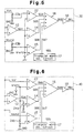
- Fig. 5 is a circuit diagram showing a control circuit 30 of a DC-DC converter according to a second embodiment of the present invention.
- the second reference voltage Vref2 is set so that it is lower than the first and third reference voltages Vref1, Vref3.
- the second reference voltage Vref2 is provided to the inverting input terminal of a voltage detection amplifying circuit 22 and the non-inverting input terminals of first and second error amplifying circuits 14, 15.
- the control circuit 30 includes a resistance voltage dividing circuit 23a connected to the non-inverting input terminal of the voltage detection amplifying circuit 22 and a resistance voltage dividing circuit 23b connected to the inverting input terminal of the second error amplifying circuit 15.
- the resistance voltage dividing circuit 23a is configured to decrease the DC power supply voltage Vin in accordance with the second reference voltage Vref2.
- the resistance voltage dividing circuit 23b is configured to decrease the output voltage Vout2 in accordance with the second reference voltage Vref2.
- the resistance voltage dividing circuits 23a, 23b divide the DC power supply voltage Vin and the output voltage Vout2, respectively.
- a single power supply is enough to generate the single reference voltage Vref2.
- the second embodiment may be modified by providing the first reference voltage Vref1 to the voltage detection amplifying circuit 22 and the first and second error amplifying circuits 14, 15.
- the resistor voltage dividing circuit 23a is replaced by a resistor voltage dividing circuit, which divides the voltage of the voltage signal SG4. This resistor voltage dividing circuit is connected between the current detection amplifying circuit 12 and the first error amplifying circuit 14.
- Fig. 6 is a circuit diagram showing a control circuit 40 of a DC-DC converter according to a third embodiment of the present invention.
- the first reference voltage Vref1 is set so that it is higher than the second and third reference voltages Vref2, Vref3.
- the first reference voltage Vref1 is provided to the inverting input terminal of the voltage detection amplifying circuit 22.
- the control circuit 40 includes a resistance voltage dividing circuit 24a connected between the first reference voltage Vref1 and the non-inverting input terminal of the first error amplifying circuit 14, and a resistance voltage dividing circuit 24b connected between the first reference voltage Vref1 and the non-inverting input terminal of the second error amplifying circuit 15.
- the resistance voltage dividing circuit 24a decreases the first reference voltage Vref1 and generates the second reference voltage Vref2, which is provided to the first error amplifying circuit 14.
- the resistance voltage dividing circuit 24b decreases the first reference voltage Vref1 and generates the third reference voltage Vref3, which is provided to the second error amplifying circuit 15.
- the resistance voltage dividing circuits 24a, 24b divide the first reference voltage Vref to generate the second and third reference voltages Vref.
- only a single power supply is required to generate the single reference voltage Vref1.
- the third embodiment may be modified by directly providing the second reference voltage Vref2 to the first error amplifying circuit 14.
- a resistance voltage dividing circuit which divides the second reference voltage Vref2 and generates the first reference voltage Vref1
- a resistance voltage dividing circuit which divides the second reference voltage Vref2 and generates the third reference voltage Vref3, are provided.
- An n-channel MOS transistor may be employed as the output transistor 3.
- the output circuit 18 includes an buffer circuit or an even number of inverters, which are connected in series to one another.
- the triangular wave oscillating circuit 17 may be formed on a semiconductor integrated circuit chip that differs from the semiconductor integrated circuit chip on which the control circuit 21 is formed.
- the control circuit 21 may be formed on the same semiconductor integrated circuit chip as the output transistor 3 and a smoothing circuit that includes the output coil 4 and the capacitor 7. That is, the DC-DC converter may be formed on a single semiconductor substrate.
Landscapes
- Engineering & Computer Science (AREA)
- Power Engineering (AREA)
- Theoretical Computer Science (AREA)
- Physics & Mathematics (AREA)
- General Engineering & Computer Science (AREA)
- General Physics & Mathematics (AREA)
- Dc-Dc Converters (AREA)
- Charge And Discharge Circuits For Batteries Or The Like (AREA)
Abstract
Description
Claims (21)
- A method for controlling a DC-DC converter that generates a system output current and a battery charging current from a supply current generated from a DC power supply voltage, the method comprising the steps of:comparing the DC power supply voltage with a reference voltage and generating a differential voltage detection signal from the comparison result;comparing the differential voltage detection signal with a triangular wave signal and generating a duty control signal having a duty ratio corresponding to the comparison result; andcontrolling the supply current flowing through an output transistor to adjust the battery charging current by activating and deactivating the output transistor in accordance with the duty control signal.
- The DC-DC converter controlling method according to claim 1, further comprising the steps of:detecting the battery charging current; andcontrolling the battery charging current so that it remains substantially constant using the detected battery charging current.
- The DC-DC converter controlling method according to claim 1, further comprising the steps of:detecting a battery charging voltage based on the battery charging current; andcontrolling the battery charging voltage so that it remains substantially constant using the detected battery charging voltage.
- A circuit for controlling a DC-DC converter that generates a system output current and a battery charging current from a supply current generated from a DC power supply voltage, wherein the DC-DC converter includes an output transistor (3) through which the supply current flows, wherein the control circuit comprises:a voltage detection circuit (22) for comparing the DC power supply voltage with a first reference voltage and generating a differential voltage detection signal from the comparison result; anda PWM comparison circuit (16) connected to the voltage detection circuit for comparing the differential voltage detection signal with a triangular wave signal and generating a duty control signal having a duty ratio corresponding to the comparison result, the PWM comparison circuit providing the duty control signal to the output transistor to activate and deactivate the output transistor, thereby controlling the supply current flowing through the output transistor, and adjusting the battery charging current.
- The DC-DC converter control circuit according to claim 4, further comprising a charging current detection circuit (12, 14) for detecting the battery charging current and generating a charging current detection signal, wherein the PWM comparison circuit compares the charging current detection signal with the triangular wave signal and generates the duty control signal having a duty ratio corresponding to the comparison result, the PWM comparison circuit providing the duty control signal to the output transistor to activate and deactivate the output transistor, thereby controlling the supply current flowing through the output transistor, and maintain the battery charging current constant.
- The DC-DC converter control circuit according to claim 5, wherein the charging current detection circuit includes:a current detection circuit (12) for converting the battery charging current to a voltage signal; andan error amplifying circuit (14) connected to the current detection circuit to compare the voltage signal with a second reference voltage and generate the charging current detection signal.
- The DC-DC converter control circuit according to any one of claims 4 to 6, wherein the voltage detection circuit (22) receives the second reference voltage as the first reference voltage, and the control circuit further comprises:
a resistance dividing circuit (23a) connected to the voltage detection circuit to divide the DC power supply voltage in accordance with the second reference voltage and provide the divided voltage to the voltage detection circuit. - The DC-DC converter control circuit according to claim 6, further comprising a resistance dividing circuit (24a) connected to the error amplifying circuit to divide the first reference voltage, generate the second reference voltage, and provide the second reference voltage to the error amplifying circuit.
- The DC-DC converter control circuit according to claim 6, wherein the error amplifying circuit receives the first reference voltage as the second reference voltage, and wherein the control circuit further comprises a resistance dividing circuit for dividing the voltage of the voltage signal from the current detection circuit in accordance with the first reference voltage and providing the divided voltage to the error amplifying circuit.
- The DC-DC converter control circuit according to any one of claims 4 to 6, further comprising a resistance dividing circuit connected to the voltage detection circuit to divide the second reference voltage, generate the first reference voltage, and provide the first reference voltage to the voltage detection circuit.
- The DC-DC converter control circuit according to claim 4, further comprising a charging voltage detection circuit (15) for detecting a battery charging voltage based on the battery charging current and generating a charging voltage detection signal, wherein the PWM comparison circuit compares the charging voltage detection signal with the triangular wave signal and generates the duty control signal having a duty ratio corresponding to the comparison result, the PWM comparison circuit providing the duty control signal to the output transistor to activate and deactivate the output transistor to control the supply current flowing through the output transistor, and maintain the battery charging voltage constant.
- The DC-DC converter control circuit according to claim 11, wherein the charging voltage detection circuit includes an error amplifying circuit (15) for comparing the battery charging voltage with a second reference voltage to generate a charging voltage detection signal.
- The DC-DC converter control circuit according to claim 12, wherein the error amplifying circuit (15) receives the first reference voltage as the second reference voltage, the control circuit further comprising a resistance dividing circuit (24a) for dividing the battery charging voltage in accordance with the first reference voltage and providing the divided voltage to the error amplifying circuit.
- The DC-DC converter control circuit according to claim 12, further comprising a resistance dividing circuit (24b) connected to the error amplifying circuit to divide the first reference voltage, generate the second reference voltage, and provide the second reference voltage to the error amplifying circuit.
- The DC-DC converter control circuit according to any one of claims 4, 11 and 12, wherein the voltage detection circuit (22) receives the second reference voltage as the first reference voltage, the control circuit further comprising a resistance dividing circuit connected to the voltage detection circuit to divide the DC power supply voltage in accordance with the second reference voltage and provide the divided voltage to the voltage detection circuit.
- The DC-DC converter control circuit according to any one of claims 4, 11 and 12, further comprising a resistance dividing circuit connected to the voltage detection circuit to divide the second reference voltage, generate the first reference voltage, and provide the first reference voltage to the voltage detection circuit.
- A DC-DC converter for generating a system output current and a battery charging current from a supply current generated from a DC power supply voltage, the DC-DC converter comprising:a smoothing circuit including an output coil (5) and a capacitor (7);an output transistor (3) connected to the smoothing circuit; anda control circuit (21) connected to the output transistor to control the supply current flowing through the output transistor, wherein the control circuit includes:a voltage detection circuit (22) for comparing the DC power supply voltage with a first reference voltage and generating a differential voltage detection signal from the comparison result; anda PWM comparison circuit (16) connected to the voltage detection circuit, wherein the PWM comparison circuit compares the differential voltage signal with a triangular wave signal and generates a duty control signal having a duty ratio corresponding to the comparison result, the PWM comparison circuit providing the duty control signal to the output transistor to activate and deactivate the output transistor, thereby controlling the supply current flowing through the output transistor and adjusting the battery charging current.
- A control circuit for a DC-DC converter, the DC-DC converter generating a system output current and a battery charging current from a supply current provided by an AC adapter (4), wherein the DC-DC converter has an output terminal (EX1) at which the battery charging current is provided, an output transistor (3) connected to the-output terminal which supplies the battery charging current, and a coil (5) and a capacitor (7) connected in series between the output transistor and the output terminal, the control circuit comprising:a voltage detection amplifying circuit (22) having a non-inverting input terminal which receives a DC power supply voltage from the AC adapter and an inverting input terminal which receives a first reference voltage, the voltage detection amplifying circuit comparing the DC power supply voltage and the first reference voltage and amplifying a voltage difference thereof to generate a first detection signal;a current detection amplifying circuit (12) having a non-inverting input terminal connected to a first terminal of the resistor and an inverting input terminal connected to a second, opposite terminal of the resistor, the current detection amplifying circuit detecting a value of the battery charging current and generating a second detection signal corresponding thereto;a first error amplifying circuit (14) having an inverting input terminal connected to an output of the current detection amplifying circuit which receives the second detection signal and a non-inverting input terminal which receives a second reference voltage, the first error amplifying circuit comparing the second detection signal and the second reference voltage and amplifying a voltage difference thereof to generate a third detection signal;a second error amplifying circuit (15) having an inverting input terminal connected to a low potential terminal of the resistor and a non-inverting input terminal which receives a third reference voltage, the second error amplifying circuit comparing the potential at the low potential side of the resistor and the third reference voltage and amplifying a voltage difference thereof to generate a fourth detection signal;a PWM comparison circuit (16) having a first non-inverting input terminal connected to the voltage detection amplifying circuit and receiving the first detection signal, a second non-inverting input terminal connected to the first error amplifying circuit and receiving the third detection signal, a third non-inverting input terminal connected to the second error amplifying circuit and receiving the fourth detection signal, and an inverting input terminal which receives a triangular wave signal, the PWM comparison circuit comparing one of the first, third and fourth detection signals with the triangular wave signal and amplifying a voltage difference thereof to generate a duty control signal; andan output circuit (18) connected between the output transistor and the PWM comparison circuit for activating and deactivating the transistor in accordance with the duty control signal in order to adjust the battery charging current.
- A method for controlling a DC-DC converter that generates a system output current and a battery charging current from a supply current generated from a DC power supply voltage, the method comprising the steps of;detecting the DC power supply voltage;adjusting the battery charging current in accordance with the detected DC power supply voltage.
- A circuit for controlling a DC-DC converter that generates an output current and a battery charging current from a supply current generated from a DC power supply voltage, wherein the DC-DC converter includes an output switch (3) through which the supply current flows to output the charging current, wherein the control circuit comprises:a voltage detection circuit (22) for detecting the DC power supply voltage; andan adjusting circuit (16) connected to the voltage detection circuit for adjusting the battery charging current in accordance with the detected DC power supply voltage.
- A DC-DC converter for generating a system output current and a battery charging current from a supply current generated from a DC power supply voltage, the DC-DC converter comprising:a smoothing circuit including an output coil (5) and a capacitor (7);an output switch (3) connected to the smoothing circuit; anda control circuit connected to the output switch to control the supply current flowing through the output switch, wherein the control circuit includes:a voltage detection circuit (22) for detecting the DC power supply voltage; andan adjusting circuit (16) connected to the voltage detection circuit for adjusting the battery charging current in accordance with the detected DC power supply voltage.
Applications Claiming Priority (2)
| Application Number | Priority Date | Filing Date | Title |
|---|---|---|---|
| JP28658698 | 1998-10-08 | ||
| JP28658698 | 1998-10-08 |
Publications (3)
| Publication Number | Publication Date |
|---|---|
| EP0993103A2 true EP0993103A2 (en) | 2000-04-12 |
| EP0993103A3 EP0993103A3 (en) | 2000-05-10 |
| EP0993103B1 EP0993103B1 (en) | 2005-12-28 |
Family
ID=17706346
Family Applications (1)
| Application Number | Title | Priority Date | Filing Date |
|---|---|---|---|
| EP99307922A Expired - Lifetime EP0993103B1 (en) | 1998-10-08 | 1999-10-07 | Controller for DC-DC converter |
Country Status (6)
| Country | Link |
|---|---|
| US (1) | US6194875B1 (en) |
| EP (1) | EP0993103B1 (en) |
| KR (1) | KR20000028826A (en) |
| CN (1) | CN1145092C (en) |
| DE (1) | DE69929132T2 (en) |
| TW (1) | TW448350B (en) |
Cited By (3)
| Publication number | Priority date | Publication date | Assignee | Title |
|---|---|---|---|---|
| EP1227563A2 (en) | 2000-12-29 | 2002-07-31 | Nokia Corporation | Method for charging a battery |
| RU2337393C1 (en) * | 2007-07-02 | 2008-10-27 | Открытое акционерное общество "Научно-производственный центр "Полюс" | Method of even current distribution control in multi-chanel pulse voltage transducer |
| RU2339993C1 (en) * | 2007-07-02 | 2008-11-27 | Открытое акционерное общество "Научно-производственный центр "Полюс" | Method of reversible pulse dc voltage converter control with stabilisation of limit current |
Families Citing this family (36)
| Publication number | Priority date | Publication date | Assignee | Title |
|---|---|---|---|---|
| US6693413B1 (en) * | 1994-04-26 | 2004-02-17 | Comarco Wireless Technologies, Inc. | Programmable power supply |
| US7145787B2 (en) | 1994-04-26 | 2006-12-05 | Comarco Wireless Technologies, Inc. | Programmable power supply |
| US6281662B1 (en) * | 2000-10-18 | 2001-08-28 | Ford Global Technologies, Inc. | Battery charging DC to DC converter |
| WO2002089286A1 (en) * | 2001-04-30 | 2002-11-07 | Infineon Technologies Ag | Dc-dc conversion charging apparatus |
| US6674180B2 (en) | 2001-10-12 | 2004-01-06 | Ford Global Technologies, Llc | Power supply for a hybrid electric vehicle |
| JP3904489B2 (en) * | 2002-07-04 | 2007-04-11 | 富士通株式会社 | Charge control circuit, charger, power supply circuit, information processing apparatus, and battery pack |
| JP3944605B2 (en) * | 2002-09-30 | 2007-07-11 | ローム株式会社 | Switching power supply |
| US6836101B2 (en) * | 2002-12-05 | 2004-12-28 | Comarco Wireless Technologies, Inc. | Tip having active circuitry |
| US6844705B2 (en) * | 2002-12-09 | 2005-01-18 | Intersil Americas Inc. | Li-ion/Li-polymer battery charger configured to be DC-powered from multiple types of wall adapters |
| CN100375942C (en) * | 2003-09-26 | 2008-03-19 | 纬创资通股份有限公司 | System device with identifiable power adapter and identification method |
| TWI312223B (en) * | 2003-11-14 | 2009-07-11 | Beyond Innovation Tech Co Ltd | A pulse width modulation control circuit and the loading system of its application |
| US9153960B2 (en) | 2004-01-15 | 2015-10-06 | Comarco Wireless Technologies, Inc. | Power supply equipment utilizing interchangeable tips to provide power and a data signal to electronic devices |
| US20080024099A1 (en) * | 2004-03-15 | 2008-01-31 | Rohm Co., Ltd. | Power Supply Apparatus |
| CN100463400C (en) * | 2006-02-11 | 2009-02-18 | 鸿富锦精密工业(深圳)有限公司 | Digital subscriber loop terminal and its power supply system |
| JP4789662B2 (en) * | 2006-03-17 | 2011-10-12 | 富士通セミコンダクター株式会社 | Power supply device control circuit, power supply device and control method therefor |
| JP4837408B2 (en) | 2006-03-20 | 2011-12-14 | 富士通セミコンダクター株式会社 | DC-DC converter, control circuit for DC-DC converter, and control method for DC-DC converter |
| JP4668836B2 (en) * | 2006-05-09 | 2011-04-13 | ローム株式会社 | CHARGE CONTROL CIRCUIT AND CHARGE CIRCUIT AND ELECTRONIC DEVICE USING THE SAME |
| US7759905B2 (en) * | 2006-09-01 | 2010-07-20 | Via Technologies, Inc. | Linear battery charger |
| US7656132B2 (en) * | 2006-11-14 | 2010-02-02 | Advanced Analogic Technologies, Inc. | Battery charger apparatus with a digital charge reduction loop |
| JP4755153B2 (en) * | 2007-08-23 | 2011-08-24 | 株式会社リコー | Charging circuit |
| CN101884153A (en) * | 2007-12-03 | 2010-11-10 | 罗姆股份有限公司 | power management circuit |
| US8159204B2 (en) * | 2008-09-29 | 2012-04-17 | Active-Semi, Inc. | Regulating current output from a buck converter without external current sensing |
| US20100164437A1 (en) * | 2008-10-24 | 2010-07-01 | Mckinley Joseph P | Battery formation and charging system and method |
| US8213204B2 (en) * | 2009-04-01 | 2012-07-03 | Comarco Wireless Technologies, Inc. | Modular power adapter |
| US8354760B2 (en) * | 2009-10-28 | 2013-01-15 | Comarco Wireless Technologies, Inc. | Power supply equipment to simultaneously power multiple electronic device |
| JP2011199993A (en) * | 2010-03-18 | 2011-10-06 | Rohm Co Ltd | Charge controller, load driver |
| JP5682423B2 (en) * | 2011-04-04 | 2015-03-11 | ミツミ電機株式会社 | Battery protection circuit, battery protection device, and battery pack |
| US9088209B2 (en) * | 2011-05-17 | 2015-07-21 | Eaton Corporation | Parasitic power supply and sensor apparatus including a power supply |
| CN102412712A (en) * | 2011-11-29 | 2012-04-11 | 杭州矽力杰半导体技术有限公司 | Compensation control circuit and method for direct current converter |
| US20130147277A1 (en) * | 2011-12-08 | 2013-06-13 | O2Micro Inc. | Power management system |
| CN104335469B (en) * | 2012-06-08 | 2017-06-13 | 瑞典爱立信有限公司 | Controlling switch mode power is come with maximum power efficiency |
| WO2014049945A1 (en) * | 2012-09-27 | 2014-04-03 | 旭化成エレクトロニクス株式会社 | Switching power supply circuit |
| US9793796B2 (en) * | 2015-02-23 | 2017-10-17 | Infineon Technologies Austria Ag | Driver controller with AC-adapted and DC-adapted control modes |
| US9837844B2 (en) * | 2016-03-08 | 2017-12-05 | Nxp Usa, Inc. | Regulation circuit having analog and digital feedback and method therefor |
| KR20230078214A (en) * | 2021-11-26 | 2023-06-02 | 현대자동차주식회사 | Apparatus and Method for converting multi-output power |
| CN116679815B (en) * | 2023-07-28 | 2023-10-27 | 长城电源技术有限公司 | Server power supply and control method thereof |
Family Cites Families (12)
| Publication number | Priority date | Publication date | Assignee | Title |
|---|---|---|---|---|
| ES2048806T3 (en) * | 1989-09-29 | 1994-04-01 | Siemens Ag | CIRCUIT PROVISION FOR A REGULATED LOCKING CONVERTER CONNECTION POWER SUPPLY. |
| US5490055A (en) * | 1993-03-03 | 1996-02-06 | At&T Corp. | Multiloop feedback control apparatus for DC/DC converters with frequency-shaping band pass current control |
| JP3129364B2 (en) | 1993-06-23 | 2001-01-29 | サンケン電気株式会社 | DC-DC converter |
| IT1268472B1 (en) | 1993-10-22 | 1997-03-04 | St Microelectronics Srl | BUCK CONVERTER WITH OPERATING MODE AUTOMATICALLY DETERMINED BY THE LOAD LEVEL |
| JPH07322602A (en) | 1994-05-23 | 1995-12-08 | Fujitsu Ltd | Power supply |
| US5484166A (en) * | 1994-07-22 | 1996-01-16 | Trw Vehicle Safety Systems Inc. | Method and apparatus for providing a deployment signal for a vehicle occupant restraint device during a side impact crash |
| KR970010485B1 (en) * | 1994-08-25 | 1997-06-26 | 엘지전자 주식회사 | Multiple Output Circuit of Projective Lamp |
| JP3069498B2 (en) * | 1994-09-01 | 2000-07-24 | 富士通株式会社 | Charge / discharge device and electronic equipment |
| JPH09172772A (en) | 1995-12-20 | 1997-06-30 | Fujitsu Denso Ltd | Power supply apparatus having drooping characteristics of output voltage |
| JP3920371B2 (en) * | 1996-01-29 | 2007-05-30 | 富士通株式会社 | Charging device, current detection circuit, and voltage detection circuit |
| US5966003A (en) * | 1997-05-15 | 1999-10-12 | Fujitsu Limited | DC-DC converter control circuit |
| JP2000069746A (en) * | 1998-08-21 | 2000-03-03 | Fujitsu Ltd | Control method of DC-DC converter, control circuit of DC-DC converter, and DC-DC converter |
-
1999
- 1999-10-05 KR KR1019990042735A patent/KR20000028826A/en not_active Ceased
- 1999-10-07 EP EP99307922A patent/EP0993103B1/en not_active Expired - Lifetime
- 1999-10-07 US US09/414,432 patent/US6194875B1/en not_active Expired - Fee Related
- 1999-10-07 DE DE69929132T patent/DE69929132T2/en not_active Expired - Fee Related
- 1999-10-08 TW TW088117388A patent/TW448350B/en not_active IP Right Cessation
- 1999-10-08 CN CNB991208846A patent/CN1145092C/en not_active Expired - Fee Related
Cited By (4)
| Publication number | Priority date | Publication date | Assignee | Title |
|---|---|---|---|---|
| EP1227563A2 (en) | 2000-12-29 | 2002-07-31 | Nokia Corporation | Method for charging a battery |
| EP1227563A3 (en) * | 2000-12-29 | 2003-11-05 | Nokia Corporation | Method for charging a battery |
| RU2337393C1 (en) * | 2007-07-02 | 2008-10-27 | Открытое акционерное общество "Научно-производственный центр "Полюс" | Method of even current distribution control in multi-chanel pulse voltage transducer |
| RU2339993C1 (en) * | 2007-07-02 | 2008-11-27 | Открытое акционерное общество "Научно-производственный центр "Полюс" | Method of reversible pulse dc voltage converter control with stabilisation of limit current |
Also Published As
| Publication number | Publication date |
|---|---|
| DE69929132T2 (en) | 2006-06-29 |
| KR20000028826A (en) | 2000-05-25 |
| EP0993103B1 (en) | 2005-12-28 |
| TW448350B (en) | 2001-08-01 |
| DE69929132D1 (en) | 2006-02-02 |
| CN1250898A (en) | 2000-04-19 |
| US6194875B1 (en) | 2001-02-27 |
| CN1145092C (en) | 2004-04-07 |
| EP0993103A3 (en) | 2000-05-10 |
Similar Documents
| Publication | Publication Date | Title |
|---|---|---|
| EP0993103B1 (en) | Controller for DC-DC converter | |
| JP4647747B2 (en) | DC-DC converter and semiconductor integrated circuit device for DC-DC converter | |
| US7315153B2 (en) | Switching power supply in an integrated circuit having a comparator with two threshold values, a synchronization input and output, voltage feedback and efficient current sensing | |
| US7122995B2 (en) | Multi-phase DC-DC converter and control circuit for multi-phase DC-DC converter | |
| JP4671275B2 (en) | Power supply control device, power supply electronic component and power supply device | |
| US6611132B2 (en) | DC-DC converter, power supply circuit, method for controlling DC-DC converter, and method for controlling power supply circuit | |
| US8018694B1 (en) | Over-current protection for a power converter | |
| US9887626B2 (en) | Adaptive feedback control system and method for voltage regulators | |
| JP4686579B2 (en) | Power supply | |
| US7781909B2 (en) | Control circuit of power supply, power supply and control method thereof | |
| EP2136462A1 (en) | DC-DC Converter | |
| KR100718522B1 (en) | Dc-dc converter, circuit for controlling dc-dc converter, and method for controlling dc-dc converter | |
| JP7577582B2 (en) | Step-down DC/DC converter, controller therefor, control method therefor, and electronic device | |
| KR20080039874A (en) | Step-down switching regulators and control circuits thereof and electronic devices using them | |
| JP2012060714A (en) | Integrated circuit | |
| CN102377336A (en) | Switching power source apparatus | |
| KR20110045099A (en) | DC-DC converter | |
| JP3691635B2 (en) | Voltage control circuit and DC / DC converter | |
| US20250070645A1 (en) | Gate drive circuit, power good circuit, overcurrent detection circuit, oscillation prevention circuit, switching control circuit and switching power supply device | |
| JP2019017210A (en) | Drive circuit of high-side transistor, control circuit of dc/dc converter arranged by use thereof, and dc/dc converter | |
| US20080150505A1 (en) | Switching regulator and semiconductor device having the same | |
| US8044641B2 (en) | Step-down switching regulator with turn off undershoot prevention | |
| US9871456B2 (en) | Voltage conversion device and method of operation | |
| US7009369B2 (en) | Advanced monitoring algorithm for regulated power systems with single output flag | |
| US6987378B1 (en) | Over-voltage protection circuit and method therefor |
Legal Events
| Date | Code | Title | Description |
|---|---|---|---|
| PUAI | Public reference made under article 153(3) epc to a published international application that has entered the european phase |
Free format text: ORIGINAL CODE: 0009012 |
|
| PUAL | Search report despatched |
Free format text: ORIGINAL CODE: 0009013 |
|
| AK | Designated contracting states |
Kind code of ref document: A2 Designated state(s): DE FR GB |
|
| AX | Request for extension of the european patent |
Free format text: AL;LT;LV;MK;RO;SI |
|
| AK | Designated contracting states |
Kind code of ref document: A3 Designated state(s): AT BE CH CY DE DK ES FI FR GB GR IE IT LI LU MC NL PT SE |
|
| AX | Request for extension of the european patent |
Free format text: AL;LT;LV;MK;RO;SI |
|
| 17P | Request for examination filed |
Effective date: 20000925 |
|
| AKX | Designation fees paid |
Free format text: DE FR GB |
|
| 17Q | First examination report despatched |
Effective date: 20050117 |
|
| GRAP | Despatch of communication of intention to grant a patent |
Free format text: ORIGINAL CODE: EPIDOSNIGR1 |
|
| GRAS | Grant fee paid |
Free format text: ORIGINAL CODE: EPIDOSNIGR3 |
|
| RIN1 | Information on inventor provided before grant (corrected) |
Inventor name: KITAGAWA, SEIYA C/O FUJITSU LIMITED, Inventor name: OZAWA, HIDEKIYO C/O FUJITSU LIMITED Inventor name: MATSUYAMA, TOSHIYUKI,C/O FUJITSU VLSI LIMITED Inventor name: TAKIMOTO, KYUICHI,C/O FUJITSU VLSI LIMITED |
|
| GRAA | (expected) grant |
Free format text: ORIGINAL CODE: 0009210 |
|
| AK | Designated contracting states |
Kind code of ref document: B1 Designated state(s): DE FR GB |
|
| REG | Reference to a national code |
Ref country code: GB Ref legal event code: FG4D |
|
| REF | Corresponds to: |
Ref document number: 69929132 Country of ref document: DE Date of ref document: 20060202 Kind code of ref document: P |
|
| PLBE | No opposition filed within time limit |
Free format text: ORIGINAL CODE: 0009261 |
|
| STAA | Information on the status of an ep patent application or granted ep patent |
Free format text: STATUS: NO OPPOSITION FILED WITHIN TIME LIMIT |
|
| 26N | No opposition filed |
Effective date: 20060929 |
|
| PG25 | Lapsed in a contracting state [announced via postgrant information from national office to epo] |
Ref country code: DE Free format text: LAPSE BECAUSE OF NON-PAYMENT OF DUE FEES Effective date: 20070501 |
|
| GBPC | Gb: european patent ceased through non-payment of renewal fee |
Effective date: 20061007 |
|
| PG25 | Lapsed in a contracting state [announced via postgrant information from national office to epo] |
Ref country code: GB Free format text: LAPSE BECAUSE OF NON-PAYMENT OF DUE FEES Effective date: 20061007 |
|
| PG25 | Lapsed in a contracting state [announced via postgrant information from national office to epo] |
Ref country code: FR Free format text: LAPSE BECAUSE OF FAILURE TO SUBMIT A TRANSLATION OF THE DESCRIPTION OR TO PAY THE FEE WITHIN THE PRESCRIBED TIME-LIMIT Effective date: 20070216 |
|
| PG25 | Lapsed in a contracting state [announced via postgrant information from national office to epo] |
Ref country code: FR Free format text: LAPSE BECAUSE OF FAILURE TO SUBMIT A TRANSLATION OF THE DESCRIPTION OR TO PAY THE FEE WITHIN THE PRESCRIBED TIME-LIMIT Effective date: 20051228 |