EP0992931B1 - Microwave tagging system - Google Patents
Microwave tagging system Download PDFInfo
- Publication number
- EP0992931B1 EP0992931B1 EP98118821A EP98118821A EP0992931B1 EP 0992931 B1 EP0992931 B1 EP 0992931B1 EP 98118821 A EP98118821 A EP 98118821A EP 98118821 A EP98118821 A EP 98118821A EP 0992931 B1 EP0992931 B1 EP 0992931B1
- Authority
- EP
- European Patent Office
- Prior art keywords
- circular
- polarized
- sub
- main unit
- unit
- Prior art date
- Legal status (The legal status is an assumption and is not a legal conclusion. Google has not performed a legal analysis and makes no representation as to the accuracy of the status listed.)
- Expired - Lifetime
Links
Images


Classifications
-
- G—PHYSICS
- G06—COMPUTING; CALCULATING OR COUNTING
- G06K—GRAPHICAL DATA READING; PRESENTATION OF DATA; RECORD CARRIERS; HANDLING RECORD CARRIERS
- G06K7/00—Methods or arrangements for sensing record carriers, e.g. for reading patterns
- G06K7/0008—General problems related to the reading of electronic memory record carriers, independent of its reading method, e.g. power transfer
Definitions
- the invention refers to the field of radio communication for tagging systems.
- the invention is based on the subject-matter as set forth in the preamble of the claims 1 and 13.
- Radio-frequency identification (RFID) systems serve mainly to manage production lines and manufacturing processes of various kinds of products in a highly efficient way.
- Data carriers or tags are attached to work pieces transported on a conveyor belt, to a carrying plate such as a pallet or to containers on a railway carriage.
- the memory of the data carrier contains an identification code of the object the data carrier is attached to, data processing instructions and the like.
- a number of main apparatuses are arranged along the conveyor belt to conduct communication with the passing data carriers by writing data in or reading data from their memories. After updating the memory of a data carrier, the work piece is transferred to the next production process.
- Microwave tagging systems of the described kind are battery-powered and thus must have a low power consumption at simultaneously low demodulation error rate. These two requirements are often in conflict because modulation schemes with low error rates need power-demanding demodulation circuits.
- Typical application areas of such microwave tagging systems are manufacturing halls with metallic walls reflecting incident microwaves and hence causing demodulation errors due to multipath propagation, circular polarization inversions and signal fading effects. Therefore a need for safe data transmission in terms of few demodulation errors in combination with low power consumption and small tag dimensions exists.
- an RFID system using tags attached to moving articles is disclosed.
- the communication between the master or main unit and the tag or sub unit is effected by circular polarized microwaves that are modulated by amplitude shift keying (ASK), phase shift keying (PSK) or frequency shift keying (FSK).
- ASK amplitude shift keying
- PSK phase shift keying
- FSK frequency shift keying
- the main unit modulates a first carrier by ASK, generates an unmodulated second carrier of different frequency, mixes both carriers by quadrature phase shift keying (QPSK) and transmits them as a first circular-polarized wave.
- QPSK quadrature phase shift keying
- the sub unit the waves are separated by QPSK demodulation and the data on the first carrier are demodulated.
- the second carrier is modulated by PSK and optionally FSK, is retransmitted with identical circular polarization and PSK and optionally FSK demodulated in the main unit.
- Severe drawbacks of this system are its complexity, involving several modulation and demodulation steps and schemes, the need for two frequencies to separate outgoing and incoming waves and the need for several sophisticated, power-consuming components on the sub unit.
- the main unit can transmit start data on the first carrier using a second, orthogonal circular-polarized wave to awake the tag from a sleep mode.
- WO 90/10200 Another tagging system is described in WO 90/10200 that is based on QPSK modulation in the main and sub unit.
- the main unit establishes communication by sending a linear polarized wave.
- a circular-polarized component is received using a circular antenna sensitive to one direction of rotation.
- the circular component can be ASK or PSK modulated and amplified by a transistor and echoed back by a circular antenna of opposite direction of rotation.
- a major problem in this system is the fact that the ASK, PSK or QPSK modulation schemes require a comparison with fixed or absolute signal levels. Therefore linear-polarized jamming signals may cause unacceptably large error rates and make communication impossible.
- the invention resides in a method and apparatus for radio communication between a main unit and a sub unit, wherein a binary modulation of the rotation sense of circular-polarized waves, i. e. a circular polarization modulation (CPM), is used for the transmission of binary data in at least one communication direction.
- a binary modulation of the rotation sense of circular-polarized waves i. e. a circular polarization modulation (CPM)
- CPM circular polarization modulation
- the circular polarization modulation and demodulation (CPM) according to the invention is simpler to implement than conventional FSK modulation schemes and is based on the detection of relative signal levels of left and right circular-polarized waves instead of absolute signal levels as in conventional ASK or PSK modulation schemes.
- the circular polarization modulation (CPM) is largely tolerant against linear-polarized jamming signals.
- the power requirements of the tag are substantially reduced and allow longer battery lifetimes and/or larger communication ranges.
- the receivers of the main and sub unit comprise separate receiver channels for left and right circular-polarized waves.
- the transmitters of the main and sub unit comprise simple means, such as RF switches, for alternately activating orthogonal circular-polarized antenna ports.
- the main unit comprises four receiver sections for separate demodulation of left and right circular-polarized waves in different time intervals.
- the receiver sections may comprise single-sideband downconverters with or without frequency filters to demodulate circular polarization-modulated signals from the sub unit and isolate them from cross-talk and/or integrators to prevent or reduce signal fading.
- an active sub unit comprises a battery-powered RF amplifier steered by switches to amplify incoming right or left circular-polarized waves and backscatter them with inverted polarization.
- passive sub units that simply either absorb incoming waves or transmit them to an orthogonal circular-polarized antenna port.
- a first embodiment referring to the method according to the invention comprises an analysis of the sequential order of bits.
- binary data are encoded by symbols, which belong to groups that are invariant under binary inversions.
- symbols which belong to groups that are invariant under binary inversions.
- two-digit binary symbols are used and are decoded by an EXOR-relation between the digits.
- a second embodiment referring to the method according to the invention comprises an analysis of the temporal order of bits.
- a predefined sequence of bit pairs from the main unit is modulated in the sub unit by selectively reflecting either the first or second bit of each bit pair thereby encoding logical values "0" and "1".
- the predefined bit sequence is represented by a sequence of alternating left and right circular-polarized waves.
- the system includes a main apparatus or reader or interrogator or main unit 1, typically located at a predetermined position, and a data carrier or tag or transponder or sub unit 2 attachable to a moving object.
- a main apparatus or reader or interrogator or main unit 1 typically located at a predetermined position
- a data carrier or tag or transponder or sub unit 2 attachable to a moving object.
- the main apparatus 1 of the first embodiment has a microwave generator 102, in particular a microwave oscillator 102 or a frequency sweeper, for the frequency band of interest, for instance the 2.4 GHz, 5.8 GHz or 24 GHz Industrial-Scientific-Medical (ISM) band.
- the carrier wave of the microwave oscillator 101 or frequency sweeper is circular polarization modulated correspondingly to the data to be sent to the data carrier 2.
- Circular polarization modulation can be achieved by modulating bit streams in a way that a logical "0" becomes a right-hand circular-polarized wave R and a logical "1" is attached to a left-hand circular-polarized wave L or vice versa.
- This kind of modulation scheme is applied for communication in at least one direction, preferentially for outward communication from the main 1 to sub unit 2.
- circular polarization-modulated waves are used in both communication directions.
- the CPM scheme allows very simple, power-saving and reliable modulation and demodulation circuits, in particular on the tag 2, as will be described further below.
- a wave of long duration emitted with one circular polarization sense can define at the receiving unit 1, 2 a first circular polarization representing a logical "0"
- a wave of short duration emitted with the opposite circular polarization sense can define at the receiving unit 1, 2 a second circular polarization representing a logical "1".
- bit-inversion tolerance of the tag 2 is achieved by a suitable data-encoding scheme.
- the data demodulation shall comprise an analysis of a sequential order of transmitted bits by a controller 101; 205; 305.
- logical values "0", "1" of the binary data are encoded in the main unit 1 by multi-bit symbols, such that a plurality of multi-bit symbols are separated into a first and second group to represent a logical "0" and a logical "1" and that the first and second group are both invariant under binary inversions, and after transmission and demodulation the symbols are decoded in the sub unit 2.
- This symbolic encoding assures bit inversion tolerant communication even in time-variant aerial paths. A particularly simple embodiment will be shown in Fig. 4.
- the data sent from the computer terminal 100 to the main unit 1 is processed on the main unit 1 in a controller 101 consisting typically of a micro processor 101 which encodes the data stream according to the invention.
- the circular polarization modulator is simply composed of a double-throw single-pole switch 103 which toggles the microwave carrier of the oscillator 102 or frequency sweeper between its two output ports. These two output ports are connected either to two circular-polarized antennas of opposite polarization sense or to two mutually isolated ports of a 3dB/90° hybrid 104 whose output ports are connected to a dual circular-polarized antenna 105.
- the axial ratio of the left-hand and right-hand circular-polarized antenna or the dual circular-polarized antenna 105 should be equal to one and the crosspolarization isolation of the circular-polarized antenna ports with opposite polarization sense or the dual-polarized antenna ports 105 in conjunction with the 3dB/90° hybrid 104 should be as low as possible.
- a frequency sweeper aperture-coupled patch antennas not shown here, will be preferred because they have a larger bandwidth.
- the tag 2 possesses either two circular-polarized antennas of opposite polarization sense or preferentially a space-saving dual polarized antenna 200 in conjunction with a 3dB/90° hybrid 201 for the reception of the circular polarization-modulated carrier wave. It is mentioned here that the antennas 105; 200, 201; 300, 301 serve to transmit and receive essentially circular-polarized waves; slightly elliptical-polarized waves are admissible as well.
- the demodulation can be simply done by connecting two identical RF detectors 202, 203 to the mutually isolated output ports of the 3dB/90° hybrid 201 or the ports of the right-hand and left-hand circular-polarized antenna.
- the RF detectors 202, 203 rectify the incident waves of different polarization sense. As is known the output voltage is proportional to the incident power of the wave as long as the rectifying RF diodes 202, 203 are not operated in the linear detection region.
- the final demodulation of the baseband signal shall be done by comparing the output voltage of the RF detector circuit 202 associated to the reception path of the left-hand circular-polarized wave 206 to that of the RF detector circuit 203 associated to the reception path of the right-hand circular-polarized wave 207.
- the comparison can be done by means of a low power CMOS comparator 204 consuming only one or two ⁇ A.
- the output signal of the low power comparator 204 is sampled by a controller 205, typically a low power micro controller 205. State of the art micro controllers intended for battery-powered applications are consuming about 400 ⁇ A in the active mode and about 10 ⁇ A in the stand-by mode.
- a wake-up detector circuit should be incorporated into the tag 2. It may consist of two additional low power comparators that sense the output signal of the RF detector circuits 202, 203 associated to the two paths 206, 207 of the left-hand and right-hand circular-polarized signals and compare it to a reference voltage to decide whether a valid signal is present and thereafter to generate a wake-up signal for the control unit 205.
- the tag 2 should not have microwave local oscillators for mixer circuits, as for example FSK demodulation may require, or RF amplifiers, as for instance PSK demodulation circuits need for carrier recovery.
- Other RFID systems of prior art such as in EP 0 308 964 A2, often use ASK modulation because it is easy to implement, even though it shows high demodulation error rates.
- the CPM according to invention combines high data rates, low demodulation error rates and reduced sensitivity to jamming signals with a simple, space- and power-saving tag design using few electronic components.
- binary ASK modulation that can be implemented with similar simple circuit complexity and power requirements as CPM.
- An important problem with ASK is the choice of the fixed reference or decision threshold voltage.
- the detection circuitry 202, 203; 302, 303 including preamplifiers on the tag 2 will need too much power.
- the CPM relies on comparing relative signal strengths of left- and right circular-polarized waves in the demodulation paths or receiver channels 206 and 207; 306 and 307. Therefore linear-polarized jammers are split equally between both receiver channels 206 and 207; 306 and 307 under the assumption of ideal circular-polarized antennas or antenna ports 105; 200; 300 and do not affect the demodulation. Even circular-polarized jamming signals of arbitrary rotation sense are admissible, as long as their strength does not exceed the signal level of the CPM-modulated wave.
- the active modulator 209 of the first embodiment consists only of an RF amplifier 209 that is normally switched off and can be switched on by means of two double-throw single-pole switches 210, 211 in a forward or backward direction. It hereby amplifies a received left-hand circular-polarized signal and sends it out as right-hand circular-polarized wave and vice versa at the opposite switch positions, respectively.
- the isolation between the input and the output port of the active device 209 is achieved by the crosspolarization isolation of the circularly polarized data carrier antenna 200, 201 to achieve a stable operation of the active device.
- the main unit 1 sends out a predefined pattern (Fig. 5) of left-hand and right-hand circularly polarized waves that will be reemitted by the data carrier 2 provided with the above mentioned modulation.
- the predefined pattern consists of emitting a first circular-polarized wave of duration T/2 with a polarization sense in one direction and afterwards a second circular-polarized wave of opposite polarization sense.
- the first wave is left-hand circular-polarized and the second wave is correspondingly right-hand circular-polarized.
- the left-hand circular-polarized wave is associated to a logical "0" and the right-hand circular-polarized wave is attached to a logical "1".
- the main unit 1 transmits for each period T a logical "0" of duration T/2 and afterwards a logical "1" of same duration where both "0" and "1" are coded by the polarization sense.
- the data carrier 2 Based on this predefined pattern the data carrier 2 performs - after a short synchronization phase where a test sequence is transmitted to define the start of the read out process - the transmission of its object identification code or memory data back to the main unit 1 in the following way.
- the data carrier 2 receives the predefined wave pattern of the main unit 1 by its circular-polarized antenna 200, 201, which is identical to that one already described above at the transmission from the main unit 1 to the data carrier 2.
- Two double-throw single-pole switches 212, 213 are switched so that the signal path with the active modulator 209 is connected to the circular-polarized antenna 200, 201 of the data carrier 2.
- the active modulator 209 is switched either in forward direction connecting the left-hand circular-polarized antenna port with that one generating a right-hand circular-polarized wave or in backward direction connecting the antenna port attached to the reception of a right-hand circular-polarized wave with the antenna port emitting a left-hand circular-polarized wave by means of two single-pole double-throw switches 210, 211.
- the current consumption of a state of the art RF switch 210, 211, 212, 213 is about 15 ⁇ A and an RF amplifier 209 used as active modulator consumes a current of 2mA, where both figures are related to the 2.4 GHz ISM band.
- the active modulator 209 uses now on/off keying modulation to modulate and reemit the received waves according to the object identification code or memory data.
- the RF amplifier 209 amplifies and back-scatters only the circular-polarized wave of the predefined pattern that is associated to a logical "1". For the above made assumptions this means that the active modulator 209 is switched off during the reception of the first left-hand circular-polarized wave of the predefined pattern which is attached to a logical "0".
- a right-hand circular-polarized wave associated to a logical "1" is emitted by the main unit 1 and the active modulator 209 is poled in the opposite direction and switched on so that it can receive a right-hand circular-polarized wave and back-scatter the amplified wave as a left-hand circular-polarized wave. That is only during a length of time T/2 of the predefined pattern of duration T a logical "1" or a logical "0" is amplified and reemitted according to the data to be transmitted to the main unit 1.
- Polarization errors of the emitted wave patterns are of no importance because they will be eliminated by analyzing the test sequence at the synchronization phase at the beginning of the transmission so that the amplifier 209 will amplify and reemit the stronger of the two signals appearing at the antenna ports of opposite polarization sense.
- the main unit 1 emits a right-hand circular-polarized wave attached to a logical "1". Due to multipath propagation the data carrier 2 receives at the antenna port associated to the reception of a left-hand circular-polarized wave a stronger signal than at the other antenna port associated to the reception of a right-hand circular-polarized wave.
- the data carrier 2 defines at the beginning of the transmission a logical "1" as left-hand circular-polarized wave. This definition is valid as long as the channel remains unchanged in terms of the multipath propagation.
- the freedom of adaptively choosing the polarization sense definition of the reemitted wave affects the demodulation of the data carrier signal at the main unit 1. This will be described in the following section.
- the described demodulation paths 106, 107 are connected to the antenna ports 104, 105 of the left-hand and right-hand circular-polarized waves by means of two directional couplers 118, 119 branching off the incident reception wave of the antenna and thus separating the transmitter 103 - 105 from the receiver 104, 105, 108 - 123.
- polarization errors shall not affect the demodulation performance as long as the microwave channel can be assumed as time-invariant during the transmission.
- the controller 102 has to find the maximum of the four integrator values. As the lower integrators 115, 117 are associated to a logical "0" and the upper integrator 114, 116 to a logical "1" the logical levels are temporally separated and the final demodulation of the baseband signal is easily done by the knowledge of the temporal position of the maximum. Due to the temporal separation of the logical levels and their demodulation according to the invention, a potential bit inversion induced by odd numbers of reflections of the circular-polarized signal has no effect on the demodulation, provided the circular-polarized waves are split equally to the two demodulation paths 106, 107 by the circular polarized antenna 104, 105. Circular-polarized jamming signals do not spoil the demodulation as long as their power does not exceed the power of the strongest signal.
- the sub unit 2 again comprises a sub receiver 200 - 204; 300 - 304 and a sub transmitter 200, 201, 209 - 211; 300, 301, 308 - 311 with either a dual-polarized antenna 200; 300 connected to a hybrid 201; 301 or two orthogonally circular-polarized antennas for receiving and transmitting left and right circular polarized waves; as well the sub receiver 200 - 204; 300 - 304 further comprises two RF detectors 202, 203; 302, 303 connected to a comparator 204; 304 in series with the sub controller 205; 305 for comparing signal levels of left and right circular-polarized waves.
- 315 indicates a long-lived battery.
- the demodulation of the circular polarization modulated carrier from the main unit 1 is equal to that already described at the first embodiment and does not need any further discussion.
- the former RF modulator 209 being controllable by activating means 210, 211, 205 for selective amplification and back-scattering of left or right circular-polarized waves, is replaced by a passive modulator 308 - 311 comprising two double-throw single-pole switches 310, 311 that can be switched according to the data from the memory of the data carrier 2 to the main unit 1 between two usually identical absorbing loads 308 and a transmission line 309a directly connecting the two double-throw single-pole switches 310, 311.
- the two double-throw single-pole switches 310, 311 are connected with each other by the transmission line 309a, an incident left-hand circular-polarized wave is emitted as right-hand circular-polarised wave or vice versa.
- the two double-throw single-pole switches 310, 311 switch the mutually isolated output ports of the 3dB/90° hybrid 305, that is connected to a dual-polarized antenna 300, or the antenna ports of two circularly polarized antennas of opposite polarisation sense (not shown) between the receive path, where the RF detectors 302, 303 and the comparator 304 are located, and the transmit path 314 with the above described passive modulator 308 - 311.
- the main unit 1 emits circular polarization modulated waves with a predefined modulation pattern, which is equal to that already described at the first embodiment.
- the data carrier 2 transmits the data from its memory to the main unit 1 by selectively reflecting or absorbing the received circular polarization modulated waves.
- the double-throw single-pole switches 310, 311 are switched to the transmission line 309a such that a received left-hand circular-polarized wave is emitted as a right-hand circular-polarized wave and vice versa.
- the absorbing loads 308 are switched by means of the double-throw single-pole switches 310 - 313 to the output ports of the antenna 300, 301.
- the transmission of a logical "0" is analogous as the transmission line 309a is connecting the mutually isolated output ports of the hybrid 305 while the main unit 1 transmits a circular-polarized wave attached to a logical "0" and the absorbing loads 308 are connected to the mutually isolated hybrid ports 301 during the transmission of a logical "1" of the predefined modulation pattern.
- the demodulation of the transmitted signals from the data carrier 2 at the main unit 1 is equal to that already described at the first embodiment.
- FIG. 3b An alternative passive data carrier 2 is shown in Fig. 3b.
- the transmission line 309a is replaced by two reflectors 309b - 309d, in particular two reflection phase shifters 309b - 309d.
- the reflectors 309b - 309d comprise a 3dB/90° hybrid 309b with a pair of identical passive loads 309c, 309d at its mutually isolated ports and have a reflectivity of one or close to one.
- the reflectors 309b - 309d perform the same function as the transmission line 309a.
- reflection phase shifters 309b - 309d the waves to be back scattered can be on/off and/or phase-modulated with very little power requirements on the data carrier 2.
- both active and passive sub units 2 have sub receivers 200 - 204; 300 - 304 and sub transmitters 200, 201, 209 - 211; 300, 301, 308 - 311 comprising either a dual-polarized antenna 200; 300 connected to a hybrid 201; 301 or two orthogonal circular-polarized antennas for receiving and transmitting left and right circular polarized waves and the sub receivers 200 - 204; 300 - 304 further comprise two RF detectors 202, 203; 302, 303 connected to a comparator 204; 304 in series with a sub controller 205; 305 for comparing signal levels of left and right circular-polarized waves.
- the active and passive modulators 209 - 211 and 308 - 311 comprise activating means 210, 211, 205; 310, 311, 305, in particular switching means 210, 211; 310, 311 and controlling means 205; 305 for selective amplification and back-scattering of left or right circular-polarized waves.
- Fig. 4 and 5 depict the communication from the main unit 1 to the data carrier 2 and from the data carrier 2 to the main unit 1 for the case of bit inversion due to an odd number of reflections.
- a data sequence "01001101" is assumed that represents the ASCII-code for the character "M”.
- the synchronization and test sequence, that generates a weak-up signal for the modulator 209 - 211; 308 - 311 in Fig. 2, 3a and 3b, is not shown.
- Fig. 4a depicts the data sequence "01001101" to be transmitted.
- the bit rate is 1/T.
- Fig. 4b the coding of the data sequence is shown.
- a logical "0” is coded with the symbol "00” and a logical "1” is attached to the symbol "01".
- the data rate is halved.
- the symbol "01” representing a logical "1” is transmitted as a right-hand circular-polarized wave R of duration T followed by a left-hand circular-polarized wave L of the same duration.
- a logical "0", which is attached to the symbol "00" is transmitted correspondingly as two right-hand circular-polarized waves R, R of duration T.
- the output signal of a comparator 204; 304 which is normally slightly lower than a positive or negative threshold value, can be clipped by a diode so that the output signals become the positive threshold value and zero. In this form the output signal can be better sampled by a micro-controller 205, 305.
- Fig. 4 The embodiment of Fig. 4 is based on an EXOR-relation where a logical "0" is coded with the two-bit symbols "00" and "11" and a logical “1” is coded with the two-bit symbols "01" and "10". Assuming a time-invariant channel differential coding can also be used where a logical "0” is coded as a transient from a left-hand to a right-hand circular-polarized wave and a logical "1" is assigned correspondingly to the opposite transient or vice versa. According to the invention other encoding schemes are feasible that use multi-bit symbols and are invariant under binary inversions.
- Fig. 5 the communication from the data carrier 2 to the main unit 1 is exemplified when a bit inversion occurs in the transmission path.
- a predefined bit pattern is sent by the main unit 1
- a plurality of bits or each bit of the bit pattern is on/off- and/or phase-modulated according to the data to be transmitted and is back-scattered by the sub unit 2, and the back-scattered bit pattern is demodulated by the main unit 1.
- the bit pattern contains pairs of bits and in the sub unit 2 logical values "0", "1" are modulated onto the bit pattern by back-scattering either the first or the second bit of a bit pair.
- multi-bit representations of the logical values "0" and "1" are feasible.
- the data carrier 2 receives a predefined modulation pattern of a continuous sequence of "1"s and "0"s.
- This sequence may be represented by a sequence of circular-polarized waves with identical or changing rotation sense.
- logical "1"s are transmitted as left-hand circular-polarized waves L and logical "0"s as right-hand circular-polarized waves R.
- a change or alternation of the rotation sense can be used to detect time-variant paths with changing numbers of reflections.
- the response data sequence "01001101” and in Fig. 5c the circular-polarization modulated signal to be back scattered are depicted.
- the first bit in this case the most significant bit, is a logical "0".
- the tag modulator 209 - 211; 308 - 311 is switched off so that no wave is back scattered.
- Fig. 5d and 5e the bit-inverted received signals at the integrator outputs of the main unit 1 are depicted.
- a weak reception signal back-scattered from the data carrier 2 may be difficult to detect with circular-polarized antennas. Due to their relatively poor crosspolarization isolation the separation of the mutually decoupled input ports of the hybrid 104 is too low, and thus the power of the received wave can often be much lower than the power superimposed from the input port.
- a microstrip hybrid 104 as polarizer a crosspolarization isolation of about 30 dB to 40 dB is feasible. Therefore the transmission distance is mainly limited by the crosspolarization isolation and not by the sensitivity of the receiver circuit itself, which is about -70dBm for a signal with a video bandwidth of 10kHz. For a low cost product a sophisticated and expensive polarizer with improved crosspolarization isolation may probably be undesirable.
- a left-hand and right-hand circular-polarized antenna can be used instead of a single dual-polarised antenna with a hybrid 104 as polarizer.
- a minimum of crosspolarization isolation can be obtained.
- the disadvantage of such a set-up is that it takes more space. Therefore, some modifications of the main unit 1 are described which can be applied in case that the crosspolarization isolation of the circular-polarized main unit antenna is too low.
- the presented modifications concern only the communication from the data carrier 2 to the main unit 1 by means of the back-scatter modulation discussed earlier.
- a first modification of the main unit 1 of Fig. 1 is described with reference to Fig.
- FIG. 6a shows a low cost alternative of the main unit 1 according to Fig. 6b, where some parts of the receiver hardware are omitted or simplified.
- the fist modification of the receiving part of the main unit 1 is depicted in Fig. 6a.
- the idea of this modification is to get rid of the disturbing cross-talk power from the mutually isolated port of the hybrid 104. This can be done by detecting in the main unit 1 only the power of sidebands of the circular polarization-modulated signal from the sub unit 2. The sidebands are caused by the switching function of the modulating data sequence on the data carrier 2.
- a very simple solution is to use series capacitances between the RF detector diodes 110, 111 and the integrators 114 - 117 so that the dc-part of the detector output voltage, which belongs to the rectified received or cross-coupled RF carrier, is blocked and only the ac-part of the received rectified signal, which ac-part is equal to the information carrying sideband of the back-scatter modulated RF carrier, is let through.
- the series capacitances while being highpass filters perform essentially the task of low-frequency bandpass filters, since the higher harmonics are rather weak.
- Fig. 6a Another solution is depicted in Fig. 6a.
- the detectors 110, 111 of Fig. 1 are replaced by two identical single-sideband mixers or single-sideband downconverters 124, 125.
- Single-sideband mixers 124, 125 are necessary because the received back-scattered signal is a double-sideband signal and the downconversion by a double-sideband mixer would cancel the downconverted sideband after every displacement of the data carrier 2 from the main unit 1 by a multiple of its wavelength.
- Low-frequency bandpass filters 126, 127 at the intermediate frequency port of the single-sideband mixers 124, 125 suppress the dc-part of the intermediate frequency signal that belongs to the downconverted received or coupled RF carrier and pass only the desired sideband that is processed by the subsequent receiving circuitry 112 - 123 as described above in the description of Fig. 1.
- the use of single-sideband mixers 124, 125 as detectors solves the problem of cross-talk or low crosspolarization isolation of the microstrip hybrid 104 used as polarizer for the circular-polarized antenna.
- the sensitivity of the mixers 124, 125 used as detectors for the sidebands, that are caused by the switching of the back-scatter modulated binary data from the data carrier 2 is about 40 dB to 50 dB better than for the simple solution of cross-talk suppression by a series-capacitance after the RF detector diodes 110, 111.
- an RF detector comprising an RF detector diode 110, 111 with a low-frequency bandpass filter 126, 127 at its output is described that shows a low circuit complexity but also a lower detection sensitivity (typically 30 mV/ ⁇ W) than a more complex single-sideband downconverter whose intermediate frequency is low-frequency bandpass-filtered to pass only the desired sideband to the subsequent demodulating and decoding circuitry 112 - 123.
- the second modification of the main unit 1 describes another simple method to circumvent the problem of poor crosspolarization isolation, wherein a linear-polarized antenna is used at the main unit 1 to transmit an unmodulated linear-polarized RF carrier for back-scatter modulation by the data carrier 2. As shown below the coupling between the linear-polarized and circular-polarized antennas of the main unit 1 does not affect the reception and demodulation of circular polarization-modulated signals from the sub unit 2.
- the tag 2 receives the linear-polarized RF carrier with its circular-polarized antenna 200, 300 so that the power of the received linear-polarized wave is split equally to the left-hand and right-hand circular-polarized antenna port.
- the data carrier 2 performs the circular polarization modulation as already described in the communication from the main unit 1 to the tag 2.
- the binary data from the data carrier 2 are coded to be insensitive to polarization inversions during transmission by the symbols "00" or "11” and “10” or "01” as described above. The zeros and ones in the symbols are transmitted as left-hand or right-hand circular-polarized waves.
- the modulator 209 - 211; 308, 309a; 308, 309b - 309d feeds the received possibly amplified linear-polarized wave appearing at the right-hand circular-polarized port to the antenna port that emits a left-hand circular-polarized wave.
- a zero is transmitted correspondingly as a wave of opposite polarization sense.
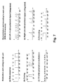
- FIG. 7 An illustration of this kind of back-scatter modulation is given in Fig. 7. It should be noted that the hardware of the data carrier 2 is the same as depicted in Fig. 2. Only the software of the microprocessor 205, 305 on the data carrier 2 has to be modified accordingly.
- the circular polarization-modulated RF carrier from the tag 2 is received by the circular-polarized antenna of the main unit 1.
- the advantage of the circular polarization modulation becomes visible.
- the transmitting linear-polarized antenna 128 of the main unit 1 also couples to the circular-polarized receiving antenna 105, the coupled power is split equally to the left-hand and right-hand circular-polarized antenna ports.
- the demodulation of the circular polarization-modulated waves is executed by comparing the power of the received left-hand and right-hand circular-polarized waves. Therefore a weak circular-polarized signal can be detected even if its power is much lower than the power coupled from the transmitting antenna.
- This embodiment of circular polarization modulation is substantially different from the transmission method disclosed in WO 90/10200.
- the modulation scheme and coding of the back-scattered waves from the data carrier 2 are the same as that for communication from the main unit 1 to the data carrier 2, as shown in Fig. 4. Therefore the receiver 104 - 105, 108 - 127 of the main unit 1 may have the same hardware as the receiver 200 - 204; 300 - 304 of the data carrier 2.
- Fig 6c shows an alternate hardware of the main unit 1. The difference to Fig. 6b is that two double-throw single-pole switches 130, 131 switch the two mutually isolated output ports of the antenna hybrid 104 to two identical demodulation paths 106, 107 comprising an RF preamplifier 108, 109 and an RF detector 110, 111.
- a comparator 132 for demodulation of left and right circular-polarized waves.
- the linear-polarized RF carrier is transmitted by a linear-polarized antenna 128 which can be connected by a switch 129 to a fixed frequency oscillator 102 or to a frequency sweeper 102.
- Fig. 6a - 6c shows some methods for improving the transmission range if the cross-polarization isolation of the main circular-polarized antenna 105 is limiting the required power level of the received back-scattered waves from the data carrier 2.
- demodulation circuits for the back-scattered signal are presented that differ with respect to circuit complexity and detecting sensitivity.
- the apparatus has at least one main unit 1 and one or several sub units 2 that comprise circular-polarized antennas for transmitting and receiving circular-polarized waves and the main unit 1 and the sub unit 2 further comprise means for binary modulation and demodulation of a rotation sense of the circular-polarized waves in at least one communication direction.
- the receivers 104 - 105, 108 - 127, 130 - 132; 200 - 204; 300 - 304 of both the main and sub unit 1, 2 each comprise two receiver channels 106 and 107; 206 and 207; 306 and 307 for demodulation of left and right circular-polarized waves.
- the transmitters 103 - 105; 200, 201, 209 - 211; 300, 301, 308 - 311 of the main and sub unit 1, 2 comprise means for alternately activating 103; 210, 211; 310, 311 orthogonal circular-polarized antenna ports 104, 105; 200, 201; 300, 301.
- a plurality of main units 1 and sub units 2 is provided and the sub units 2 are attachable to objects.
- Communication schemes are presented that are insensitive to circular polarization inversion and that reduce or eliminate cross-talk of the outward-bound RF carrier with the inward-bound polarization-modulated back scatter signals.
- the cross-talking power of a linear-polarized outward-bound carrier is cancelled in the main unit 1 in the two receiver channels 106 and 107 for demodulation of left and right circular-polarized waves.
- linear-polarized jammers are cancelled in the sub unit 2 in the two receiver channels 206 and 207; 306 and 307 for demodulation of left and right circular-polarized waves.
- the method according to invention is particularly useful to transmit test sequences, commands or data from the main unit 1 to the sub unit 2 for the purpose of synchronization, identification, wake-up and request for response.
Abstract
Description
- The invention refers to the field of radio communication for tagging systems. The invention is based on the subject-matter as set forth in the preamble of the
claims 1 and 13. - Radio-frequency identification (RFID) systems serve mainly to manage production lines and manufacturing processes of various kinds of products in a highly efficient way. Data carriers or tags are attached to work pieces transported on a conveyor belt, to a carrying plate such as a pallet or to containers on a railway carriage. The memory of the data carrier contains an identification code of the object the data carrier is attached to, data processing instructions and the like. A number of main apparatuses are arranged along the conveyor belt to conduct communication with the passing data carriers by writing data in or reading data from their memories. After updating the memory of a data carrier, the work piece is transferred to the next production process.
- Microwave tagging systems of the described kind are battery-powered and thus must have a low power consumption at simultaneously low demodulation error rate. These two requirements are often in conflict because modulation schemes with low error rates need power-demanding demodulation circuits. Typical application areas of such microwave tagging systems are manufacturing halls with metallic walls reflecting incident microwaves and hence causing demodulation errors due to multipath propagation, circular polarization inversions and signal fading effects. Therefore a need for safe data transmission in terms of few demodulation errors in combination with low power consumption and small tag dimensions exists.
- In the
EP 0 308 964 A2 an RFID system using tags attached to moving articles is disclosed. The communication between the master or main unit and the tag or sub unit is effected by circular polarized microwaves that are modulated by amplitude shift keying (ASK), phase shift keying (PSK) or frequency shift keying (FSK). In more detail the main unit modulates a first carrier by ASK, generates an unmodulated second carrier of different frequency, mixes both carriers by quadrature phase shift keying (QPSK) and transmits them as a first circular-polarized wave. In the sub unit the waves are separated by QPSK demodulation and the data on the first carrier are demodulated. For backward communication the second carrier is modulated by PSK and optionally FSK, is retransmitted with identical circular polarization and PSK and optionally FSK demodulated in the main unit. Severe drawbacks of this system are its complexity, involving several modulation and demodulation steps and schemes, the need for two frequencies to separate outgoing and incoming waves and the need for several sophisticated, power-consuming components on the sub unit. In order to prolong the battery lifetime on the tag, the main unit can transmit start data on the first carrier using a second, orthogonal circular-polarized wave to awake the tag from a sleep mode. - Another tagging system is described in WO 90/10200 that is based on QPSK modulation in the main and sub unit. The main unit establishes communication by sending a linear polarized wave. In the sub unit a circular-polarized component is received using a circular antenna sensitive to one direction of rotation. For the purpose of tag identification the circular component can be ASK or PSK modulated and amplified by a transistor and echoed back by a circular antenna of opposite direction of rotation. A major problem in this system is the fact that the ASK, PSK or QPSK modulation schemes require a comparison with fixed or absolute signal levels. Therefore linear-polarized jamming signals may cause unacceptably large error rates and make communication impossible.
- Both prior art RFID systems fail to solve the problem of odd numbers of reflections that turn the polarization sense of circular-polarized waves and prohibit a correct demodulation.
- It is the object of the invention to provide a microwave tagging method and apparatus that is operable with reduced power consumption and simultaneously low demodulation error rates and has a simplified construction. This object is achieved according to the invention by the subject-matter as set forth in
claims 1 and 13. - The invention resides in a method and apparatus for radio communication between a main unit and a sub unit, wherein a binary modulation of the rotation sense of circular-polarized waves, i. e. a circular polarization modulation (CPM), is used for the transmission of binary data in at least one communication direction.
- The circular polarization modulation and demodulation (CPM) according to the invention is simpler to implement than conventional FSK modulation schemes and is based on the detection of relative signal levels of left and right circular-polarized waves instead of absolute signal levels as in conventional ASK or PSK modulation schemes. As a consequence the circular polarization modulation (CPM) is largely tolerant against linear-polarized jamming signals. Furthermore the power requirements of the tag are substantially reduced and allow longer battery lifetimes and/or larger communication ranges.
- In one embodiment the receivers of the main and sub unit comprise separate receiver channels for left and right circular-polarized waves. As well the transmitters of the main and sub unit comprise simple means, such as RF switches, for alternately activating orthogonal circular-polarized antenna ports. These measures allow in particular a very simple tag design with few power-saving components.
- In another embodiment the main unit comprises four receiver sections for separate demodulation of left and right circular-polarized waves in different time intervals. The receiver sections may comprise single-sideband downconverters with or without frequency filters to demodulate circular polarization-modulated signals from the sub unit and isolate them from cross-talk and/or integrators to prevent or reduce signal fading.
- In a further embodiment an active sub unit comprises a battery-powered RF amplifier steered by switches to amplify incoming right or left circular-polarized waves and backscatter them with inverted polarization.
- In an alternate embodiment passive sub units are described that simply either absorb incoming waves or transmit them to an orthogonal circular-polarized antenna port.
- A first embodiment referring to the method according to the invention comprises an analysis of the sequential order of bits. In particular binary data are encoded by symbols, which belong to groups that are invariant under binary inversions. Preferentially, in both communication directions two-digit binary symbols are used and are decoded by an EXOR-relation between the digits. These measures render the radio communication insensitive to polarization inversions caused by an uneven number of metallic reflections in the aerial path. Thus the robustness of communication is improved and the signal error rate is decreased.
- A second embodiment referring to the method according to the invention comprises an analysis of the temporal order of bits. In particular a predefined sequence of bit pairs from the main unit is modulated in the sub unit by selectively reflecting either the first or second bit of each bit pair thereby encoding logical values "0" and "1". Preferentially the predefined bit sequence is represented by a sequence of alternating left and right circular-polarized waves. These features further simplify the tag design and secure a reliable communication from the tag to the main unit independent of polarization or bit inversions. Consequently low error rates and high data rates are achieved with minimal power consumption even in time variant paths.
- Other objects, features and advantages of the present invention will be described with reference to the accompanying drawings, in which
- Fig. 1
- is a block diagram of a main unit;
- Fig. 2
- is a block diagram of an active sub unit;
- Fig. 3a, 3b
- are block diagrams of passive sub units;
- Fig. 4
- is an illustration of outward communication from the main to the sub unit;
- Fig. 5 and 7
- are illustrations of inward communication from the sub to the main unit; and
- Fig. 6a-6c
- are block diagrams of modified main units.
- In the drawings identical parts are designated by identical reference numerals.
- In the following embodiments, the system includes a main apparatus or reader or interrogator or
main unit 1, typically located at a predetermined position, and a data carrier or tag or transponder orsub unit 2 attachable to a moving object. When the object carrying thetag 2 passes a position in front of themain unit 1, data is read from or written into thetag memory main unit 1. - A principle of a first embodiment of the present invention will be described with reference to Fig. 1 and Fig. 2. In this first section the transmission of data from the main to the sub unit is explained. Identification data, job processing data, interrogating commands, etc. can be entered by the user to a
computer terminal 100 connected to themain unit 1. Themain apparatus 1 of the first embodiment has amicrowave generator 102, in particular amicrowave oscillator 102 or a frequency sweeper, for the frequency band of interest, for instance the 2.4 GHz, 5.8 GHz or 24 GHz Industrial-Scientific-Medical (ISM) band. According to the present invention the carrier wave of themicrowave oscillator 101 or frequency sweeper is circular polarization modulated correspondingly to the data to be sent to thedata carrier 2. Circular polarization modulation (CPM) can be achieved by modulating bit streams in a way that a logical "0" becomes a right-hand circular-polarized wave R and a logical "1" is attached to a left-hand circular-polarized wave L or vice versa. This kind of modulation scheme is applied for communication in at least one direction, preferentially for outward communication from the main 1 to subunit 2. In particular circular polarization-modulated waves are used in both communication directions. The CPM scheme allows very simple, power-saving and reliable modulation and demodulation circuits, in particular on thetag 2, as will be described further below. - The problem of microwave reflections at metallic walls changing the polarization sense and inducing bit inversions can be overcome in time-invariant paths by exchange of test sequences. For example a wave of long duration emitted with one circular polarization sense can define at the receiving
unit 1, 2 a first circular polarization representing a logical "0", and a wave of short duration emitted with the opposite circular polarization sense can define at the receivingunit 1, 2 a second circular polarization representing a logical "1". - In another preferred embodiment bit-inversion tolerance of the
tag 2 is achieved by a suitable data-encoding scheme. For this purpose the data demodulation shall comprise an analysis of a sequential order of transmitted bits by acontroller 101; 205; 305. In particular, for communication from themain unit 1 to thesub unit 2, logical values "0", "1" of the binary data are encoded in themain unit 1 by multi-bit symbols, such that a plurality of multi-bit symbols are separated into a first and second group to represent a logical "0" and a logical "1" and that the first and second group are both invariant under binary inversions, and after transmission and demodulation the symbols are decoded in thesub unit 2. This symbolic encoding assures bit inversion tolerant communication even in time-variant aerial paths. A particularly simple embodiment will be shown in Fig. 4. - The data sent from the
computer terminal 100 to themain unit 1 is processed on themain unit 1 in acontroller 101 consisting typically of amicro processor 101 which encodes the data stream according to the invention. The circular polarization modulator is simply composed of a double-throw single-pole switch 103 which toggles the microwave carrier of theoscillator 102 or frequency sweeper between its two output ports. These two output ports are connected either to two circular-polarized antennas of opposite polarization sense or to two mutually isolated ports of a 3dB/90°hybrid 104 whose output ports are connected to a dual circular-polarized antenna 105. The axial ratio of the left-hand and right-hand circular-polarized antenna or the dual circular-polarized antenna 105 should be equal to one and the crosspolarization isolation of the circular-polarized antenna ports with opposite polarization sense or the dual-polarizedantenna ports 105 in conjunction with the 3dB/90°hybrid 104 should be as low as possible. By using a frequency sweeper aperture-coupled patch antennas, not shown here, will be preferred because they have a larger bandwidth. - In this second section the reception and demodulation of the transmitted circular polarization-modulated microwave carrier at the
sub unit 2 is described. Thetag 2 possesses either two circular-polarized antennas of opposite polarization sense or preferentially a space-saving dualpolarized antenna 200 in conjunction with a 3dB/90°hybrid 201 for the reception of the circular polarization-modulated carrier wave. It is mentioned here that theantennas 105; 200, 201; 300, 301 serve to transmit and receive essentially circular-polarized waves; slightly elliptical-polarized waves are admissible as well. The demodulation can be simply done by connecting twoidentical RF detectors 202, 203 to the mutually isolated output ports of the 3dB/90°hybrid 201 or the ports of the right-hand and left-hand circular-polarized antenna. TheRF detectors 202, 203 rectify the incident waves of different polarization sense. As is known the output voltage is proportional to the incident power of the wave as long as the rectifyingRF diodes 202, 203 are not operated in the linear detection region. According to the invention the final demodulation of the baseband signal shall be done by comparing the output voltage of the RF detector circuit 202 associated to the reception path of the left-hand circular-polarizedwave 206 to that of theRF detector circuit 203 associated to the reception path of the right-hand circular-polarizedwave 207. The comparison can be done by means of a lowpower CMOS comparator 204 consuming only one or two µA. The output signal of thelow power comparator 204 is sampled by acontroller 205, typically a lowpower micro controller 205. State of the art micro controllers intended for battery-powered applications are consuming about 400 µA in the active mode and about 10 µA in the stand-by mode. For additional power saving a wake-up detector circuit, not shown here, should be incorporated into thetag 2. It may consist of two additional low power comparators that sense the output signal of theRF detector circuits 202, 203 associated to the twopaths control unit 205. - Due to the requirement of low power consumption the
tag 2 should not have microwave local oscillators for mixer circuits, as for example FSK demodulation may require, or RF amplifiers, as for instance PSK demodulation circuits need for carrier recovery. Other RFID systems of prior art, such as inEP 0 308 964 A2, often use ASK modulation because it is easy to implement, even though it shows high demodulation error rates. In contrast the CPM according to invention combines high data rates, low demodulation error rates and reduced sensitivity to jamming signals with a simple, space- and power-saving tag design using few electronic components. As an example consider binary ASK modulation, that can be implemented with similar simple circuit complexity and power requirements as CPM. An important problem with ASK is the choice of the fixed reference or decision threshold voltage. If the threshold is too low, jamming signals easily spoil the demodulation, but if it is too high, thedetection circuitry 202, 203; 302, 303 including preamplifiers on thetag 2 will need too much power. On the contrary the CPM relies on comparing relative signal strengths of left- and right circular-polarized waves in the demodulation paths orreceiver channels receiver channels antenna ports 105; 200; 300 and do not affect the demodulation. Even circular-polarized jamming signals of arbitrary rotation sense are admissible, as long as their strength does not exceed the signal level of the CPM-modulated wave. - In this section the data transmission from the
data carrier 2 to themain unit 1 will be described. According to the goal of the invention to save as much power as possible at the battery-powereddata carrier 2 and under the restriction to an active tagging system in order to obtain a larger transmission distance, a kind of active back-scatter transmission based on an on/off keying modulation of signals with different polarization sense is presented. After the reception of the read out command by themain unit 1, thedata carrier 2 switches itsantenna signal path 208, where theactive modulator 209 is placed. Abattery supply 215 with an activatingswitch 214 is shown as well. As a signal generation by means of a microwave oscillator or voltage-controlled-oscillator (VCO) as frequency sweeper is prohibitively power-consuming, theactive modulator 209 of the first embodiment consists only of anRF amplifier 209 that is normally switched off and can be switched on by means of two double-throw single-pole switches active device 209 is achieved by the crosspolarization isolation of the circularly polarizeddata carrier antenna data carrier 2, themain unit 1 sends out a predefined pattern (Fig. 5) of left-hand and right-hand circularly polarized waves that will be reemitted by thedata carrier 2 provided with the above mentioned modulation. The predefined pattern consists of emitting a first circular-polarized wave of duration T/2 with a polarization sense in one direction and afterwards a second circular-polarized wave of opposite polarization sense. For further explanation of the principle it is assumed that the first wave is left-hand circular-polarized and the second wave is correspondingly right-hand circular-polarized. Besides the left-hand circular-polarized wave is associated to a logical "0" and the right-hand circular-polarized wave is attached to a logical "1". Thus themain unit 1 transmits for each period T a logical "0" of duration T/2 and afterwards a logical "1" of same duration where both "0" and "1" are coded by the polarization sense. Based on this predefined pattern thedata carrier 2 performs - after a short synchronization phase where a test sequence is transmitted to define the start of the read out process - the transmission of its object identification code or memory data back to themain unit 1 in the following way. Thedata carrier 2 receives the predefined wave pattern of themain unit 1 by its circular-polarized antenna main unit 1 to thedata carrier 2. Two double-throw single-pole switches active modulator 209 is connected to the circular-polarized antenna data carrier 2. According to the received predefined pattern theactive modulator 209 is switched either in forward direction connecting the left-hand circular-polarized antenna port with that one generating a right-hand circular-polarized wave or in backward direction connecting the antenna port attached to the reception of a right-hand circular-polarized wave with the antenna port emitting a left-hand circular-polarized wave by means of two single-pole double-throw switches art RF switch RF amplifier 209 used as active modulator consumes a current of 2mA, where both figures are related to the 2.4 GHz ISM band. Theactive modulator 209 uses now on/off keying modulation to modulate and reemit the received waves according to the object identification code or memory data. - If for instance a logical "1" has to be transmitted from the
data carrier 2 to themain unit 1 theRF amplifier 209 amplifies and back-scatters only the circular-polarized wave of the predefined pattern that is associated to a logical "1". For the above made assumptions this means that theactive modulator 209 is switched off during the reception of the first left-hand circular-polarized wave of the predefined pattern which is attached to a logical "0". After T/2 a right-hand circular-polarized wave associated to a logical "1" is emitted by themain unit 1 and theactive modulator 209 is poled in the opposite direction and switched on so that it can receive a right-hand circular-polarized wave and back-scatter the amplified wave as a left-hand circular-polarized wave. That is only during a length of time T/2 of the predefined pattern of duration T a logical "1" or a logical "0" is amplified and reemitted according to the data to be transmitted to themain unit 1. - Polarization errors of the emitted wave patterns are of no importance because they will be eliminated by analyzing the test sequence at the synchronization phase at the beginning of the transmission so that the
amplifier 209 will amplify and reemit the stronger of the two signals appearing at the antenna ports of opposite polarization sense. This can be illustrated by the following example. Themain unit 1 emits a right-hand circular-polarized wave attached to a logical "1". Due to multipath propagation thedata carrier 2 receives at the antenna port associated to the reception of a left-hand circular-polarized wave a stronger signal than at the other antenna port associated to the reception of a right-hand circular-polarized wave. According to the invention thedata carrier 2 defines at the beginning of the transmission a logical "1" as left-hand circular-polarized wave. This definition is valid as long as the channel remains unchanged in terms of the multipath propagation. The freedom of adaptively choosing the polarization sense definition of the reemitted wave affects the demodulation of the data carrier signal at themain unit 1. This will be described in the following section. - The
main unit 1 has two identical receiver channels ordemodulation paths preamplifier RF detector circuit pole switch integrators RF detector circuit demodulation paths antenna ports directional couplers receiver - According to the invention polarization errors shall not affect the demodulation performance as long as the microwave channel can be assumed as time-invariant during the transmission. The demodulation of the data carrier signal, that should be insensitive to bit inversions due to an odd number of reflections in multipath propagation, can be described as follows. First the output signals of the
lower integrators upper integrators hold devices hold devices controller 101. Thecontroller 102 has to find the maximum of the four integrator values. As thelower integrators upper integrator demodulation paths polarized antenna - In this section a second embodiment with a fully
passive data carrier 2 according to invention is described with reference to Fig. 3a and 3b. As shown for theactive data carrier 2 in Fig. 2 thesub unit 2 again comprises a sub receiver 200 - 204; 300 - 304 and asub transmitter antenna 200; 300 connected to a hybrid 201; 301 or two orthogonally circular-polarized antennas for receiving and transmitting left and right circular polarized waves; as well the sub receiver 200 - 204; 300 - 304 further comprises twoRF detectors 202, 203; 302, 303 connected to acomparator 204; 304 in series with thesub controller 205; 305 for comparing signal levels of left and right circular-polarized waves. 315 indicates a long-lived battery. The demodulation of the circular polarization modulated carrier from themain unit 1 is equal to that already described at the first embodiment and does not need any further discussion. However, in the second embodiment of asub transmitter former RF modulator 209, being controllable by activatingmeans pole switches data carrier 2 to themain unit 1 between two usually identical absorbingloads 308 and atransmission line 309a directly connecting the two double-throw single-pole switches pole switches transmission line 309a, an incident left-hand circular-polarized wave is emitted as right-hand circular-polarised wave or vice versa. The two double-throw single-pole switches hybrid 305, that is connected to a dual-polarizedantenna 300, or the antenna ports of two circularly polarized antennas of opposite polarisation sense (not shown) between the receive path, where theRF detectors comparator 304 are located, and the transmitpath 314 with the above described passive modulator 308 - 311. - Similar to the first embodiment the
main unit 1 emits circular polarization modulated waves with a predefined modulation pattern, which is equal to that already described at the first embodiment. After a short synchronization phase, where the double-throw single-pole switches controller 305 adjusts the toggling rate of the double-throw single-pole switches data carrier 2 transmits the data from its memory to themain unit 1 by selectively reflecting or absorbing the received circular polarization modulated waves. - In order to transmit a logical "1" the double-throw single-
pole switches transmission line 309a such that a received left-hand circular-polarized wave is emitted as a right-hand circular-polarized wave and vice versa. During the period of the logical "0" of the predefined modulation pattern the absorbingloads 308 are switched by means of the double-throw single-pole switches 310 - 313 to the output ports of theantenna transmission line 309a is connecting the mutually isolated output ports of the hybrid 305 while themain unit 1 transmits a circular-polarized wave attached to a logical "0" and the absorbingloads 308 are connected to the mutually isolatedhybrid ports 301 during the transmission of a logical "1" of the predefined modulation pattern. The demodulation of the transmitted signals from thedata carrier 2 at themain unit 1 is equal to that already described at the first embodiment. - An alternative
passive data carrier 2 is shown in Fig. 3b. Here thetransmission line 309a is replaced by tworeflectors 309b - 309d, in particular tworeflection phase shifters 309b - 309d. Thereflectors 309b - 309d comprise a 3dB/90°hybrid 309b with a pair of identicalpassive loads reflectors 309b - 309d perform the same function as thetransmission line 309a. In the case ofreflection phase shifters 309b - 309d the waves to be back scattered can be on/off and/or phase-modulated with very little power requirements on thedata carrier 2. - In conclusion, preferred embodiments of both active and
passive sub units 2 according to invention have sub receivers 200 - 204; 300 - 304 andsub transmitters antenna 200; 300 connected to a hybrid 201; 301 or two orthogonal circular-polarized antennas for receiving and transmitting left and right circular polarized waves and the sub receivers 200 - 204; 300 - 304 further comprise twoRF detectors 202, 203; 302, 303 connected to acomparator 204; 304 in series with asub controller 205; 305 for comparing signal levels of left and right circular-polarized waves. The active and passive modulators 209 - 211 and 308 - 311comprise activating means - In this section preferred embodiments of the communication protocol are disclosed. Fig. 4 and 5 depict the communication from the
main unit 1 to thedata carrier 2 and from thedata carrier 2 to themain unit 1 for the case of bit inversion due to an odd number of reflections. A data sequence "01001101" is assumed that represents the ASCII-code for the character "M". The synchronization and test sequence, that generates a weak-up signal for the modulator 209 - 211; 308 - 311 in Fig. 2, 3a and 3b, is not shown. - Fig. 4a depicts the data sequence "01001101" to be transmitted. The bit rate is 1/T. In Fig. 4b the coding of the data sequence is shown. A logical "0" is coded with the symbol "00" and a logical "1" is attached to the symbol "01". By this coding the data rate is halved. As shown in Fig. 4c the symbol "01" representing a logical "1" is transmitted as a right-hand circular-polarized wave R of duration T followed by a left-hand circular-polarized wave L of the same duration. A logical "0", which is attached to the symbol "00", is transmitted correspondingly as two right-hand circular-polarized waves R, R of duration T. In Fig. 4d and 4e the received left-hand and right-hand circular-polarized signals R and L at the
data carrier 2 are shown after bit inversion in the transmission path. Under the assumption that the minus port of thecomparator 204; 304 is connected to the antenna port where the left-hand circular-polarized signal L appears and the plus port of thecomparator 204; 304 is correspondingly connected to the reception path of the right-hand circular-polarized signal R, the output signal of thecomparator 204; 304 has a signal characteristic as shown in Fig. 4f. By changing the connections of the reception paths so that a left-hand circular-polarized signal L is fed to the plus input of thecomparator 204; 304 and the reception path of the right-hand circular-polarized waves R is connected to the minus input the output signal would be inverted compared to the signal characteristic depicted in Fig. 4f. The output signal of thecomparator 204; 304 would also be inverted when a "1" in the symbol of Fig. 4c would be transmitted as a left-hand circular-polarized wave L and a "0" correspondingly as a right-hand circular-polarised wave R. For the demodulation and decoding by means of an EXOR-relation between the bit position 2nT and (2n+1)T as depicted in Fig. 4g this potential inversion of the comparator output signal does not care as "1" ⊕ "1" and "0" ⊕ "0" or "1" ⊕ "0" and "0" ⊕ "1", respectively, are the same. The symbol ⊕ represents the EXOR-relation and n=0, 1, 2, ... an integer. Consequently bit inversions do not affect the demodulation, according to invention, of the transmitted data sequence "01001101". - It should be noted that the output signal of a
comparator 204; 304, which is normally slightly lower than a positive or negative threshold value, can be clipped by a diode so that the output signals become the positive threshold value and zero. In this form the output signal can be better sampled by amicro-controller - The embodiment of Fig. 4 is based on an EXOR-relation where a logical "0" is coded with the two-bit symbols "00" and "11" and a logical "1" is coded with the two-bit symbols "01" and "10". Assuming a time-invariant channel differential coding can also be used where a logical "0" is coded as a transient from a left-hand to a right-hand circular-polarized wave and a logical "1" is assigned correspondingly to the opposite transient or vice versa. According to the invention other encoding schemes are feasible that use multi-bit symbols and are invariant under binary inversions.
- In Fig. 5 the communication from the
data carrier 2 to themain unit 1 is exemplified when a bit inversion occurs in the transmission path. In general a predefined bit pattern is sent by themain unit 1, a plurality of bits or each bit of the bit pattern is on/off- and/or phase-modulated according to the data to be transmitted and is back-scattered by thesub unit 2, and the back-scattered bit pattern is demodulated by themain unit 1. In particular, the bit pattern contains pairs of bits and in thesub unit 2 logical values "0", "1" are modulated onto the bit pattern by back-scattering either the first or the second bit of a bit pair. In a similar way multi-bit representations of the logical values "0" and "1" are feasible. - As shown in Fig. 5a the
data carrier 2 receives a predefined modulation pattern of a continuous sequence of "1"s and "0"s. This sequence may be represented by a sequence of circular-polarized waves with identical or changing rotation sense. In a particularly simple embodiment logical "1"s are transmitted as left-hand circular-polarized waves L and logical "0"s as right-hand circular-polarized waves R. A change or alternation of the rotation sense can be used to detect time-variant paths with changing numbers of reflections. In Fig. 5b the response data sequence "01001101" and in Fig. 5c the circular-polarization modulated signal to be back scattered are depicted. The first bit, in this case the most significant bit, is a logical "0". Therefore the incident right-hand circular-polarized wave is back-scattered as a left-hand circular-polarized wave by means of the tag modulator 209 - 211; 308 - 311 during the time t=0 until t=T/2 when the corresponding logical "0" of the predefined modulation pattern is transmitted. During thetag 2 receiving the left-hand circular-polarized wave of the predefined modulation pattern from t=t/2 to t=T, which is attached to a logical "1", the tag modulator 209 - 211; 308 - 311 is switched off so that no wave is back scattered. - In Fig. 5d and 5e the bit-inverted received signals at the integrator outputs of the
main unit 1 are depicted. The lower integrator of the path where the right-hand circular-polarized signals appear integrates the signals attached to the transmission of a logical "0" in each bit period from t=0 to t=T/2. The upper integrator in the reception path of left-hand circular-polarized signals integrates the signals attached to the transmission of a logical "1" in each bit period from t=T/2 to t=T. - According to Fig. 5f the demodulation and decoding is done by determining the temporal position of the maximum signal value of all four integrator output signals. If the maximum value appears at the lower integrator which is attached to the bit period from t=0 to t=T/2, a logical "0" has been transmitted. If the maximum value appears at the upper integrator, a logical "1" has been transmitted.
- Owing to bit inversions the reception paths or
receiver channels directional couplers main unit 1. In any case a correct demodulation and decoding can be achieved by determination of the temporal position of the maximum integrator output value. - In this last section further embodiments of inward communication and corresponding modifications of the
main unit 1 are described. These embodiments are designed to further improve the isolation between sending and receiving signals at themain unit 1 and in particular to improve the reception of the back-scatter modulated signal. These implementations of themain unit 1 are particularly useful in environments with large signal transmission losses. - A weak reception signal back-scattered from the
data carrier 2 may be difficult to detect with circular-polarized antennas. Due to their relatively poor crosspolarization isolation the separation of the mutually decoupled input ports of the hybrid 104 is too low, and thus the power of the received wave can often be much lower than the power superimposed from the input port. By using amicrostrip hybrid 104 as polarizer a crosspolarization isolation of about 30 dB to 40 dB is feasible. Therefore the transmission distance is mainly limited by the crosspolarization isolation and not by the sensitivity of the receiver circuit itself, which is about -70dBm for a signal with a video bandwidth of 10kHz. For a low cost product a sophisticated and expensive polarizer with improved crosspolarization isolation may probably be undesirable. To enhance the crosspolarization isolation a left-hand and right-hand circular-polarized antenna can be used instead of a single dual-polarised antenna with a hybrid 104 as polarizer. By separating these antennas by about one wavelength a minimum of crosspolarization isolation can be obtained. The disadvantage of such a set-up is that it takes more space. Therefore, some modifications of themain unit 1 are described which can be applied in case that the crosspolarization isolation of the circular-polarized main unit antenna is too low. The presented modifications concern only the communication from thedata carrier 2 to themain unit 1 by means of the back-scatter modulation discussed earlier. A first modification of themain unit 1 of Fig. 1 is described with reference to Fig. 6a, where theRF detectors mixers sub unit main unit 1 of Fig. 1 is described with reference to Fig. 6b and 6c. In Fig. 6b the only modification compared to Fig. 1 is that the RF carrier for the back-scatter modulation is transmitted by an additional linear-polarizedantenna 128 that is connected to themicrowave generator 102 by anadditional switch 129. The rest of the hardware of the main andsub unit main unit 1 according to Fig. 6b, where some parts of the receiver hardware are omitted or simplified. - The fist modification of the receiving part of the
main unit 1 is depicted in Fig. 6a. The idea of this modification is to get rid of the disturbing cross-talk power from the mutually isolated port of the hybrid 104. This can be done by detecting in themain unit 1 only the power of sidebands of the circular polarization-modulated signal from thesub unit 2. The sidebands are caused by the switching function of the modulating data sequence on thedata carrier 2. - A very simple solution (not shown) is to use series capacitances between the
RF detector diodes - Another solution is depicted in Fig. 6a. As the sensitivity of detector diodes is much lower than the sensitivity of mixers used as detectors, the
detectors sideband downconverters sideband mixers data carrier 2 from themain unit 1 by a multiple of its wavelength. Low-frequency bandpass filters 126, 127 at the intermediate frequency port of the single-sideband mixers sideband mixers microstrip hybrid 104 used as polarizer for the circular-polarized antenna. Moreover the sensitivity of themixers data carrier 2, is about 40 dB to 50 dB better than for the simple solution of cross-talk suppression by a series-capacitance after theRF detector diodes RF detector diode frequency bandpass filter - The second modification of the
main unit 1 describes another simple method to circumvent the problem of poor crosspolarization isolation, wherein a linear-polarized antenna is used at themain unit 1 to transmit an unmodulated linear-polarized RF carrier for back-scatter modulation by thedata carrier 2. As shown below the coupling between the linear-polarized and circular-polarized antennas of themain unit 1 does not affect the reception and demodulation of circular polarization-modulated signals from thesub unit 2. - The
tag 2 receives the linear-polarized RF carrier with its circular-polarized antenna data carrier 2 performs the circular polarization modulation as already described in the communication from themain unit 1 to thetag 2. Preferentially the binary data from thedata carrier 2 are coded to be insensitive to polarization inversions during transmission by the symbols "00" or "11" and "10" or "01" as described above. The zeros and ones in the symbols are transmitted as left-hand or right-hand circular-polarized waves. If a one has to be transmitted the modulator 209 - 211; 308, 309a; 308, 309b - 309d, in particular theactive modulator 209, feeds the received possibly amplified linear-polarized wave appearing at the right-hand circular-polarized port to the antenna port that emits a left-hand circular-polarized wave. A zero is transmitted correspondingly as a wave of opposite polarization sense. An illustration of this kind of back-scatter modulation is given in Fig. 7. It should be noted that the hardware of thedata carrier 2 is the same as depicted in Fig. 2. Only the software of themicroprocessor data carrier 2 has to be modified accordingly. - The circular polarization-modulated RF carrier from the
tag 2 is received by the circular-polarized antenna of themain unit 1. Now the advantage of the circular polarization modulation becomes visible. As the transmitting linear-polarizedantenna 128 of themain unit 1 also couples to the circular-polarized receiving antenna 105, the coupled power is split equally to the left-hand and right-hand circular-polarized antenna ports. As described above the demodulation of the circular polarization-modulated waves is executed by comparing the power of the received left-hand and right-hand circular-polarized waves. Therefore a weak circular-polarized signal can be detected even if its power is much lower than the power coupled from the transmitting antenna. This embodiment of circular polarization modulation is substantially different from the transmission method disclosed in WO 90/10200. Even though a linear-polarized carrier is transmitted by the main unit and is back-scattered by the data carrier as circular-polarized wave in WO 90/10200 as well, the problem of cross-coupling between the transmission and reception antenna of the main unit is unsolved as the demodulation of the back-scattered ASK-modulated circular-polarized waves actually requires a very high polarization isolation between the linear-polarized transmitting and receiving antennas. Practical measurements showed that the transmission distance of this system is still limited by the coupling between the linear-polarized main unit antennas and not by the sensitivity of the RF receiver, as is the case with the circular polarization modulation according to this invention. The demodulation of the circular polarization-modulated signal at themain unit 1 can be done by the same hardware as shown in Fig. 1. That is, thelower integrators upper integrators microprocessor 101 of themain unit 1 reads the output values of the sample-and-hold devices lower integrators hold devices upper integrators same demodulation path main unit 1 remains as in Fig.1, except the additional linear-polarizedtransmission antenna 128 in Fig. 6b and 6c. Only the software of themain controller 101 must be modified. Furthermore it is emphasized that signal integration can be abandoned if the expected level of signal fading is sufficiently low. - As mentioned above the modulation scheme and coding of the back-scattered waves from the
data carrier 2 are the same as that for communication from themain unit 1 to thedata carrier 2, as shown in Fig. 4. Therefore the receiver 104 - 105, 108 - 127 of themain unit 1 may have the same hardware as the receiver 200 - 204; 300 - 304 of thedata carrier 2. Fig 6c shows an alternate hardware of themain unit 1. The difference to Fig. 6b is that two double-throw single-pole switches antenna hybrid 104 to twoidentical demodulation paths RF preamplifier RF detector identical demodulation paths comparator 132 for demodulation of left and right circular-polarized waves. In particular the comparator output signal is sampled by thecontroller 101 that demodulates and decodes the sampled data sequence by executing an EXOR-relation between the bit at the time t=2nT and t=(2n+1)T. Again the linear-polarized RF carrier is transmitted by a linear-polarizedantenna 128 which can be connected by aswitch 129 to a fixedfrequency oscillator 102 or to afrequency sweeper 102. - The above description of the
main unit 1 according to Fig. 6a - 6c shows some methods for improving the transmission range if the cross-polarization isolation of the main circular-polarized antenna 105 is limiting the required power level of the received back-scattered waves from thedata carrier 2. Several demodulation circuits for the back-scattered signal are presented that differ with respect to circuit complexity and detecting sensitivity. - In summary the apparatus according to invention has at least one
main unit 1 and one orseveral sub units 2 that comprise circular-polarized antennas for transmitting and receiving circular-polarized waves and themain unit 1 and thesub unit 2 further comprise means for binary modulation and demodulation of a rotation sense of the circular-polarized waves in at least one communication direction. Preferentially the receivers 104 - 105, 108 - 127, 130 - 132; 200 - 204; 300 - 304 of both the main andsub unit receiver channels sub unit polarized antenna ports main units 1 andsub units 2 is provided and thesub units 2 are attachable to objects. Communication schemes are presented that are insensitive to circular polarization inversion and that reduce or eliminate cross-talk of the outward-bound RF carrier with the inward-bound polarization-modulated back scatter signals. In particular the cross-talking power of a linear-polarized outward-bound carrier is cancelled in themain unit 1 in the tworeceiver channels sub unit 2 in the tworeceiver channels main unit 1 to thesub unit 2 for the purpose of synchronization, identification, wake-up and request for response. - It should be emphasized that arbitrary combinations of the features according to invention, such as unidirectional or bidirectional circular polarization modulation, symbol encoding for outward and/or inward communication, time encoding for inward communication and the use of active or
passive tags 2 are feasible and each have specific merits.
Claims (22)
- A method for radio communication between a main unit (1) and a sub unit (2), where binary data are exchanged in the form of bit sequences by means of modulated RF waves or microwaves, characterized in that for communication in at least one direction the waves are circular polarization-modulated such that bits of information to be communicated ("0", "1") are represented by orthogonal circular polarizations (R, L).
- The method for radio communication according to claim 1, wherein the waves are circular polarization-modulated in both communication directions.
- The method for radio communication according to one of the claims 1 - 2, wherein demodulating the data comprises the step of analyzing (101; 205; 305) a sequential order and/or temporal positions of transmitted bits.
- The method for radio communication according to one of the claims 1 - 3, wherein for communication from the main unit (1) to the sub unit (2) and/or for communication from the sub unit (2) to the main unit (1)a) logical values ("0", "1") of the binary data are encoded by multi-bit symbols such thatb) a plurality of multi-bit symbols are separated into a first and second group to represent a logical "0" and a logical "1" and that the first and second group are both invariant under binary inversions, andc) after transmission and demodulation the symbols are decoded in the sub unit (2).
- The method for radio communication according to claim 4, whereina) one logical value ("0", "1") is encoded by a first symbol with two identical bits ("11", "00") that are transmitted as a sequence of two equally circular-polarized waves (RR, LL) of duration T each,b) the other logical value ("1", "0") is encoded by a second symbol with two different bits ("10", "01") that are transmitted as a sequence of two differently circular-polarized waves (RL, LR) of duration T each andc) after transmission and demodulation of the symbols the logical values ("0", "1") are decoded by comparing (205; 305) the bits of each symbol with an EXOR-relation.
- The method for radio communication according to one of the claims 1 - 5, wherein the communication from the sub unit (2) to the main unit (1) comprises the following steps:a) a predefined bit pattern is sent by the main unit (1),b) each bit of the bit pattern is on/off- and/or phase-modulated according to the data to be transmitted and is back-scattered by the sub unit (2) andc) the back-scattered bit pattern is demodulated by the main unit (1).
- The method for radio communication according to claim 6, whereina) the bit pattern contains pairs of bits andb) in the sub unit (2) logical values ("0", "1") are modulated onto the bit pattern by back-scattering either the first or the second bit of a bit pair.
- The method for radio communication according to claim 7, whereina) the bit pattern consists of left and right circular-polarized waves, that are emitted alternately during half intervals T/2 and represent a first logical value ("0", "1") in first time intervals 0...T/2 and a second logical value ("1", "0") in second time intervals T/2...T,b) the pattern is on/off modulated such that either a first or second logical value ("0", "1") is back scattered by the sub unit (2) during time intervals 0...T andc) the data are demodulated by comparing signals of both left and right circular-polarized waves during first time intervals 0...T/2 with those of second time intervals T/2...T.
- The method for radio communication according to one of the claims 1 - 8, wherein for communication from the sub unit (2) to the main unit (1) only power of a sideband of a circular polarization-modulated signal from the sub unit (2) is detected by the main unit (1).
- The method for radio communication according to one of the claims 1 - 5, wherein the communication from the sub unit (2) to the main unit (1) comprises the following steps:a) an unmodulated linear-polarized RF carrier is transmitted by the main unit (1),b) the RF carrier is split in left and right circular-polarized waves, is circular polarization-modulated and is back-scattered by the sub unit (2) andc) the circular polarization-modulated RF carrier is received by a circular-polarized antenna of the main unit (1) and is demodulated.
- The method for radio communication according to one of the claims 1 - 10, whereina) the sub unit (2) is battery-powered (214, 215) andb) in the sub unit (2) incoming waves are amplified by an RF amplifier (209) and back scattered with orthogonal circular polarization.
- The method for radio communication according to one of the claims 1 - 11, whereina) in the main unit (1) the step of demodulation includes signal integration (114 - 117) to minimize fading and/orb) test sequences, commands or data are sent from the main unit (1) to the sub unit (2) for the purpose of synchronization, identification, wake-up and request for response.
- A signal transmission apparatus for radio communication between at least one main unit (1) and at least one sub unit (2), in particular suitable for implementation of the method according to one of the claims 1 - 12, comprising said at least one main unit (1) with a controller (101) to control a microwave generator (102), a transmitter (103 - 105, 128 - 129) and a receiver (104 - 105, 108 - 127, 130 - 132), and said at least one sub unit (2) with a sub controller (205; 305) to control a sub transmitter (200, 201, 209 - 211; 300, 301, 308 - 311) and a sub receiver (200 - 204; 300 - 304), wherein
the main unit (1) and the sub unit (2) comprise antennas for transmitting and receiving circular-polarized waves for communication between said at least one main unit (1) and said at least one sub unit (2),
the signal transmission apparatus being characterised in that
said at least one
main unit (1) and said at least one sub unit (2) further comprise means for binary modulation and demodulation of a rotation sense of the circular-polarized waves to be transmitted and received in at least one communication direction - The signal transmission apparatus according to claim 13, wherein the receivers (104 - 105, 108 - 127, 130 - 132; 200 - 204; 300 - 304) of the main and sub unit (1, 2) comprise two receiver channels (106 and 107; 206 and 207; 306 and 307) for demodulation of left and right circular-polarized waves.
- The signal transmission apparatus according to one of the claims 13 - 14, wherein the transmitters (103 - 105; 200, 201, 209 - 211; 300, 301, 308 - 311) of the main and sub unit (1, 2) comprise means for alternately activating (103; 210, 211; 310, 311) orthogonal circular-polarized antenna ports (104, 105; 200, 201; 300, 301).
- The signal transmission apparatus according to one of the claims 13 - 15, wherein in the main unit (1)a) the microwave generator (102) is a microwave oscillator (102) or a microwave frequency sweeper,b) the transmitter (103 - 105, 128 - 129) and the receiver (104 - 105, 108 - 127, 130 - 132) comprise either a dual circular-polarized antenna (105) connected to a hybrid (104) or two orthogonal circular-polarized antennas andc) in particular the transmitter (103 - 105, 128 - 129) comprises an additional linear-polarized antenna (128) switchably (129) connected to the microwave generator (102) for transmitting a linear-polarized RF carrier.
- The signal transmission apparatus according to claim 16, whereina) the receiver (104 - 105, 108 - 127, 130 - 132) further comprises two preamplifiers (108, 109) followed by either RF detectors (110 - 111) with optional series capacitances or by single-sideband mixers (124, 125) with low-frequency bandpass filters (126, 127), which detectors (110 - 111) or mixers (124, 125) are switchably (112, 113) connected to four receiver sections (114, 120; 115, 121; 116, 122; 117, 123) for separate demodulation of left and right circular-polarized waves in different time intervals orb) the receiver (104 - 105, 108 - 127, 130 - 132) further comprises two preamplifiers (108, 109) followed by RF detectors (110 - 111), that are connected to a comparator (132) for demodulation of left and right circular-polarized waves.
- The signal transmission apparatus according to one of the claims 16 - 17, whereina) each receiver section (114, 120; 115, 121; 116, 122; 117, 123) comprises an integrator (114 - 117) to prevent signal fading and/orb) directional couplers (118, 119) or double-throw single-pole switches (130, 131) separate the transmitter (103 - 105) and the receiver (104 - 105, 108 - 127, 130 - 132).
- The signal transmission apparatus according to one of the claims 13 - 18, wherein in the sub unit (2)a) the sub receiver (200 - 204; 300 - 304) and the sub transmitter (200, 201, 209 - 211; 300, 301, 308 - 311) comprise either a dual-polarized antenna (200; 300) connected to a hybrid (201; 301) or two orthogonal circular-polarized antennas for receiving and transmitting left and right circular-polarized waves andb) the sub receiver (200 - 204; 300 - 304) further comprises two RF detectors (202, 203; 302, 303) connected to a comparator (204; 304) in series with the sub controller (205; 305) for comparing signal levels of left and right circular-polarized waves.
- The signal transmission apparatus according to one of the claims 13 - 19, whereina) the sub unit (2) has a battery supply (214, 215) andb) the sub transmitter (200, 201, 209 - 211) comprises an RF amplifier (209) that is controllable by activating means (210, 211, 205) for selective amplification and back-scattering of left or right circular-polarized waves.
- The signal transmission apparatus according to one of the claims 13 - 19, wherein the sub transmitter (300, 301, 308 - 311) comprises two absorbing loads (308) and a transmission line (309a) that can alternately be activated by activating means (310, 311, 305) for selective back-scattering of left or right circular-polarized waves.
- The signal transmission apparatus according to one of the claims 13 - 19, wherein the sub transmitter (300, 301, 308 - 311) comprises two absorbing loads (308) and two reflectors (309b - 309d), in particular reflection phase shifters (309b - 309d), that can alternately be activated by activating means (310, 311, 305) for selective back-scattering of left or right circular-polarized waves.
Priority Applications (3)
| Application Number | Priority Date | Filing Date | Title |
|---|---|---|---|
| AT98118821T ATE347714T1 (en) | 1998-10-05 | 1998-10-05 | MICROWAVE LABELING SYSTEM |
| DE69836583T DE69836583T2 (en) | 1998-10-05 | 1998-10-05 | Microwave labeling system |
| EP98118821A EP0992931B1 (en) | 1998-10-05 | 1998-10-05 | Microwave tagging system |
Applications Claiming Priority (1)
| Application Number | Priority Date | Filing Date | Title |
|---|---|---|---|
| EP98118821A EP0992931B1 (en) | 1998-10-05 | 1998-10-05 | Microwave tagging system |
Publications (2)
| Publication Number | Publication Date |
|---|---|
| EP0992931A1 EP0992931A1 (en) | 2000-04-12 |
| EP0992931B1 true EP0992931B1 (en) | 2006-12-06 |
Family
ID=8232753
Family Applications (1)
| Application Number | Title | Priority Date | Filing Date |
|---|---|---|---|
| EP98118821A Expired - Lifetime EP0992931B1 (en) | 1998-10-05 | 1998-10-05 | Microwave tagging system |
Country Status (3)
| Country | Link |
|---|---|
| EP (1) | EP0992931B1 (en) |
| AT (1) | ATE347714T1 (en) |
| DE (1) | DE69836583T2 (en) |
Families Citing this family (5)
| Publication number | Priority date | Publication date | Assignee | Title |
|---|---|---|---|---|
| EP2058955A4 (en) * | 2006-09-11 | 2009-10-28 | Hitachi Ltd | Radio frequency identification ic tag reader and radio frequency identification ic tag system |
| US8285214B2 (en) * | 2008-03-10 | 2012-10-09 | Pepperl + Fuchs Gmbh | Adjustable circuit and RFID reader device |
| US8472560B2 (en) * | 2010-11-02 | 2013-06-25 | Securekey Technologies Inc. | Apparatus and method for detecting RFID signals |
| US10430783B2 (en) | 2016-10-03 | 2019-10-01 | Square, Inc. | Transmit phase detection circuit |
| USD812130S1 (en) | 2016-10-28 | 2018-03-06 | Square, Inc. | Electronic device |
Family Cites Families (2)
| Publication number | Priority date | Publication date | Assignee | Title |
|---|---|---|---|---|
| EP0308964B1 (en) * | 1987-09-24 | 1994-05-04 | Fujitsu Limited | Radio-frequency identification system |
| FR2682546B1 (en) * | 1991-10-15 | 1994-11-18 | Thomson Composants Microondes | SYSTEM FOR TRANSMITTING DATA BY EXCHANGING MICROWAVE WAVES. |
-
1998
- 1998-10-05 EP EP98118821A patent/EP0992931B1/en not_active Expired - Lifetime
- 1998-10-05 AT AT98118821T patent/ATE347714T1/en not_active IP Right Cessation
- 1998-10-05 DE DE69836583T patent/DE69836583T2/en not_active Expired - Lifetime
Also Published As
| Publication number | Publication date |
|---|---|
| EP0992931A1 (en) | 2000-04-12 |
| ATE347714T1 (en) | 2006-12-15 |
| DE69836583D1 (en) | 2007-01-18 |
| DE69836583T2 (en) | 2007-06-21 |
Similar Documents
| Publication | Publication Date | Title |
|---|---|---|
| US6686830B1 (en) | Homodyne I/Q transceiver for a spread spectrum reader | |
| US4926187A (en) | Radio-frequency identification system | |
| Kossel et al. | An active tagging system using circular-polarization modulation | |
| US20040203478A1 (en) | Rfid receiver apparatus and method | |
| US7714773B2 (en) | RFID tag distance measuring system and reader | |
| US8292175B2 (en) | Tag device, reader device, and RFID system | |
| US20080001783A1 (en) | Method and apparatus for detecting a path of travel or direction of travel | |
| US20090305628A1 (en) | Method of obtaining single wire transmission line | |
| US8285224B2 (en) | Transmitter/receiver for radio communication, RFID system and receiving method for transmitter/receiver for radio communication | |
| US7209040B2 (en) | Homodyne RFID receiver and method | |
| US6731199B1 (en) | Non-contact communication system | |
| US5164719A (en) | Radio system for data transmission with passive terminal station | |
| US5533045A (en) | Automatic vehicle identification system, interrogator and responder included in the same | |
| EP0992931B1 (en) | Microwave tagging system | |
| JPH02178893A (en) | Proximity reading of tag coded | |
| CN113748571A (en) | Method and system for controlling modal antenna | |
| JP2005209002A (en) | Ic tag reader/writer, and apparatus having the same | |
| JP2000090215A (en) | Reader/writer and non-contact ic card system | |
| US20230115786A1 (en) | METHOD AND SYSTEM FOR LONG RANGE Wi-Fi BACKSCATTER COMMUNICATION | |
| JP2004088755A (en) | Communication system, interrogator and transponder of the communication system | |
| US20100207733A1 (en) | Method for classifying a transponder and/or signals from a transponder and reader | |
| JPH0690194A (en) | Simultaneous data transmitting-receiving system using microwaves | |
| US7982607B2 (en) | Method and apparatus for handling wireless transmissions from a tag | |
| JP4680093B2 (en) | Electronic tag system | |
| KR102485870B1 (en) | Antenna-separated high-pass terminal |
Legal Events
| Date | Code | Title | Description |
|---|---|---|---|
| PUAI | Public reference made under article 153(3) epc to a published international application that has entered the european phase |
Free format text: ORIGINAL CODE: 0009012 |
|
| AK | Designated contracting states |
Kind code of ref document: A1 Designated state(s): AT CH DE DK ES FI FR GB IT LI SE |
|
| AX | Request for extension of the european patent |
Free format text: AL;LT;LV;MK;RO;SI |
|
| 17P | Request for examination filed |
Effective date: 20000707 |
|
| AKX | Designation fees paid |
Free format text: AT CH DE DK ES FI FR GB IT LI SE |
|
| GRAP | Despatch of communication of intention to grant a patent |
Free format text: ORIGINAL CODE: EPIDOSNIGR1 |
|
| GRAS | Grant fee paid |
Free format text: ORIGINAL CODE: EPIDOSNIGR3 |
|
| GRAA | (expected) grant |
Free format text: ORIGINAL CODE: 0009210 |
|
| AK | Designated contracting states |
Kind code of ref document: B1 Designated state(s): AT CH DE DK ES FI FR GB IT LI SE |
|
| PG25 | Lapsed in a contracting state [announced via postgrant information from national office to epo] |
Ref country code: LI Free format text: LAPSE BECAUSE OF FAILURE TO SUBMIT A TRANSLATION OF THE DESCRIPTION OR TO PAY THE FEE WITHIN THE PRESCRIBED TIME-LIMIT Effective date: 20061206 Ref country code: IT Free format text: LAPSE BECAUSE OF FAILURE TO SUBMIT A TRANSLATION OF THE DESCRIPTION OR TO PAY THE FEE WITHIN THE PRESCRIBED TIME-LIMIT;WARNING: LAPSES OF ITALIAN PATENTS WITH EFFECTIVE DATE BEFORE 2007 MAY HAVE OCCURRED AT ANY TIME BEFORE 2007. THE CORRECT EFFECTIVE DATE MAY BE DIFFERENT FROM THE ONE RECORDED. Effective date: 20061206 Ref country code: FI Free format text: LAPSE BECAUSE OF FAILURE TO SUBMIT A TRANSLATION OF THE DESCRIPTION OR TO PAY THE FEE WITHIN THE PRESCRIBED TIME-LIMIT Effective date: 20061206 Ref country code: DK Free format text: LAPSE BECAUSE OF FAILURE TO SUBMIT A TRANSLATION OF THE DESCRIPTION OR TO PAY THE FEE WITHIN THE PRESCRIBED TIME-LIMIT Effective date: 20061206 Ref country code: CH Free format text: LAPSE BECAUSE OF FAILURE TO SUBMIT A TRANSLATION OF THE DESCRIPTION OR TO PAY THE FEE WITHIN THE PRESCRIBED TIME-LIMIT Effective date: 20061206 Ref country code: AT Free format text: LAPSE BECAUSE OF FAILURE TO SUBMIT A TRANSLATION OF THE DESCRIPTION OR TO PAY THE FEE WITHIN THE PRESCRIBED TIME-LIMIT Effective date: 20061206 |
|
| REG | Reference to a national code |
Ref country code: GB Ref legal event code: FG4D |
|
| REG | Reference to a national code |
Ref country code: CH Ref legal event code: EP |
|
| REF | Corresponds to: |
Ref document number: 69836583 Country of ref document: DE Date of ref document: 20070118 Kind code of ref document: P |
|
| RAP2 | Party data changed (patent owner data changed or rights of a patent transferred) |
Owner name: IDENTEC SOLUTIONS AG |
|
| PG25 | Lapsed in a contracting state [announced via postgrant information from national office to epo] |
Ref country code: SE Free format text: LAPSE BECAUSE OF FAILURE TO SUBMIT A TRANSLATION OF THE DESCRIPTION OR TO PAY THE FEE WITHIN THE PRESCRIBED TIME-LIMIT Effective date: 20070306 |
|
| PG25 | Lapsed in a contracting state [announced via postgrant information from national office to epo] |
Ref country code: ES Free format text: LAPSE BECAUSE OF FAILURE TO SUBMIT A TRANSLATION OF THE DESCRIPTION OR TO PAY THE FEE WITHIN THE PRESCRIBED TIME-LIMIT Effective date: 20070317 |
|
| REG | Reference to a national code |
Ref country code: CH Ref legal event code: PL |
|
| EN | Fr: translation not filed | ||
| PLBE | No opposition filed within time limit |
Free format text: ORIGINAL CODE: 0009261 |
|
| STAA | Information on the status of an ep patent application or granted ep patent |
Free format text: STATUS: NO OPPOSITION FILED WITHIN TIME LIMIT |
|
| 26N | No opposition filed |
Effective date: 20070907 |
|
| PG25 | Lapsed in a contracting state [announced via postgrant information from national office to epo] |
Ref country code: FR Free format text: LAPSE BECAUSE OF FAILURE TO SUBMIT A TRANSLATION OF THE DESCRIPTION OR TO PAY THE FEE WITHIN THE PRESCRIBED TIME-LIMIT Effective date: 20070727 |
|
| GBPC | Gb: european patent ceased through non-payment of renewal fee |
Effective date: 20071005 |
|
| PG25 | Lapsed in a contracting state [announced via postgrant information from national office to epo] |
Ref country code: GB Free format text: LAPSE BECAUSE OF NON-PAYMENT OF DUE FEES Effective date: 20071005 Ref country code: FR Free format text: LAPSE BECAUSE OF FAILURE TO SUBMIT A TRANSLATION OF THE DESCRIPTION OR TO PAY THE FEE WITHIN THE PRESCRIBED TIME-LIMIT Effective date: 20061206 |
|
| PGFP | Annual fee paid to national office [announced via postgrant information from national office to epo] |
Ref country code: DE Payment date: 20121219 Year of fee payment: 15 |
|
| REG | Reference to a national code |
Ref country code: DE Ref legal event code: R119 Ref document number: 69836583 Country of ref document: DE Effective date: 20140501 |
|
| PG25 | Lapsed in a contracting state [announced via postgrant information from national office to epo] |
Ref country code: DE Free format text: LAPSE BECAUSE OF NON-PAYMENT OF DUE FEES Effective date: 20140501 |