EP0991797B1 - Verfahren und vorrichtung zur herstellung elektrisch leitfähiger durchgänge in halbleiter-bauelementen - Google Patents
Verfahren und vorrichtung zur herstellung elektrisch leitfähiger durchgänge in halbleiter-bauelementen Download PDFInfo
- Publication number
- EP0991797B1 EP0991797B1 EP98943631A EP98943631A EP0991797B1 EP 0991797 B1 EP0991797 B1 EP 0991797B1 EP 98943631 A EP98943631 A EP 98943631A EP 98943631 A EP98943631 A EP 98943631A EP 0991797 B1 EP0991797 B1 EP 0991797B1
- Authority
- EP
- European Patent Office
- Prior art keywords
- semiconductor
- specimen
- temperature
- cooling
- head
- Prior art date
- Legal status (The legal status is an assumption and is not a legal conclusion. Google has not performed a legal analysis and makes no representation as to the accuracy of the status listed.)
- Expired - Lifetime
Links
Images


Classifications
-
- H—ELECTRICITY
- H10—SEMICONDUCTOR DEVICES; ELECTRIC SOLID-STATE DEVICES NOT OTHERWISE PROVIDED FOR
- H10P—GENERIC PROCESSES OR APPARATUS FOR THE MANUFACTURE OR TREATMENT OF DEVICES COVERED BY CLASS H10
- H10P95/00—Generic processes or apparatus for manufacture or treatments not covered by the other groups of this subclass
- H10P95/50—Alloying conductive materials with semiconductor bodies
-
- H—ELECTRICITY
- H10—SEMICONDUCTOR DEVICES; ELECTRIC SOLID-STATE DEVICES NOT OTHERWISE PROVIDED FOR
- H10P—GENERIC PROCESSES OR APPARATUS FOR THE MANUFACTURE OR TREATMENT OF DEVICES COVERED BY CLASS H10
- H10P72/00—Handling or holding of wafers, substrates or devices during manufacture or treatment thereof
- H10P72/04—Apparatus for manufacture or treatment
- H10P72/0431—Apparatus for thermal treatment
- H10P72/0436—Apparatus for thermal treatment mainly by radiation
-
- H—ELECTRICITY
- H10—SEMICONDUCTOR DEVICES; ELECTRIC SOLID-STATE DEVICES NOT OTHERWISE PROVIDED FOR
- H10F—INORGANIC SEMICONDUCTOR DEVICES SENSITIVE TO INFRARED RADIATION, LIGHT, ELECTROMAGNETIC RADIATION OF SHORTER WAVELENGTH OR CORPUSCULAR RADIATION
- H10F77/00—Constructional details of devices covered by this subclass
- H10F77/93—Interconnections
- H10F77/933—Interconnections for devices having potential barriers
-
- H—ELECTRICITY
- H10—SEMICONDUCTOR DEVICES; ELECTRIC SOLID-STATE DEVICES NOT OTHERWISE PROVIDED FOR
- H10W—GENERIC PACKAGES, INTERCONNECTIONS, CONNECTORS OR OTHER CONSTRUCTIONAL DETAILS OF DEVICES COVERED BY CLASS H10
- H10W20/00—Interconnections in chips, wafers or substrates
- H10W20/01—Manufacture or treatment
- H10W20/021—Manufacture or treatment of interconnections within wafers or substrates
- H10W20/023—Manufacture or treatment of interconnections within wafers or substrates the interconnections being through-semiconductor vias
Definitions
- the invention relates to a method of manufacture electrically conductive passages in semiconductor components and on a device for performing the Process.
- US-A-4 159 215 discloses a method of penetration one made of doped silicon, germanium or the like existing semiconducting base body of a semiconductor component, the opposing surfaces has, with an alloy with aluminum as the carrier material and phosphorus, arsenic or antimony as a doping agent Temperature gradient zone melting is known.
- the semiconductor device is placed in a metal vapor chamber and an aluminum-antimony layer with a layer thickness of 0.5 ⁇ m - 25 ⁇ m on one of the two surfaces of the Semiconductor component applied. Using photolithography the migration areas are determined and so prepared component in a thermal migration device arranged.
- Such from one surface to the opposite Channels running on the surface of a semiconductor component are used especially with SMD (Surface Mounted Devices) components used, which are designed so that the contact points both electrodes on one surface (the Rear) of the component can be arranged. On such component can with its back to a suitable printed circuit board connected without additional wires or other fasteners are needed.
- SMD Surface Mounted Devices
- a special area of application is optoelectronic sensor components, i.e. Radiation receiver, the electromagnetic Radiant energy (photons) in electrical signals convert and are of great importance in measurement technology.
- Radiation receiver the electromagnetic Radiant energy (photons) in electrical signals convert and are of great importance in measurement technology.
- position measuring systems such as lengths and Angle measuring systems (incremental or absolute) several radiation receivers behind a lattice structure (especially photo elements) arranged.
- Radiation receivers of this type are generally used as junction photodetectors educated. They contain one PN, PIN, MS or MOS transition in which the conversion electromagnetic radiation energy into an electrical Signal by means of the photo barrier layer effect. To do that To be able to measure and evaluate electrical signals, the Provide radiation receivers with electrical contacts be and connected to a suitable electrical circuit become. This integration into an electrical circuit often takes place on a printed circuit board, the radiation receiver preferably designed as SMD components are.
- a cylindrical, semiconducting p-type channel between the p-type Layer and the back surface of the semiconductor device manufactured which preferably has a diameter from 30 ⁇ m to 100 ⁇ m and among others Connection process using thermomigration can be.
- thermomigration is based on the fact that the solubility metallic dopants in semiconducting Materials such as Silicon, is temperature dependent and increases with increasing temperature. Will be between two opposite surfaces of a sufficiently heated Semiconductor component generates a temperature gradient and a suitable one on the cooler surface of the component metallic dopant applied (e.g. aluminum for p-doping n-type regions), the migrates metallic dopant to the opposite, warmer surface of the semiconductor device.
- a suitable one on the cooler surface of the component metallic dopant applied e.g. aluminum for p-doping n-type regions
- the shape of such channels can be set specifically.
- WO 83 03710 describes a method for carrying out the Thermomigration process described on semiconductors, at which the correspondingly prepared semiconductor with one Surface onto a substantially flat surface of a Heat source is placed so that it is on the surface of the heat source is applied. The half-egg is heated, one Temperature difference between the two surfaces of the Semiconductor is built. Applied to the semiconductor Drops of oppositely conductive material migrate as through the semiconductor and form conductive connections between the two surfaces. Then that will Cooled heating element and removed the semiconductor. By the direct contact between the semiconductor and the heat source a high temperature gradient is generated in the semiconductor and thus accelerated the process.
- the disadvantage of the prior art is that it is uniform Temperature control is hardly possible in this way.
- the invention was based on this prior art based on the task in the production of Semiconductor components using thermomigration adjustment Surface temperature of the semiconductor during the Perform the procedure so that a safe Penetration of conductive through channels through the semiconductor wafer with fixed pn transitions in minimal time - is possible without the doping of the semiconductor components affected by the heating of the semiconductor wafer are changed or the shape of the semiconductor wafer becomes. In addition, interactions between the Surface of the heat source or the cooling device and the Wafers can be avoided.
- the surface temperature of the semiconductor is at least measured a temperature measuring point and this temperature forms the basis for controlling overall performance the heat input into the semiconductor (10) and / or the power distribution of the heat input via the one to be heated Surface of the semiconductor (10). This control is done by changing the distances (a1, a2) between semiconductors and heating or cooling element.
- the method according to the invention is ensured by targeted Temperature control over the duration of the thermal migration process as well as over the entire area of a semiconductor wafer with simultaneous exclusion of impurities during the process a safe penetration of the semiconducting Base body arranged on the semiconductor wafer Semiconductor components in minimal time and puts sure that the doping of the semiconductor components due to the heating of the semiconductor wafer and the shape of the semiconductor wafer, for example, due to bending as a result the thermal radiation acting on the semiconductor wafer not be influenced.
- An advantageous embodiment of the solution according to the invention is characterized in that the semiconductor in a closed, preferably with a good thermal conductivity Inert gas filled system is arranged.
- helium in the laminar Flow range at a pressure of 0.1 mbar to 30 mbar use.
- the effectiveness and controllability of heat distribution the semiconductor is according to a further feature of the invention thereby improved that the surfaces of the semiconductor be arranged in separate rooms, so that by coupling the energy to heat the Semiconductor over the good heat-conducting gas and less over for example, radiant energy.
- An advantageous embodiment of the solution according to the invention is characterized in that the semiconductor is vertical to the level between the heat source and the cooling device is to be moved. So that the introduction of the Semiconductor in the thermal migration device and its Removal by the process of the semiconductor from a Loading into a heating position and vice versa easier become.
- the temperature of the semiconductor is preferably measured using a pyrometric measuring device via an optical measuring channel measured without contact.
- the semiconductor becomes smaller with an increase in temperature or heated up to 30 K / second, then the Temperature kept constant until the thermal migration process is completed in a first cooling phase cooled with decreasing heat radiation and then over a given period of time in free cooling to cooled to the removal temperature.
- a device for producing electrically conductive Passages in a disk-shaped semiconductor by means of Thermomigration by creating a temperature gradient between two opposite surfaces of the semiconductor, of which a surface of a heat source (6) and the other surface faces a cooling device (11) and applying a conductive dopant the surface facing the heat source (6) with a between the heat source (6) and the cooling device (11) arranged support for receiving the semiconductor, the Heat source (6) a homogeneous heat radiation to the one facing it Surface of the semiconductor (10) is through a pyrometer measuring head for measuring the surface temperature of the semiconductor and by changing the distance between the pad and the heat source and / or between the support and the cooling device depending on the measured measured surface temperature.
- the distances between the pad to the heat source or to the cooling device depending on the measured temperature is one exact temperature control to optimize the process of the Thermal migration process within the shortest possible time possible, ensures a high degree of purity, the lowest possible Influencing the semiconductor doping and ensures that the semiconductor wafer is not affected by temperature changes is changed in its flat form.
- An advantageous embodiment of the invention Device is characterized in that the space between encapsulated the heat source and the cooling device and preferably with an inert, good heat-conducting gas, is especially filled with hydrogen or helium.
- a form of control exists according to another characteristic the invention in that the gas pressure and / or the gas flow is changeable in the room or rooms.
- a further development of the device according to the invention is characterized in that the heat source from a there is a directly or indirectly heated oven.
- the heat source from a there is a directly or indirectly heated oven.
- the oven has a substantially the same Surface of the corresponding plate on which by means of electric resistance heating, inductive heating, electron beam heating or can be heated by means of microwave heating is.
- the plate consists in particular of a graphite material preferably pyrolytically sealed with drilling nitride or made of ultra-pure ceramic. Since the plate is preferably is placed in a vacuum to the of the Plate emitted thermal radiation to optimize the Efficiency of the thermal migration device exclusively There is a risk of pointing at the semiconductor Evaporation of particles in the room on the plate and thus the danger of changing the semiconductor structure, what through an appropriately chemical and physical inactive sealing or material selection of the plate is avoided.
- An embodiment of the solution according to the invention is thereby characterized in that the heat source from a halogen lamp field exists that is at least over the area of the Semiconductor wafers extends, the halogen lamp field preferably from a crossed, arranged in two levels Halogen lamp field exists.
- the preferably crossed halogen lamp field enables an individual controllability of the heat input in the Semiconductor wafers and precise, uniform heating over its entire area, so that a homogeneous heat radiation on the surface facing the halogen lamp field of the semiconductor wafer is guaranteed.
- With the adjustable Temperature curve over the semiconductor wafer surface there is a possibility of bringing the temperature to the edge of the wafer surface to raise so that an individual Temperature profile set over the wafer surface can be.
- This adjustability of the lighting mood i.e. the power distribution for temperature homogenization, ensures equal conditions over the entire surface of the semiconductor wafer, so that by means of a special Temperature measuring method optimal conditions for thermomigration can be adjusted.
- sample stamp one sample cylinder, one the top surface of the sample cylinder probe head forming the semiconductor wafer, one at the bottom of the sample cylinder protruding sample flange and the sample cylinder there is a lifting plate with a gas-tight seal at the bottom, preferably the sample stamp in axial Direction in a recipient from a halogen lamp field facing radiation passage area and one Quartz cylinder exists, is retractable and extendable.
- the cylindrical shape of the sample holder ensures one Separation of the process room from the environment, so that the Thermal migration process under the purest conditions by introduction an inert gas run into the process space and it is ensured that the supply of coolant and process gases for sealing reasons sufficiently far away from the heating position of the semiconductor wafer sufficient cooling takes place over this distance is guaranteed.
- a pyrometer measuring head is arranged on the sample stamp, which has a temperature measurement and gas channel and a temperature measurement and gas channel located measurement window on the surface of the semiconductor wafer facing the sample head is directed, the pyrometer measuring head by means of a pyrometer flange fixed and adjusted on the sample stamp is working with a wavelength of preferably 2.2 microns and has a finely adjustable focus cone that so is directed to the surface of the semiconductor wafer that there is a small measurement spot in the middle of the semiconductor wafer results.
- the fixation and adjustment of the pyrometer measuring head is guaranteed a finely adjustable focus cone that only one small spot on the semiconductor wafer is detected, so that no significant disturbance due to the temperature measurement occurs between the semiconductor wafer and the probe head.
- This measurement spot is representative of the temperature the entire semiconductor wafer because of the power distribution over the surface of the semiconductor wafer by means of individually controllable halogen lamps of the crossed halogen lamp field is adjustable.
- the sample head preferably has three head planes, from which the sample acquisition with the first probe head level connected to the central temperature measurement and gas channel as well as several radially distributed, diagonally through the has guided gas channels through the first probe head plane which is a good heat-conducting gas such as helium or hydrogen guided and exits via nozzle-shaped openings of the channels and flows under the semiconductor wafer.
- the gas supply serves to keep the process space clean, with the flow preferably adjusted with 0.5 to 50 mbar / l gas flow is that the semiconductor wafer is not raised by the gas flow will and there are no inhomogeneities.
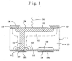
- the section shown in Figure 1 through an optoelectronic Sensor component as an example for the application of the inventive method for producing conductive Channels through a semiconducting base body of a semiconductor device shows a semiconductor device 1, the Base body made of silicon and a wide n-type Layer 100 (300 microns to 400 microns thick) includes the front Surface is a much thinner p-type Layer 101 (approx. 0.55 ⁇ m thick) extends. Between one is formed in the two semiconducting layers 100, 101 Space charge zone 102 (depletion zone), which acts as a barrier layer acts.
- the front of the component 1 is with an anti-reflection layer 108 and is provided by insulating layers 109 and 109 'structured, the z. B. from silicon dioxide can exist. Between the two insulating layers 109, 109 'extends the radiation-side surface area 104 by a surface of the p-type Layer 101 is formed. On surface area 104 incident electromagnetic radiation 200 passes through the p-type layer 101 into the space charge zone 102 and is largely absorbed there. This creates 102 electron-hole pairs in the space charge zone. The space charge field separates these pairs of supports; Electrons flow to the n-, holes to the p-side. To this photo stream that is a measure for the incident radiation power is to measure can, the component 1 must be in a suitable electrical Circuit can be integrated. Often such an electrical Circuit several photo elements and further semiconducting Components arranged together on a circuit board become.
- insulating layers 110 structured back surface 105 electrodes 106 and 107 with flat contact points 106a and 107a made of solderable material.
- the back surface 105 is thereby through a surface of the n-type Layer 100 itself formed.
- the terminal electrode 106 the n-type layer 100 is connected to a low-resistance, heavily doped region 103 of the semiconducting layer 100 arranged to minimize contact resistance.
- connection electrode 107 of the p-type layer 101 also on the rear surface 105 of the component 1 can be arranged, extends a cylindrical, semiconducting channel 111 of the p-type from the p-type Layer 101 to the rear surface 105 of the component 1.
- the p-type channel 111 preferably has one Diameter from 30 ⁇ m to 100 ⁇ m and is by means of thermomigration manufactured.
- the rear end of the passage 111 is also of surround an additional p-type region 112 which e.g. made by ion implantation or diffusion can be and the proper contacting of the p-type layer 101 over the cylindrical region 111 and enables the electrode 107.
- the extension of the additional p-type region 112 is selected such that it the near-surface portion of the cylindrical portion 111 so far encloses that in the manufacture of the cylindrical Area 111 occurring near the surface Disruptions in the electronic structure as far as possible be eliminated.
- the thickness of the additional p-type The range is of the order of 0.6 ⁇ m.
- Electrodes 106 and 107 of the n-type layer 100 and p-type layer 101 can the component 1 very easily on a circuit board connect and thereby into an electrical circuit integrate. To do this, only the electrodes 106 and 107 with their contact points 106a and 107a to designated ones Contact surfaces of the circuit board put on and through Soldering or ultrasonic welding can be attached. Additional Connecting elements, e.g. Solder bridges, between the Electrodes of the component 1 and the circuit board are unnecessary.
- the conductive channels in the semiconducting body Semiconductor component according to FIG. 1, for example generated with devices schematically in the figures 2a and 2c and in their entirety with a lamp field as Heat source are shown in Figure 2d. They are used for Inclusion of a semiconductor wafer, i.e. a board with a variety of semiconductor devices, the corresponding endowed and configured for their task and application are.
- a semiconductor wafer i.e. a board with a variety of semiconductor devices
- 2c and 2d Devices are also other devices with the same effect for holding semiconductor wafers and manufacturing conductive channels from one surface to the other of the arranged on the semiconductor wafer Semiconductor components possible.
- the longitudinal displacement of the frame 3a serves essentially a semiconductor wafer that can be inserted into the frame 3a 10 according to Figure 2b in the device for producing electrical conductive passages by means of thermomigration to insert or remove the semiconductor wafer.
- the edition 3a for the Semiconductor wafer 10 for example, only in the longitudinal direction Movable feed and removal of the semiconductor wafer be while the plate 60 and / or the cooling device 11th are adjustable in height so that the respective distance to Frame 3a can be changed.
- the plate 60 is part of a not shown Oven used to heat plate 60 by means of electrical Resistance heating, inductive heating device, electron beam heating, Microwave heating and the like. Heatable is. By appropriate energy input into the Edition 3 or the surface 3a facing away from the Plate 60 by injecting electrons, coupling in Radiation or the like can correspondingly energy into the plate 60 are entered, which in turn for an even Heat distribution over the entire area of the device provides. Instead of one plate 60, any other can appropriately suitable device for even heat distribution be used.
- the evenly heated plate 60 Due to the evenly heated plate 60 is a homogeneous heat distribution in the semiconductor wafer 10 facing surface ensured. Because there is any inhomogeneity the heat radiation emitted by the heat source images in the semiconductor wafer 10, is such a uniform Heat distribution particularly beneficial for both Production of electrically conductive passages through the entire area of the semiconductor wafer as well as to avoid bending the semiconductor wafer or the semiconductor wafer thereon located individual semiconductor elements.
- Heat radiation essentially on the arranged in the edition 3a Semiconductor wafer 10 is directed is the furnace or the plate 60 is thermally insulated by means of a vacuum, during the heat flow towards the in the Layer 3a located semiconductor wafer 10 by means of preferably an inert, good heat-conducting gas such as Hydrogen or helium, especially optimized by helium becomes.
- good heat-conducting gas such as Hydrogen or helium, especially optimized by helium becomes.
- the heated plate 60 for thermal insulation and Direction of heat radiation on the semiconductor wafer in the Vacuum is located, it is necessary for evaporation of particles that lead to contamination in the semiconductor wafer would lead to a correspondingly inactive material for select plate 60.
- Graphite with a boron nitride coating and a high-purity ceramic plate in question so that appropriate reactions suppressed and the process of thermomigration not through Impurities is affected.
- the semiconductor wafer inserted in the pad 3a 10 is a likewise inert gas, in particular helium, used for the process of thermomigration optimal temperature range at the bottom of the semiconductor wafer 10 set.
- the temperature on the surface of the semiconductor wafer 10 and on the lower surface the space in is preferably Height of the frame 3a divided so that both the gas pressure as well as the flow velocity in the space above the Frame 3a and below the frame 3a set separately can be.
- the possible separate temperature control creates the conditions for an optimal Course of the thermal migration process, so that electrical conductive passages in the disc-shaped semiconductor in minimal time without bending due to thermal stress of the semiconductor wafer.
- Figure 2c shows a schematic cross section through a alternative device in which instead of one between the Heat source 60 and the cooling device 11 arranged Frame 3a for receiving a semiconductor element 10, for example in the form of a silicon wafer Pins or webs 3c, which is on the cooling device 11 are supported or guided in the cooling device 11, so that the distance of the on the pins or webs 3c semiconductor wafers 10 lying on top of the cooling device 11 and be changed accordingly to heat source 6 can.
- a semiconductor element 10 for example in the form of a silicon wafer Pins or webs 3c
- the entered heat radiation W works on the surface of the semiconductor wafer facing the heat source 10, penetrates this and becomes a cooling device 11 forwarded.
- thermomigration The devices shown schematically in Figures 2a and 2c for the production of electrically conductive passages in disk-shaped semiconductors using thermomigration prove to be particularly energy-efficient and optimal regarding the thermal migration process.
- a device shown in detail in Figure 2d Production of passages through disc-shaped semiconductors Thermomigration consists of one in one Machine frame 20 arranged sample container 2, which itself from a movable sample stamp 3, a stationary one Recipient 4 and a likewise stationary outer jacket 5 composed.
- the sample stamp 3 is in the direction of Double arrow X on a guide rail 201 from one Loading position to one below a treatment position arranged position movable.
- a guide device 202 can the sample stamp 3 in the direction of Double arrow Z from below the treatment position located position in the treatment position via a Lifting height H can be moved.
- a cradle 203 for gas supply lines, cooling lines, measuring cables and The like. is with the carriage receiving the sample stamp 3 204 connected.
- the top of the recipient 4 is in a light exit aperture 14 stored, the sample container 2 below centered a heat source 6, which preferably consists of two crossed Halogen lamp fields 61, 62 there.
- the crossed Halogen lamp fields 61, 62 have a large number individually controllable halogen lamps so that a homogeneous Heat radiation on the surface facing the heat source 6 of the semiconductor wafer 10 is ensured.
- By the adjustable temperature curve over the semiconductor wafer surface there is a possibility of bringing the temperature to the edge of the Raising the wafer surface so that an individual Temperature profile set over the wafer surface can be.
- This adjustability of the lighting mood i.e. the power distribution for temperature homogenization, ensures equal conditions over the entire surface of the semiconductor wafer, so that by means of a special Temperature measuring method optimal conditions for thermomigration can be adjusted.
- a mirror reflector 13 is arranged above the heat source 6, which together with the heat source 6 and the Light exit aperture 14 via a bracket 15 with the Machine frame 20 is connected.
- One of a 3-point lifting plate 37 and a guide lifting plate 38 assembled lifting plate seals the sample stamp 3 down to the bottom, with the 3-point lifting plate 37 a uniform system for gas-tight closure of the sample stamp 3 has.
- FIG. 3 shows a longitudinal section through the sample container 2 with a pyrometer measuring head 7 arranged therein.
- the sample container 2 is made up of the outer, by means of a cooling tube 11 cooled outer jacket 5 and with this connected via a seal 17 or Sample receiving cylinder 4 and the movable sample stamp 3 together.
- the recipient 4 and the outer jacket 5 are via a further seal 18 with a fastening ring 19 connected and via a cover-side flange 50 of the outer jacket 5 on the light exit diaphragm 14 according to FIG. 2d attached.
- the recipient 4 has a radiation passage area on its upper side 40 through which the from the halogen lamp fields 61, 62 of the heat source 6 emitted radiation onto a sample head 30 at the top of the sample stamp 3 arrives. There is an unspecified one on the sample head 30 Sample holder for storing the material to be processed Semiconductor wafers 10 are provided. With a three-point tip bearing becomes an equidistant storage of the semiconductor wafer 10 to the surface of the probe head 30 with a Accuracy of 200 to 300 ⁇ m guaranteed.
- the radiation passage area 40 of the recipient 4 has great optical homogeneity and at a given wavelength has a high transmissibility and exists preferably made of quartz or sapphire.
- a pyrometer measuring head 7 Centrally within a sample cylinder 35 of the sample stamp 3 is a pyrometer measuring head 7 is arranged, which a temperature measuring and gas channel 9 and one in the temperature measuring and gas channel 9 located measurement window 12 to the Sample head 30 or the surface facing the sample holder of the semiconductor wafer 10 is directed.
- the pyrometer measuring head 7 with a preferred wavelength of 2.2 microns a finely adjustable focus cone that only one detected a small spot on the semiconductor wafer 10 so that no significant disturbance due to the temperature measurement between the semiconductor wafer 10 and the probe head 30 occurs.
- This measurement spot is representative of the temperature on the entire semiconductor wafer 10 since - as above was carried out in connection with Figure 2d - the power distribution across the surface of the semiconductor wafer 10 by means of the individually controllable halogen lamps of the crossed Halogen lamp field 61, 62 of the heat source 6 adjustable is.
- the measurement window 12 preferably consists of sapphire (Al 2 O 3 ), which is preferred to a quartz window, since it is open into the wide infrared wave range.
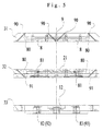
- the sample head 30 has three head planes 31, 32, 33, of which the sample is taken with the first Probe head level 31 is connected.
- the first probe level 31 of the sample head 30 has the central temperature measurement Gas channel 9 and several radially distributed, diagonal gas channels 90 guided through the first probe head plane 31 through which a highly thermally conductive gas such as helium or Hydrogen passed and through the nozzle-shaped openings of channels 9 and 90 emerges and under the semiconductor wafer 10 streams.
- the gas supply serves to keep the process room clean, the flow is preferably 0.5 to 50 mbar / l gas flow is set so that the semiconductor wafer 10 is not raised by the gas flow and none Inhomogeneities occur.
- the removal of the process gas takes place via an opening 95 in the base area of the sample cylinder 35th
- the second probe head plane 32 of the probe head 30 is diagonal Gas channels 91, the central temperature measuring and gas channel 9 and cooling water channels 81, which form cooling elements 8 lead to the enlargement of the heat-absorbing surface Recesses 80 included.
- the connection between the first probe head level 31 and the second probe head level 32 is done by means of liquid-tight sealing rings as well gastight outer rings that fit into corresponding openings the mutually facing surfaces of the first and second Sample head plane 31, 32 of the sample head 30 are arranged.
- the third probe head plane 33 of the probe head 30 has a coolant inlet 82 and a coolant outlet 83 or when the third probe head plane 33 rotates by 90 ° a corresponding gas inlet 92 and gas outlet 93 for the process gas.
- Centrally in the third probe head plane 33 of the sample head 30 is embedded in the measuring window 12, which is located in the optical temperature measuring channel 9.
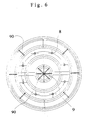
- Probe head level 31 illustrates the arrangement of the gas and Coolant channels and the measuring opening 9 for detection the wafer temperature.
- the three probe head levels 31 to 33 are preferably made from pure aluminum.
- the one laid in a spiral around the outer jacket 5 in FIG Cooling tube 11a causes the sample container 2 to cool down the top facing the heat source 6 to the base side Sealing area so that the functionality of the Seals between the outer jacket 5, the recipient 4th and the sample stamp 3 is guaranteed.
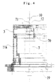
- FIG. 4 Another embodiment of the cooling is in FIG. 4 shown, in which a cooling cylinder 11a inside the Sample stamp 3 is arranged so that there is a cavity to hold coolant in a hollow cylindrical shape inside of the sample stamp 3 extends.
- a cooling cylinder 11a inside the Sample stamp 3 is arranged so that there is a cavity to hold coolant in a hollow cylindrical shape inside of the sample stamp 3 extends.
- Another variant is both external cooling coil cooling 3 with an internal cooling cylinder cooling according to Figure 4 to combine.
- the pyrometer measuring head 7 is by means of a pyrometer flange 70 fixed to the sample stamp 3 and can accordingly be adjusted.
- the focus cone 71 of the pyrometer measuring head 7 is directed towards the surface of the semiconductor wafer 10, that there is a small measuring spot in the middle of the semiconductor wafer 10 shows where no semiconductor device is arranged is.
- thermal migration device With the thermal migration device described above is a highly precise controllable heat transfer through the semiconductor wafer 10 from the crossed halogen lamp arrays 61, 62 of the heat source 6 facing back of the semiconductor wafer 10 to that of the cooled probe head 30 facing top of the semiconductor wafer 10 guaranteed.
- adjustable temperature difference of approximately 2 ° C up to 10 ° C with a thickness of the semiconductor wafer of approx. 300 ⁇ m migrates to the cooler surface of the semiconductor wafer 10 or arranged on the semiconductor wafer
- electrically conductive (Aluminum) droplets with a thickness of approx. 2 to 3 ⁇ m to the opposite, warmer surface of the semiconductor wafer 10 and thus brings about the desired conductive Connection between the opposite surfaces of the Semiconductor wafers or the semiconductor components on the provided connection points.
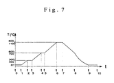
- Figure 7 illustrates an embodiment of the invention Process for making electrical, conductive Connections between the opposite surfaces a semiconductor wafer by means of thermomigration, the The method shown in FIG. 7 can be modified in various ways is.
- the sample stamp 3 with the sample head 30 is moved out of the recipient 4 or the outer jacket 5 in the direction of the arrow Z according to FIG. 2d and moved to the loading point.
- the sample stamp 3 is first moved in the X direction and then in the Z direction according to FIG. 2d into the treatment position, that is to say it is moved into the recipient 4 and the system is closed.
- the sample stamp 3 is evacuated and helium is flushed into the sample stamp 3 in a flushing phase.
- the admission of cooling water into the sample stamp 3 ends the preparation phase at time t 1 .
- the sample is heated by switching on the heat source 6 with a temperature increase of approx. 30 ° C./second to time t 2 to a temperature of approx. 300 ° C. to 400 ° C. At this temperature, the sample atmosphere is cleaned again (helium flushing) over a period of approx. 1 min. until time t 3 . Subsequently, the sample is further heated up to a temperature of approximately 600 ° C. to 670 ° C. (time t 4 ), at which the aluminum droplet applied to the surface of the semiconductor wafer 10 reacts with the semiconducting base body by droplet formation (time t 5 ). The sample is then further heated to a working temperature of approximately 800 ° C. to 1100 ° C., at which the migration process takes place, ie the aluminum droplet migrates through the semiconducting base body of the semiconductor components arranged on the semiconductor wafer.
- the migration rate is proportional to the temperature gradient and the working temperature and determines the duration of the thermomigration (t 6 to t 7 ).
- the sample temperature is ramped down with a temperature decrease of approx. 30 ° C per second.
- time t 8 the sample is left to cool freely, so that the sample temperature in a period of about 2 to 3 min. (Time t 9 ) is shut down.
Landscapes
- Testing Or Measuring Of Semiconductors Or The Like (AREA)
- Internal Circuitry In Semiconductor Integrated Circuit Devices (AREA)
- Chemically Coating (AREA)
- Electrodes Of Semiconductors (AREA)
Description
- Figur 1 -
- einen Querschnitt durch ein optoelektronisches Sensor-Bauelement mit einem zylindrischen, halbleitenden Verbindungskanal von der Vorder- zur Rückseite des Halbleiter-Bauelements;
- Figur 2a -
- eine schematische Prinzipdarstellung einer Vorrichtung zur Herstellung elektrisch leitfähiger Durchgänge in einem scheibenförmigen Halbleiter mittels Thermomigration;
- Figur 2b -
- eine schematische Darstellung eines Halbleiter-Wafers;
- Figur 2c -
- einen Querschnitt durch eine Vorrichtung gemäß Figur 2a mit Stiften oder Stegen zur Abstützung eines Halbleiter-Wafers;
- Figur 2d -
- eine Seitenansicht einer Vorrichtung zum Erzeugen von Durchgangskanälen in einem Halbleiter-Wafer mittels eines Lampenfeldes als Wärmequelle;
- Figur 3 -
- einen Längsschnitt durch einen Probenbehälter mit Außenkühlung zur Aufnahme eines Halbleiter-Wafers ;
- Figur 4 -
- einen schematischen Längsschnitt durch einen Teil eines Probenbehälters mit Innenkühlung;
- Figur 5 -
- Längsschnitte durch die einzelnen Ebenen eines Probenkopfes;
- Figur 6 -
- eine Draufsicht auf die erste Ebene des Probenkopfes und
- Figur 7 -
- ein schematisches Themperatur-Zeitdiagramm des erfindungsgemäßen Thermomigrationsprozesses.
a1 = 0,3 mm.
a2 = 0,2 bis 0,5 mm
während im Bereich oberhalb des Halbleiter-Wafers ein Gasdruck von ca. 0,1 bis 30 mbar eingestellt wird.
| 1 | Halbleiter-Bauelement | 100 | Halbleiter-Grundkörper (n-leitende Schicht) |
| 101 | Halbleiter-Grundkörper (p-leitende Schicht) | ||
| 102 | Raumladungszone | ||
| 103 | niederohmiger, stark dotierter Bereich | ||
| 104 | Oberflächenbereich | ||
| 105 | rückseitige Oberfläche | ||
| 106 | Elektrode | ||
| 106a | Kontaktstelle | ||
| 107 | Elektrode | ||
| 107a | Kontaktstelle | ||
| 108 | Antireflexionsschicht | ||
| 109 | isolierende Schicht | ||
| 110 | isolierende Schicht | ||
| 111 | (halb)leitender Kanal | ||
| 2 | Probenbehälter | ||
| 3 | Auflage | 3a | Rahmen |
| 3b | Probenstempel | ||
| 3c | Stege, Stifte | ||
| 30 | Probenkopf | ||
| 31 | 1. Probenkopfebene | ||
| 32 | 2. Probenkopfebene | ||
| 33 | 3. Probenkopfebene | ||
| 35 | Probenzylinder | ||
| 36 | Probenflansch | ||
| 37 | 3-Punkt-Hubteller | ||
| 38 | Führungs-Hubteller | ||
| 4 | Rezipient | 40 | Strahlendurchtrittsfläche |
| 41 | Quarzzylinder | ||
| 5 | Außenmantel | 50 | Außenmantel-Flansch |
| 6 | Wärmequelle | 60 | Platte |
| 61 | 1. Halogenlampenebene | ||
| 62 | 2. Halogenlampenebene | ||
| 7 | Pyrometer-Meßkopf | 70 | Pyrometerflansch |
| 71 | Fokuskegel | ||
| 8 | Flüssigkeitskühlung | 80 | Kühlkammer |
| 81 | Kühlkanal | ||
| 82 | Kühlflüssigkeits-Einlaß | ||
| 83 | Kühlflüssigkeits-Auslaß | ||
| 9 | Temperaturmeß- und Gaskanal | 90 | Gasaustrittsdüsen |
| 91 | Gaskanäle | ||
| 92 | Gaseinlaß | ||
| 93 | Gasauslaß | ||
| 95 | Gasabfuhr | ||
| 10 | Halbleiter(-Wafer) | ||
| 11 | Kühleinrichtung | 11a | Kühlrohr |
| 11b | Kühlzylinder | ||
| 12 | Meßfenster | ||
| 13 | Spiegelreflektor | ||
| 14 | Lichtaustrittsblende | ||
| 15 | Halterung | ||
| 16 | Gasdichtung | ||
| 17 | Dichtung | ||
| 18 | Dichtung | ||
| 19 | Befestigungsring | ||
| 20 | Maschinenrahmen | 201 | Horizontalführung |
| 202 | Vertikalführung | ||
| 203 | Leitungsaufnahme | ||
| 21 | Dichtungsringe | ||
| 25 | Gestell |
Claims (37)
- Verfahren zur Herstellung elektrisch leitfähiger Durchgänge in einem scheibenförmigen Halbleiter mittels Thermomigration durch Erzeugen eines Temperaturgradienten zwischen zwei entgegengesetzten Oberflächen des Halbleiters (10), wobei die erste Oberfläche gleichmäßig über die Oberfläche verteilt bis auf eine Arbeitstemperatur des Thermomigrationsprozesses von 800°C bis 1100°C erwärmt und anschließend bis auf eine Entnahmetemperatur abgesenkt wird und auf die zweite Oberfläche ein leitfähiger Dotierungsstoff aufgebracht und die zweite Oberfläche gleichmäßig über die Oberfläche verteilt gekühlt wird,
dadurch gekennzeichnet, daß die erste Oberfläche einen ersten Abstand (a1) zu einer Wärmequelle (6) und die zweite Oberfläche einen zweiten Abstand (a2) zu einer Kühleinrichtung (11) aufweist und die Gesamtleistung des Wärmeeintrags in den Halbleiter (10) und/oder die Leistungsverteilung des Wärmeeintrags über die zu erwärmende Oberfläche des Halbleiters (10) in Abhängigkeit von der an mindestens einem Temperatur-Meßpunkt auf dem Halbleiter (10) gemessenen Temperatur durch Veränderung des ersten und zweiten Abstandes (al, a2) eingestellt wird. - Verfahren nach Anspruch 1, dadurch gekennzeichnet, daß der Halbleiter (10) in einem geschlossenen, mit einem gut wärmeleitenden, inertgasgefüllten System (2, 3) angeordnet wird.
- Verfahren nach Anspruch 2, dadurch gekennzeichnet, daß das Inertgas aus Wasserstoff oder Helium besteht.
- Verfahren nach mindestens einem der vorangehenden Ansprüche, dadurch gekennzeichnet, daß der Halbleiter (10) senkrecht zur der Ebene zwischen Wärmequelle und Kühleinrichtung zu bewegen ist.
- Verfahren nach mindestens einem der vorangehenden Ansprüche, dadurch gekennzeichnet, daß die Oberflächen des Halbleiters (10) in voneinander getrennten Räumen angeordnet werden.
- Verfahren nach mindestens einem der vorangehenden Ansprüche, dadurch gekennzeichnet, daß die Wärmestrahlung im wesentlichen senkrecht auf die zu erwärmende Oberfläche des Halbleiters (10) auftrifft.
- Verfahren nach mindestens einem der vorangehenden Ansprüche, dadurch gekennzeichnet, daß der Halbleiter (10) auf einem in mindestens einer Ebene beweglichen Probenstempel (3) angeordnet wird, der zwischen einer Beschickungs- und einer Bestrahlungsposition bewegt wird.
- Verfahren nach mindestens einem der vorangehenden Ansprüche, dadurch gekennzeichnet, daß die Temperatur des Halbleiters (10) mit einer pyrometrischen Meßeinrichtung (7) über einen optischen Meßkanal (9) berührungsfrei gemessen wird.
- Verfahren nach mindestens einem der vorangehenden Ansprüche, dadurch gekennzeichnet, daß die Aufheizung des Halbleiters (10) mit einem Temperaturanstieg kleiner oder gleich 30 K/Sekunde erfolgt, anschließend die Temperatur konstant gehalten wird, bis der Thermomigrationsprozess abgeschlossen ist, in einer ersten Abkühlphase mit abnehmender Wärmestrahlung abgekühlt und anschließend über eine vorgegebene Zeitspanne in freier Abkühlung bis zur Entnahmetemperatur abgekühlt wird.
- Verfahren nach Anspruch 9, dadurch gekennzeichnet, daß die Aufheizung und Abkühlung des Halbleiters (10) nach einer Rampenfunktion erfolgt.
- Verfahren nach mindestens einem der vorangehenden Ansprüche, dadurch gekennzeichnet, daß der Halbleiter (10) bis zu einer ersten vorgegebenen Temperatur von 300°C bis 400°C aufgeheizt wird, daß nach dem Erreichen dieser Temperatur des Halbleiters (10) der den Halbleiter (10) umgebende Raum über eine vorgegebene Zeitspanne gereinigt wird, daß der Halbleiter (10) auf eine zweite vorgegebene Temperatur von ca. 600°C bis 700°C weiter erhitzt wird, bei der der leitfähige Dotierungsstoff mit dem halbleitenden Grundkörper des Halbleiters durch Tröpfchenbildung reagiert, und daß anschließend auf die Arbeitstemperatur des Migrationsprozesses von ca. 900°C bis 1100°C aufgeheizt wird, daß nach Beendigung des Thermomigrationsprozesses die Temperatur des Halbleiters (10) bis zu einer dritten vorgegebenen Temperatur von ca. 650°C abgesenkt und anschließend der Halbleiter (10) über eine Zeitspanne von ca. zwei bis drei Minuten auf eine vorgegebene Entnahmetemperatur abgekühlt wird.
- Verfahren nach mindestens einem der Ansprüche 7 bis 11, dadurch gekennzeichnet, daß der Probenstempel (3) in eine Entnahme- und Beschickungsposition gefahren und zur Aufnahme des Halbleiters (10) geöffnet wird, daß der Probenstempel (3) nach dem Beschicken des Halbleiters (10) in eine geschlossene Position gebracht und der Probenstempel (3) evakuiert und mit einem Inertgas gespült wird, daß eine Kühlflüssigkeit in den Probenstempel (3) eingelassen und der Halbleiter (10) nach dem vorgegebenen Programm aufgeheizt und abgekühlt wird, daß der Probenstempel (3) erneut in die Entnahme- und Beschickungsposition gefahren und der Halbleiter (10) entnommen und in ein mit Stickstoff umspültes Magazin angeordnet wird.
- Vorrichtung zur Herstellung elektrisch leitfähiger Durchgänge in einem scheibenförmigen Halbleiter mittels Thermomigration durch Erzeugen eines Temperaturgradienten zwischen zwei entgegengesetzten Oberflächen des Halbleiters, von denen eine Oberfläche einer Wärmequelle (6) und die andere Oberfläche einer Kühleinrichtung (11) zugewandt ist, und Aufbringen eines leitfähigen Dotierungsstoffes auf die der Wärmequelle (6) zugewandten Oberfläche mit einer zwischen der Wärmequelle (6) und der Kühleinrichtung (11) angeordnete Auflage zur Aufnahme des Halbleiters, wobei die Wärmequelle (6) eine homogene Wärmestrahlung an die ihr zugewandte Oberfläche des Halbleiters (10) abgibt,
dadurch gekennzeichnet daß die Vorrichtung einen Pyrometermeßkopf (7) zur Messung der Oberflächentemperatur des Halbleiters (10) aufweist und der Abstand zwischen der Auflage (3) und der Wärmequelle (6) und/oder zwischen der Auflage (3) und der Kühleinrichtung (11) in Abhängigkeit von der gemessenen Oberflächentemperatur veränderbar ist. - Vorrichtung nach Anspruch 13, dadurch gekennzeichnet, daß der Raum zwischen der Wärmequelle (6) und der Kühleinrichtung (11) gekapselt und mit einem inerten, gut wärmeleitenden Gas gefüllt ist.
- Vorrichtung nach Anspruch 14, dadurch gekennzeichnet, daß es sich bei dem Gas um Wasserstoff oder Helium handelt.
- Vorrichtung nach Anspruch 14 oder 15, dadurch gekennzeichnet, daß der Raum' in der Ebene der Auflage (3) unterteilt ist.
- Vorrichtung nach einem der Ansprüche 14 bis 16, dadurch gekennzeichnet, daß der Gasdruck und/oder die Gasströmung in dem Raum bzw. den Räumen veränderbar ist.
- Vorrichtung nach einem der vorangehenden Ansprüche 13 bis 17, dadurch gekennzeichnet, daß die Wärmequelle (6) aus einem direkt oder indirekt beheizten Ofen besteht.
- Vorrichtung nach Anspruch 18, dadurch gekennzeichnet, daß der Ofen eine im wesentlichen der Fläche der Auflage (3) entsprechende Platte (60) aufweist, die mittels elektrischer Widerstandsheizung, induktiver Heizung, Elektronenstrahl-Heizung oder mittels Mikrowellenheizung aufheizbar ist.
- Vorrichtung nach Anspruch 19, dadurch gekennzeichnet, daß die Platte (60) aus einem pyrolytisch mit Bornitrid versiegeltem Graphitmaterial besteht.
- Vorrichtung nach Anspruch 19, dadurch gekennzeichnet, daß die Platte (60) aus Reinstkeramik besteht.
- Vorrichtung nach Anspruch 13, dadurch gekennzeichnet, daß die Wärmequelle (6) aus einem Halogenlampenfeld (61 bzw. 62) besteht, das sich zumindest über die Fläche des Halbleiters (10) erstreckt.
- Vorrichtung nach Anspruch 13 oder 22, dadurch gekennzeichnet, daß die Wärmequelle (6) aus in zwei Ebenen angeordneten, gekreuzten Halogenlampenfeldern (61, 62) besteht.
- Vorrichtung nach mindestens einem der vorangehenden Ansprüche 13 bis 23, dadurch gekennzeichnet, daß ein Spiegelreflektor (13) auf der der Auflage (3) gegenüberliegenden Seite der Wärmequelle (6) angeordnet ist.
- Vorrichtung nach mindestens einem der vorangehenden Ansprüche 13 bis 24, dadurch gekennzeichnet, daß die Auflage (3) aus einem Rahmen (3a) besteht, der in einer Ebene parallel zur Längserstreckung der Wärmequelle (6) beweglich ist.
- Vorrichtung nach mindestens einem der vorangehenden Ansprüche 13 bis 24, dadurch gekennzeichnet, daß die Auflage (3) aus mit der Kühleinrichtung (8) verbundenen Stiften oder Stegen (3c) besteht, die die der Kühleinrichtung (8) zugewandte Oberfläche des Halbleiters (10) punkt- oder linienförmig abstützen.
- Vorrichtung nach mindestens einem der vorangehenden Ansprüche 13 bis 26, dadurch gekennzeichnet, daß die Auflage (3) aus einem mit der Kühleinrichtung (11, 11a) verbundenen Probenstempel (3) besteht.
- Vorrichtung nach Anspruch 27, dadurch gekennzeichnet, daß der Probenstempel (3) aus einem Probenzylinder (35), einem die Deckfläche des Probenzylinders (35) bildenden, den Halbleiter (10) aufnehmenden Probenkopf (30), einem an der Unterseite des Probenzylinders (35) nach außen abstehenden Probenflansch (36) und einem den Probenzylinder (35) zur Unterseite gasdicht abschließenden Hubteller (37, 38) besteht.
- Vorrichtung nach Anspruch 28, dadurch gekennzeichnet; daß der Probenstempel (3) in axialer Richtung (Z-Richtung) in einen Rezipienten (4), der aus einer der Wärmequelle (6) zugewandten Strahlendurchtrittsfläche (40) und einem Quarzzylinder (41) besteht, ein- und ausfahrbar ist.
- Vorrichtung nach Anspruch 29, dadurch gekennzeichnet, daß der Rezipient (4) von einem zylinderförmigen Außenmantel (5) umgeben ist, und daß der zylinderförmige Außenmantel (5) gekühlt und/oder innerhalb des Probenstempels (3) ein Kühlzylinder (11a) angeordnet ist.
- Vorrichtung nach mindestens einem der Ansprüche 28 bis 30, dadurch gekennzeichnet, daß der Pyrometermeßkopf (7) zentrisch innerhalb des Probenzylinders (35) des Probenstempels (3) angeordnet ist und über einen Temperaturmeß- und Gaskanal (9) sowie ein im Temperaturmeß- und Gaskanal (9) befindliches Meßfenster (12) auf die dem Probenkopf (30) zugewandte Oberfläche des Halbleiters (10) gerichtet ist.
- Vorrichtung nach Anspruch 31, dadurch gekennzeichnet, daß der Pyrometer-Meßkopf (7) einen fein einstellbaren Fokuskegel aufweist.
- Vorrichtung nach Anspruch 31 oder 32, dadurch gekennzeichnet, daß der Pyrometer-Meßkopf (7) mit einer Wellenlänge von 2,2 µm arbeitet.
- Vorrichtung nach Anspruch 31, 32 oder 33, dadurch gekennzeichnet, daß der Pyrometer-Meßkopf (7) mittels eines Pyrometerflansches (70) am Probenstempel (3) fixiert und justiert ist und daß der Fokuskegel (71) des Pyrometer-Meßkopfes (7) so auf die Oberfläche des Halbleiters (10) gerichtet ist, daß sich ein kleiner Meßfleck in der Mitte des Halbleiters (10) ergibt.
- Vorrichtung nach Anspruch 34, dadurch gekennzeichnet, daß das Meßfenster (12) aus Saphir (Al2O3) besteht.
- Vorrichtung nach mindestens einem der vorangehenden Ansprüche 13 bis 35', dadurch gekennzeichnet, daß der Probenkopf (30) drei Probenkopfebenen (31, 32, 33) ,aufweist, von denen die Aufnahme des Halbleiters (10) mit der ersten Probenkopfebene (31) verbunden ist, die den zentralen Temperaturmeß- und Gaskanal (9) sowie mehrere radial verteilte, diagonal durch die erste Probenkopfebene (31) geführte Gaskanäle (90) aufweist, durch die ein gut wärmeleitendes Gas geleitet und über düsenförmigen Öffnungen der Kanäle (9 bzw. 90) austritt, unter den Halbleiter (10) strömt und über eine Öffnung (95) im Sockelbereich des Probenzylinders (35) angeführt wird,
daß die zweite Probenkopfebene (32) des Probenkopfes (30) diagonale Gaskanäle (91), den zentralen Temperaturmeß- und Gaskanal (9) und Kühlwasserkanäle (81) aufweist, die zu Kühlelementen (8) führen,
und daß die dritte Probenkopfebene (33) des Probenkopfes (30) einen Kühlflüssigkeitseinlaß (82) und einen Kühlflüssigkeitsauslaß (83) sowie einen Gaseinlaß (92) und Gasauslaß (93) für das Prozeßgas aufweist, daß zentrisch in die dritte Probenkopfebene (33) des Probenkopfes (30) das sich im optischen Temperaturmeßkanal (9) befindende Meßfenster (12) eingelassen ist. - Vorrichtung nach Anspruch 36, dadurch gekennzeichnet, daß die drei Probenkopfebenen (31 bis 33) aus Reinstaluminium bestehen.
Applications Claiming Priority (3)
| Application Number | Priority Date | Filing Date | Title |
|---|---|---|---|
| DE19727693 | 1997-06-20 | ||
| DE19727693A DE19727693A1 (de) | 1997-06-20 | 1997-06-20 | Verfahren und Vorrichtung zur Herstellung elektrisch leitfähiger Durchgänge in Halbleiter-Bauelementen |
| PCT/DE1998/001768 WO1998059098A2 (de) | 1997-06-20 | 1998-06-22 | Verfahren und vorrichtung zur herstellung elektrisch leitfähiger durchgänge in halbleiter-bauelementen |
Publications (2)
| Publication Number | Publication Date |
|---|---|
| EP0991797A2 EP0991797A2 (de) | 2000-04-12 |
| EP0991797B1 true EP0991797B1 (de) | 2002-07-24 |
Family
ID=7834047
Family Applications (1)
| Application Number | Title | Priority Date | Filing Date |
|---|---|---|---|
| EP98943631A Expired - Lifetime EP0991797B1 (de) | 1997-06-20 | 1998-06-22 | Verfahren und vorrichtung zur herstellung elektrisch leitfähiger durchgänge in halbleiter-bauelementen |
Country Status (8)
| Country | Link |
|---|---|
| US (1) | US6300256B1 (de) |
| EP (1) | EP0991797B1 (de) |
| JP (1) | JP2000512438A (de) |
| KR (1) | KR100348439B1 (de) |
| CN (1) | CN1261410A (de) |
| AT (1) | ATE221146T1 (de) |
| DE (2) | DE19727693A1 (de) |
| WO (1) | WO1998059098A2 (de) |
Families Citing this family (6)
| Publication number | Priority date | Publication date | Assignee | Title |
|---|---|---|---|---|
| DE19929307C1 (de) * | 1999-06-25 | 2000-11-09 | Siemens Ag | Verfahren zur Herstellung einer strukturierten Schicht und dadurch hergestellte Elektrode |
| US20020063117A1 (en) * | 2000-04-19 | 2002-05-30 | Church Kenneth H. | Laser sintering of materials and a thermal barrier for protecting a substrate |
| DE10302653A1 (de) * | 2003-01-20 | 2004-08-19 | Htm Reetz Gmbh | Vorrichtung zur Thermomigration |
| JP5530856B2 (ja) * | 2010-08-18 | 2014-06-25 | 信越半導体株式会社 | ウエーハの熱処理方法及びシリコンウエーハの製造方法並びに熱処理装置 |
| CN102420201B (zh) * | 2011-11-16 | 2013-05-22 | 华中科技大学 | 硅通孔结构及其制造方法 |
| CN121141769B (zh) * | 2025-09-10 | 2026-05-12 | 延边大学 | 一种高压-温度耦合场下半导体材料电学性能的调控方法 |
Family Cites Families (10)
| Publication number | Priority date | Publication date | Assignee | Title |
|---|---|---|---|---|
| US4081293A (en) * | 1976-10-18 | 1978-03-28 | General Electric Company | Uniform thermomigration utilizing sample movement |
| US4101759A (en) * | 1976-10-26 | 1978-07-18 | General Electric Company | Semiconductor body heater |
| US4097226A (en) * | 1976-10-26 | 1978-06-27 | General Electric Company | Furnace for practising temperature gradient zone melting |
| US4157564A (en) * | 1976-11-19 | 1979-06-05 | General Electric Company | Deep diode devices |
| US4221956A (en) * | 1978-06-21 | 1980-09-09 | General Electric Company | Apparatus for practising temperature gradient zone melting |
| US4224504A (en) * | 1978-06-21 | 1980-09-23 | General Electric Company | Apparatus for practicing temperature gradient zone melting |
| US4159215A (en) * | 1978-09-21 | 1979-06-26 | General Electric Company | Droplet migration doping using reactive carriers and dopants |
| WO1983003710A1 (en) * | 1982-04-09 | 1983-10-27 | Hughes Aircraft Co | Temperature gradient zone melting process and apparatus |
| DE3276036D1 (en) * | 1982-08-24 | 1987-05-14 | Bbc Brown Boveri & Cie | Process for the thermomigration of liquid phases, and apparatus for carrying out this process |
| US5970214A (en) * | 1998-05-14 | 1999-10-19 | Ag Associates | Heating device for semiconductor wafers |
-
1997
- 1997-06-20 DE DE19727693A patent/DE19727693A1/de not_active Withdrawn
-
1998
- 1998-06-22 US US09/446,408 patent/US6300256B1/en not_active Expired - Fee Related
- 1998-06-22 WO PCT/DE1998/001768 patent/WO1998059098A2/de not_active Ceased
- 1998-06-22 AT AT98943631T patent/ATE221146T1/de not_active IP Right Cessation
- 1998-06-22 KR KR1019997012071A patent/KR100348439B1/ko not_active Expired - Fee Related
- 1998-06-22 EP EP98943631A patent/EP0991797B1/de not_active Expired - Lifetime
- 1998-06-22 CN CN98806425A patent/CN1261410A/zh active Pending
- 1998-06-22 DE DE59804904T patent/DE59804904D1/de not_active Expired - Fee Related
- 1998-06-22 JP JP11503593A patent/JP2000512438A/ja active Pending
Also Published As
| Publication number | Publication date |
|---|---|
| DE59804904D1 (de) | 2002-08-29 |
| CN1261410A (zh) | 2000-07-26 |
| WO1998059098A3 (de) | 1999-03-18 |
| EP0991797A2 (de) | 2000-04-12 |
| ATE221146T1 (de) | 2002-08-15 |
| DE19727693A1 (de) | 1998-12-24 |
| US6300256B1 (en) | 2001-10-09 |
| JP2000512438A (ja) | 2000-09-19 |
| KR20010014041A (ko) | 2001-02-26 |
| KR100348439B1 (ko) | 2002-08-10 |
| WO1998059098A2 (de) | 1998-12-30 |
Similar Documents
| Publication | Publication Date | Title |
|---|---|---|
| DE2945177C2 (de) | ||
| DE102007035166B4 (de) | Hochtemperatur-Verdampferzelle mit parallel geschalteten Heizbereichen, Verfahren zu deren Betrieb und deren Verwendung in Beschichtungsanlagen | |
| EP1540717B1 (de) | Verfahren zum oxidieren einer schicht und zugehörige aufnahmevorrichtungen für ein substrat | |
| DE69118513T2 (de) | Vorrichtung zum erwärmen von halbleiterscheiben oder -substraten | |
| DE10296662T5 (de) | Systeme und Verfahren zum epitaxialen Aufwachsen von Filmen auf ein Halbleitersubstrat | |
| DE2354523C3 (de) | Verfahren zur Erzeugung von elektrisch isolierenden Sperrbereichen in Halbleitermaterial | |
| EP1277238B1 (de) | Vorrichtung und Verfahren zum gleichzeitigen Temperieren mehrerer Prozessiergüter | |
| EP0991797A2 (de) | Verfahren und vorrichtung zur herstellung elektrisch leitfähiger durchgänge in halbleiter-bauelementen | |
| DE68920414T2 (de) | Herstellungsverfahren von Sonnenzellen. | |
| DE2536174C3 (de) | Verfahren zum Herstellen von polykristallinen Siliciumschichten für Halbleiterbauelemente | |
| WO2000014310A1 (de) | Vorrichtung zum herstellen und bearbeiten von halbleitersubstraten | |
| DE10325602B3 (de) | Verfahren zur temperaturgeregelten Prozessierung von Substraten | |
| DE102016111234B4 (de) | Vorrichtung für die thermische Behandlung eines Substrats sowie Trägerhorde und Substrat-Trägerelement dafür | |
| DE102010011156B4 (de) | Vorrichtung zur thermischen Behandlung von Halbleitersubstraten | |
| EP1590510B1 (de) | Vorrichtung zur herstellung elektrisch leitfähiger durchgänge in einem halbleiterwafer mittels thermomigration | |
| DE102005025935B4 (de) | Hochtemperatur-Verdampferzelle und Verfahren zur Verdampfung hochschmelzender Materialien | |
| DE102008030679B4 (de) | Vorrichtung zur Diffusionsbehandlung von Werkstücken | |
| DE2621418C2 (de) | Verfahren und Vorrichtung zum Dotieren von Halbleiterplättchen | |
| DE69729091T2 (de) | In-situ-Diffusion von Dotierstoffen bei dendritisch vernetztem Wachstum eines kristallinen Siliziumbandes | |
| DE2743856C2 (de) | Vorrichtung zum Abscheiden von Halbleitermaterial | |
| WO2018234389A1 (de) | Beheizbarer waferträger und bearbeitungsverfahren | |
| WO1989010632A1 (fr) | Procede de fabrication de cellules solaires et four a miroir pour appliquer ledit procede | |
| US4157564A (en) | Deep diode devices | |
| DD234748A1 (de) | Vorrichtung zum durchfuehren thermischer prozesse in der halbleiterfertigung | |
| DE2226728C2 (de) | Einrichtung zum Züchten von Kristallen nach dem Flammenschmelzverfahren |
Legal Events
| Date | Code | Title | Description |
|---|---|---|---|
| PUAI | Public reference made under article 153(3) epc to a published international application that has entered the european phase |
Free format text: ORIGINAL CODE: 0009012 |
|
| 17P | Request for examination filed |
Effective date: 20000105 |
|
| AK | Designated contracting states |
Kind code of ref document: A2 Designated state(s): AT CH DE ES FR GB IT LI NL SE |
|
| 17Q | First examination report despatched |
Effective date: 20010219 |
|
| GRAG | Despatch of communication of intention to grant |
Free format text: ORIGINAL CODE: EPIDOS AGRA |
|
| GRAG | Despatch of communication of intention to grant |
Free format text: ORIGINAL CODE: EPIDOS AGRA |
|
| GRAH | Despatch of communication of intention to grant a patent |
Free format text: ORIGINAL CODE: EPIDOS IGRA |
|
| GRAH | Despatch of communication of intention to grant a patent |
Free format text: ORIGINAL CODE: EPIDOS IGRA |
|
| GRAA | (expected) grant |
Free format text: ORIGINAL CODE: 0009210 |
|
| AK | Designated contracting states |
Kind code of ref document: B1 Designated state(s): AT CH DE ES FR GB IT LI NL SE |
|
| PG25 | Lapsed in a contracting state [announced via postgrant information from national office to epo] |
Ref country code: NL Free format text: LAPSE BECAUSE OF FAILURE TO SUBMIT A TRANSLATION OF THE DESCRIPTION OR TO PAY THE FEE WITHIN THE PRESCRIBED TIME-LIMIT Effective date: 20020724 Ref country code: IT Free format text: LAPSE BECAUSE OF FAILURE TO SUBMIT A TRANSLATION OF THE DESCRIPTION OR TO PAY THE FEE WITHIN THE PRE;WARNING: LAPSES OF ITALIAN PATENTS WITH EFFECTIVE DATE BEFORE 2007 MAY HAVE OCCURRED AT ANY TIME BEFORE 2007. THE CORRECT EFFECTIVE DATE MAY BE DIFFERENT FROM THE ONE RECORDED.SCRIBED TIME-LIMIT Effective date: 20020724 Ref country code: GB Free format text: LAPSE BECAUSE OF FAILURE TO SUBMIT A TRANSLATION OF THE DESCRIPTION OR TO PAY THE FEE WITHIN THE PRESCRIBED TIME-LIMIT Effective date: 20020724 Ref country code: FR Free format text: LAPSE BECAUSE OF NON-PAYMENT OF DUE FEES Effective date: 20020724 |
|
| REF | Corresponds to: |
Ref document number: 221146 Country of ref document: AT Date of ref document: 20020815 Kind code of ref document: T |
|
| REG | Reference to a national code |
Ref country code: GB Ref legal event code: FG4D Free format text: NOT ENGLISH |
|
| REG | Reference to a national code |
Ref country code: CH Ref legal event code: EP |
|
| REF | Corresponds to: |
Ref document number: 59804904 Country of ref document: DE Date of ref document: 20020829 |
|
| PG25 | Lapsed in a contracting state [announced via postgrant information from national office to epo] |
Ref country code: SE Free format text: LAPSE BECAUSE OF FAILURE TO SUBMIT A TRANSLATION OF THE DESCRIPTION OR TO PAY THE FEE WITHIN THE PRESCRIBED TIME-LIMIT Effective date: 20021024 |
|
| NLV1 | Nl: lapsed or annulled due to failure to fulfill the requirements of art. 29p and 29m of the patents act | ||
| GBV | Gb: ep patent (uk) treated as always having been void in accordance with gb section 77(7)/1977 [no translation filed] |
Effective date: 20020724 |
|
| PG25 | Lapsed in a contracting state [announced via postgrant information from national office to epo] |
Ref country code: ES Free format text: LAPSE BECAUSE OF FAILURE TO SUBMIT A TRANSLATION OF THE DESCRIPTION OR TO PAY THE FEE WITHIN THE PRESCRIBED TIME-LIMIT Effective date: 20030130 |
|
| EN | Fr: translation not filed | ||
| PLBE | No opposition filed within time limit |
Free format text: ORIGINAL CODE: 0009261 |
|
| STAA | Information on the status of an ep patent application or granted ep patent |
Free format text: STATUS: NO OPPOSITION FILED WITHIN TIME LIMIT |
|
| PG25 | Lapsed in a contracting state [announced via postgrant information from national office to epo] |
Ref country code: AT Free format text: LAPSE BECAUSE OF NON-PAYMENT OF DUE FEES Effective date: 20030622 |
|
| PG25 | Lapsed in a contracting state [announced via postgrant information from national office to epo] |
Ref country code: LI Free format text: LAPSE BECAUSE OF NON-PAYMENT OF DUE FEES Effective date: 20030630 Ref country code: CH Free format text: LAPSE BECAUSE OF NON-PAYMENT OF DUE FEES Effective date: 20030630 |
|
| 26N | No opposition filed |
Effective date: 20030425 |
|
| REG | Reference to a national code |
Ref country code: CH Ref legal event code: PL |
|
| PGFP | Annual fee paid to national office [announced via postgrant information from national office to epo] |
Ref country code: DE Payment date: 20080627 Year of fee payment: 11 |
|
| PG25 | Lapsed in a contracting state [announced via postgrant information from national office to epo] |
Ref country code: DE Free format text: LAPSE BECAUSE OF NON-PAYMENT OF DUE FEES Effective date: 20100101 |