EP0990249B1 - Spacer pads for field emission device - Google Patents
Spacer pads for field emission device Download PDFInfo
- Publication number
- EP0990249B1 EP0990249B1 EP98906243A EP98906243A EP0990249B1 EP 0990249 B1 EP0990249 B1 EP 0990249B1 EP 98906243 A EP98906243 A EP 98906243A EP 98906243 A EP98906243 A EP 98906243A EP 0990249 B1 EP0990249 B1 EP 0990249B1
- Authority
- EP
- European Patent Office
- Prior art keywords
- spacer
- cathode
- cathode structure
- cathodes
- layer
- Prior art date
- Legal status (The legal status is an assumption and is not a legal conclusion. Google has not performed a legal analysis and makes no representation as to the accuracy of the status listed.)
- Expired - Lifetime
Links
- 125000006850 spacer group Chemical group 0.000 title claims description 130
- 239000000758 substrate Substances 0.000 claims description 13
- 239000000463 material Substances 0.000 description 12
- 238000000151 deposition Methods 0.000 description 9
- 238000000034 method Methods 0.000 description 9
- 230000015572 biosynthetic process Effects 0.000 description 6
- 230000008021 deposition Effects 0.000 description 6
- 239000003989 dielectric material Substances 0.000 description 6
- 229910052782 aluminium Inorganic materials 0.000 description 4
- XAGFODPZIPBFFR-UHFFFAOYSA-N aluminium Chemical compound [Al] XAGFODPZIPBFFR-UHFFFAOYSA-N 0.000 description 4
- 229910021417 amorphous silicon Inorganic materials 0.000 description 4
- 239000004020 conductor Substances 0.000 description 4
- 239000011521 glass Substances 0.000 description 4
- ZOKXTWBITQBERF-UHFFFAOYSA-N Molybdenum Chemical compound [Mo] ZOKXTWBITQBERF-UHFFFAOYSA-N 0.000 description 3
- 229910052750 molybdenum Inorganic materials 0.000 description 3
- 239000011733 molybdenum Substances 0.000 description 3
- VYPSYNLAJGMNEJ-UHFFFAOYSA-N Silicium dioxide Chemical compound O=[Si]=O VYPSYNLAJGMNEJ-UHFFFAOYSA-N 0.000 description 2
- PCHJSUWPFVWCPO-UHFFFAOYSA-N gold Chemical compound [Au] PCHJSUWPFVWCPO-UHFFFAOYSA-N 0.000 description 2
- 229910052737 gold Inorganic materials 0.000 description 2
- 239000010931 gold Substances 0.000 description 2
- 238000000059 patterning Methods 0.000 description 2
- 229910052581 Si3N4 Inorganic materials 0.000 description 1
- 238000009825 accumulation Methods 0.000 description 1
- 230000009286 beneficial effect Effects 0.000 description 1
- 239000000919 ceramic Substances 0.000 description 1
- 230000006835 compression Effects 0.000 description 1
- 238000007906 compression Methods 0.000 description 1
- 239000000470 constituent Substances 0.000 description 1
- 238000005137 deposition process Methods 0.000 description 1
- 229910003460 diamond Inorganic materials 0.000 description 1
- 239000010432 diamond Substances 0.000 description 1
- 230000005684 electric field Effects 0.000 description 1
- 239000012789 electroconductive film Substances 0.000 description 1
- 238000005530 etching Methods 0.000 description 1
- 238000001704 evaporation Methods 0.000 description 1
- 230000008020 evaporation Effects 0.000 description 1
- 238000000605 extraction Methods 0.000 description 1
- 238000002955 isolation Methods 0.000 description 1
- 229910052751 metal Inorganic materials 0.000 description 1
- 239000002184 metal Substances 0.000 description 1
- 238000004806 packaging method and process Methods 0.000 description 1
- 230000000149 penetrating effect Effects 0.000 description 1
- 238000007747 plating Methods 0.000 description 1
- 235000012239 silicon dioxide Nutrition 0.000 description 1
- 239000000377 silicon dioxide Substances 0.000 description 1
- HQVNEWCFYHHQES-UHFFFAOYSA-N silicon nitride Chemical compound N12[Si]34N5[Si]62N3[Si]51N64 HQVNEWCFYHHQES-UHFFFAOYSA-N 0.000 description 1
- 239000007787 solid Substances 0.000 description 1
Images


Classifications
-
- H—ELECTRICITY
- H01—ELECTRIC ELEMENTS
- H01J—ELECTRIC DISCHARGE TUBES OR DISCHARGE LAMPS
- H01J29/00—Details of cathode-ray tubes or of electron-beam tubes of the types covered by group H01J31/00
- H01J29/02—Electrodes; Screens; Mounting, supporting, spacing or insulating thereof
- H01J29/028—Mounting or supporting arrangements for flat panel cathode ray tubes, e.g. spacers particularly relating to electrodes
-
- H—ELECTRICITY
- H01—ELECTRIC ELEMENTS
- H01J—ELECTRIC DISCHARGE TUBES OR DISCHARGE LAMPS
- H01J29/00—Details of cathode-ray tubes or of electron-beam tubes of the types covered by group H01J31/00
- H01J29/86—Vessels; Containers; Vacuum locks
- H01J29/864—Spacers between faceplate and backplate of flat panel cathode ray tubes
-
- H—ELECTRICITY
- H01—ELECTRIC ELEMENTS
- H01J—ELECTRIC DISCHARGE TUBES OR DISCHARGE LAMPS
- H01J31/00—Cathode ray tubes; Electron beam tubes
- H01J31/08—Cathode ray tubes; Electron beam tubes having a screen on or from which an image or pattern is formed, picked up, converted, or stored
- H01J31/10—Image or pattern display tubes, i.e. having electrical input and optical output; Flying-spot tubes for scanning purposes
- H01J31/12—Image or pattern display tubes, i.e. having electrical input and optical output; Flying-spot tubes for scanning purposes with luminescent screen
- H01J31/123—Flat display tubes
- H01J31/125—Flat display tubes provided with control means permitting the electron beam to reach selected parts of the screen, e.g. digital selection
- H01J31/127—Flat display tubes provided with control means permitting the electron beam to reach selected parts of the screen, e.g. digital selection using large area or array sources, i.e. essentially a source for each pixel group
-
- H—ELECTRICITY
- H01—ELECTRIC ELEMENTS
- H01J—ELECTRIC DISCHARGE TUBES OR DISCHARGE LAMPS
- H01J2329/00—Electron emission display panels, e.g. field emission display panels
- H01J2329/86—Vessels
- H01J2329/8625—Spacing members
-
- H—ELECTRICITY
- H01—ELECTRIC ELEMENTS
- H01J—ELECTRIC DISCHARGE TUBES OR DISCHARGE LAMPS
- H01J2329/00—Electron emission display panels, e.g. field emission display panels
- H01J2329/86—Vessels
- H01J2329/8625—Spacing members
- H01J2329/864—Spacing members characterised by the material
-
- H—ELECTRICITY
- H01—ELECTRIC ELEMENTS
- H01J—ELECTRIC DISCHARGE TUBES OR DISCHARGE LAMPS
- H01J2329/00—Electron emission display panels, e.g. field emission display panels
- H01J2329/86—Vessels
- H01J2329/8625—Spacing members
- H01J2329/865—Connection of the spacing members to the substrates or electrodes
- H01J2329/8655—Conductive or resistive layers
Definitions
- the present invention pertains to the area of field emission device and, more particularly, to structural spacers for field emission devices.
- Structural spacers for field emission devices are known in the art. Spacers are used to prevent the collapse of the opposing plates of the device due to the vacuum conditions between them.
- One of these opposing plates includes a cathode plate, which has field emitters, a gate extraction electrode, and a cathode electrode.
- EP-A-0 523 702 discloses a flat panel display device with cold cathode electron emitting elements.
- several types of spacer elements are disclosed.
- the spacers are made of an electroconductive material or covered with an electroconductive film.
- the spacers form "gaps" in the intersections with the cathode wirings.
- the cathode wiring structure has orthogonal wiring electrodes.
- the cathode wiring structure has parallel wiring electrodes. In these examples, the electroconductive spacers are not in contact with the anode.
- the invention is for a field emission device having a cathode structure that is spaced apart from the edge of a spacer at the locations of the cathodes. This configuration prevents the edge of the spacer from making physical or electrical contact during the evacuation of the package. Thus, damage to the cathodes and electrical shorting between cathodes is reduced.
- FIG. 1 is a top plan view of a.field emission device. 100 in accordance with the invention.
- Field emission device 100 includes a substrate 110.
- Substrate 110 is made from a solid dielectric material, such as a plate of glass.
- Formed on substrate 110 are a plurality of cathodes 120.
- Cathodes 120 include layers of a conductive material, such as molybdenum, aluminum, and the like. Cathodes 120 are designed to be connected to a potential source (not shown) for applying a predetermined potential thereto.
- Field emission device 100 further includes a dielectric layer (not shown) that is formed by a convenient deposition technique onto cathodes 120.
- Field emission device 100 also includes a plurality of electron emitters 170 that are disposed proximate to cathodes 120.
- electron emitters 170 include conical emitters, such as Spindt tips.
- Field emission device 100 also includes a first gate electrode 140 and a second gate electrode 144, which is parallel to and spaced apart from first gate electrode 140.
- First and second gate electrodes 140, 144 are made from a conductive material, such as molybdenum, aluminum, and the like, which is deposited and patterned using a convenient deposition and patterning technique. They are designed to be connected to a potential source (not shown) for selectively applying a potential thereto, independent of the potential at cathodes 120
- First and second gate electrodes 140, 144 overlap cathodes 120 at right angles. Electron emitters 170 are formed at the overlapping regions, so that electron emitters 170 can be selectively addressed.
- First gate electrode 140 includes a plurality of extensions which define a spacer contact layer 142. These extensions of first gate electrode 140 extend into regions between cathodes 120 and define the top layer of a plurality of spacer pads 130, which are described in greater detail with reference to FIG. 2. Spacer pads 130 are spaced apart from cathodes 120 and are electrically isolated therefrom.
- Field emission device 100 further includes a spacer 150, which is supported by spacer pads 130.
- Spacer 150 is made from a dielectric material, such glass, ceramic, and the like.
- the dimensions of spacer 150 are about 100 micrometers wide, one millimeter tall, and about 5 millimeters long.
- FIG. 2 is a cross-sectional view of field emission device 100 taken along the section line 2 - 2 of FIG. 1.
- field emission device 100 further includes an anode 190, which is designed to receive electrons emitted from electron emitters 170.
- Electron emitters 170, cathodes 120, a dielectric layer 124, spacer pads 130 and first and second gate electrodes 140, 144 comprise a cathode structure 180.
- Dielectric layer 124 includes a layer of dielectric material, such as silicon dioxide, silicon nitride, and the like.
- Cathode structure 180 is spaced apart from anode 190 by spacer 150 to define an interspace region 195 therebetween.
- spacer 150 For ease of understanding, only one spacer 150 is illustrated herein. However, a field emission device of the invention includes a sufficient number of spacers 150 to provide mechanical support to prevent collapse of anode 190 and substrate 110.
- Spacer 150 includes a first edge 157, which contacts anode 190, and a second edge 155, which has a conductive layer 152 formed thereon.
- Conductive layer 152 includes a layer of conductive material, such as aluminum, gold, amorphous silicon, doped amorphous silicon, and the like.
- Conductive layer 152 is placed on spacer contact layer 142 at spacer pads 130. During the operation of field emission device 100, spacer pads 130 are exposed to a sea of electrical charge. Thus, it is beneficial to electrically connect spacer pads 130 to a convenient, stable potential. In the embodiment of FIGs. 1 and 2 this stable potential is provided by first gate electrode 140 through spacer contact layer 142.
- spacer pads 130 include a ballast pad layer 118, which is disposed on substrate 110, a cathode pad layer 122, which is disposed on ballast pad.layer 118, a portion of dielectric layer 124, which is disposed on cathode pad layer 122, and a portion of spacer contact layer 142, which is disposed on the portion of dielectric layer 124.
- FIG. 3 is a cross-sectional view of field emission device 100 taken along the section line 3 - 3 of FIG. 1.
- FIG. 3 further illustrates the electrical isolation of spacer pads 130 from cathodes 120.
- first height 182 of cathode structure 180 h c is the height of cathode structure 180 at cathodes 120 along the length of spacer 150.
- a second height 181 of cathode structure 180 h p includes the height of cathode structure 180 at spacer pads 130. Second height 181 is greater than first height 182, so that a gap 187 is formed above each of cathodes 120 along the length of spacer 150.
- gaps 187 are defined by conductive layer 152, spacer pads 130, and a first portion 186 of the surface of cathode structure 180, which overlies cathodes 120 along the length of spacer 150.
- a second portion 188 of the surface of cathode structure 180 is defined by spacer contact layer 142 and is disposed between cathodes 120 at spacer pads 130.
- spacer 150 When field emission device 100 is constructed, spacer 150 is positioned between cathode structure 180 and anode 190, and then interspace region 195 is evacuated. Upon evacuation, spacer 150 exerts pressure against cathode structure 180. Gaps 187 prevent second edge 155 of spacer 150 from penetrating through dielectric layer 124 and making contact with cathodes 120. In this manner, shorting between cathodes 120 and damage to cathodes 120 are prevented. A height 183 of gaps 187 h g is predetermined to prevent this contact and depends upon factors such as the roughness of second edge 155 of spacer 150.
- the thickness of ballast pad layer 118 is about 5000 angstroms; the thickness of cathode pad layer 122 is about 3000 angstroms; the thickness of dielectric layer 124 is about 10,000 angstroms; and the thickness of spacer contact layer 142 is about 2000 angstroms.
- second height 181 is about 20,000 angstroms, whereas first height 182 is 13,000 angstroms.
- First height 182 is equal to the sum of the thickness of cathodes 120 and the thickness of dielectric layer 124.
- FIG. 4 is a cross-sectional view of field emission device 100 taken along the section line 4 - 4 of FIG. 1.
- FIG. 4 illustrates the configuration of cathode structure 180 at electron emitters 170.
- a ballast resistor 160 is provided between each of electron emitters 170 and the portion of cathodes 120 to which a potential is provided by a potential source (not shown).
- Ballast resistors 160 are made from a resistive material, such as amorphous silicon, doped amorphous silicon, and the like.
- the configuration of FIG. 4 is realized by first forming on substrate 110 ballast resistors 160 using a convenient deposition and patterning method. Thereafter, cathodes 120 are deposited. Then, dielectric layer 124 and first and second gate electrodes 140, 144 are formed. Wells are formed in dielectric layer 124. Electron emitters 170 are then formed in these wells.
- ballast pad layer 118 is realized:during the formation of ballast resistors 160, and cathode pad layer 122 is realized during the formation of cathodes 120.
- the thickness of ballast pad layer 118 equals the thickness of ballast resistors 160
- the thickness of cathode pad layer 122 equals the thickness of cathodes 120.
- the masks used to form ballast resistors 160 and cathodes 120 are defined to deposit material at the desired locations for spacer pads 130.
- Dielectric layer 124 is deposited as a blanket layer, and first gate electrode 140 is patterned to provide spacer contact layer 142 at spacer pads 130. In this manner, no additional process steps are required to form spacer pads 130; they are formed during the process steps that form the other elements of field emission device 100.
- the spacer pads of the invention can include other combinations of layers of materials.
- additional process steps can be included to form the spacer pads, so that additional height and/or different materials can be employed.
- ballast resistors 160 a separate mask may be employed to deposit additional ballast resistor material only at the locations of the spacer pads. In this manner, the height of the spacer pads is increased.
- a similar technique may be employed during the formation of one or more of the other layers that comprise the spacer pads.
- another material, distinct from the materials used to form the ballast resistors, the cathodes, the dielectric layer, and the gate electrodes, may be utilized to form one or more of the layers that comprise the spacer pads.
- the dielectric material is removed at the locations of the spacer pads, so that the layers comprising the spacer pads are electrically coupled.
- a variety of methods can be employed to form the constituent layers of the spacer pads, such as plating, lift-off, shadow-mask deposition, and the like.
- An example of a lift-off process includes, prior to the formation of the electron emitters and the gate electrodes, the steps of etching through the dielectric layer at the desired locations of the spacer pads; depositing a lift-off layer by an angled evaporation onto the dielectric surfaces not defining the spacer pad locations; depositing a spacer pad material as a blanket layer; and then removing the lift-off layer, so that the spacer pad material is removed from the top surface of the dielectric layer and only remains at the locations of the spacer pads.
- FIGs. 5 - 7 include views similar to those of FIGs. 1 - 3, respectively, of a field emission device 200 in accordance with the invention.
- a spacer contact layer 185 is provided that is electrically isolated from and spaced apart from a plurality of gate electrodes 144.
- Spacer contact layer 185 includes a conductive material which is designed to be connected to a potential source (not shown) for providing a potential thereto. This potential source is distinct from the potential sources connected to gate electrodes 144 and cathodes 120, so that the potential at spacer contact, layer 185 can be independently controlled.
- FIG. 5 is a top plan view of field emission device 200 and illustrates gate electrodes 144, spacer contact layer 185, and a plurality of spacer pads 230, the top surfaces of which are defined by spacer contact layer 185.
- FIG. 6 is a cross-sectional view of field emission device 200 taken along the section line 6 - 6 of FIG. 5.
- Spacer contact layer 185 can be formed during the deposition of gate electrodes 144.
- the material used to form gate electrodes 144 is further patterned to define spacer contact layer 185 and may include molybdenum. Alternatively, an additional step can be employed to form spacer contact layer 185.
- a first height 282 h c of cathode structure 280 at cathodes 120 is defined by the thicknesses of cathodes 120, dielectric layer 124, and spacer contact layer 185, the sum of which is about 15,000 angstroms. In this manner a height 283 h g of gaps 287 is about 5000 angstroms..
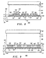
- FIG. 8 is a cross-sectional view similar to that of FIGs. 3 and 7 of a field emission device 300 in accordance with the present invention.
- Field emission device 300 includes a spacer 350, which has a plurality of spacer grooves 359.
- Spacer grooves 359 are defined by a second edge 355 of spacer 350.
- a first edge 357 of spacer 350 makes contact with anode 190.
- Spacer grooves 359 overlie cathodes 120.
- Spacer 350 includes a rib of a hard dielectric material, such as a glass. Spacer grooves 359 can be formed by sawing into one of the edges of the rib of the hard dielectric material using a diamond saw.
- Field emission device 300 includes a cathode structure 380, which is configured similar to cathode structures 180, 280 of field emission devices 100, 200, respectively, except that it does not include spacer pads. Instead, the regions of cathode structure 380 between cathodes 120 include portions of dielectric layer 124 and portions of a spacer contact layer 385. Spacer contact layer 385 is formed in the manner described with reference to spacer contact layer 185 of FIG. 5. Alternatively, a spacer contact layer, such as spacer contact layer 142 described with reference to FIGs. 1 - 4, can be employed. A conductive layer 352 is formed on second edge 355 in the manner described with reference to conductive layer 152 of FIGs. 1 - 7.
- a first portion 386 of the surface of cathode structure 380 overlies cathodes 120 along the length of spacer 350 and is defined by spacer contact layer 385; a second portion 388 of the surface of cathode structure 380 is disposed between cathodes 120 along the length of spacer 350 and is also defined by spacer contact layer 385.
- Conductive layer 352 physically contacts the surface of cathode structure 380 at second portion 388.
- Spacer grooves 359 and first portion 386 of the surface of cathode structure 380 define a plurality of gaps 387 that overlie cathodes 120.
- Gaps 387 have a height 383 h g that is sufficient to prevent contact between second edge 355 of spacer 350 and cathodes 120 during the evacuation of field emission device 300.
- the maximum height of cathode structure 380 along the length of spacer 350 is equal to a first height 382 h c of cathode structure 380 at cathodes 120.
- FIG. 9 is a cross-sectional view similar to that of FIG. 8 of a field emission device 400 in accordance with the present invention.
- a cathode structure 480 has a spacer contact layer 485 that further includes a plurality of ball bumps 410.
- Ball bumps 410 are disposed on spacer contact layer 385 between cathodes 120 and define a second portion 488 of the surface of cathode structure 480.
- Second portion 488 of the surface of cathode structure 480 is disposed between cathodes 120 along the length of spacer 150.
- Ball bumps 410 include deposits of a metal, such as gold, aluminum, and the like.
- Ball bumps 410 are bonded by thermal compression techniques to spacer contact layer 385 and to conductive layer 152 of spacer 150. Further illustrated in FIG. 9, a plurality of gaps 487 are defined by ball bumps 410, conductive layer 152, and first portion 386 of the surface of cathode structure 480. A height 483 of gaps 487 can be controlled by adjusting the size of ball bumps 410.
- Cathode structure 480 has first height 382 h c at cathodes 120 along the length of spacer 150.
- Cathode structure 480 also has a second height 481 h p at ball bumps 410. Second height 481 is greater than first height 382.
Landscapes
- Cathode-Ray Tubes And Fluorescent Screens For Display (AREA)
- Vessels, Lead-In Wires, Accessory Apparatuses For Cathode-Ray Tubes (AREA)
- Electrodes For Cathode-Ray Tubes (AREA)
Description
Claims (5)
- A field emission device (100, 200) comprising:an anode (190) having a major surface;a substrate (110) having a major surface;a cathode structure (180) having an electron emitter (170), a first cathode (120) a second cathode (120), and a surface, the first and second cathodes (120) disposed on the major surface of the substrate (110), the surface of the cathode structure (180) having a first portion (186) overlying the first and second cathodes (120) and a second portion (188) coextensive with the first portion (186) and positioned between the first and second cathodes(120) and a spacer contact layer (142) wherein the second portion (188) of the surface of the cathode structure (180) is defined by the spacer contact layer (142);the surface of the cathode structure (180) spaced apart from the major surface of the anode (190) to define an interspace region (195) therebetween;a spacer (150) disposed in the interspace region (195) and having a first non-conductive edge (157), and a second non-conductive edge (155), whereby the first non-conductive edge (157) is disposed in abutting engagement with the major surface of the anode (190), the electron emitter (170) of the cathode structure (180) spaced apart from the second non-conductive edge (155) of the spacer (150); anda conductive layer (152) disposed on the second non-conductive edge (155) of the spacer (150) wherein the conductive layer (152) is disposed in abutting engagement with the spacer contact layer (142) at the second portion (188) of the surface of the cathode structure (180), the conductive layer (152) and the first portion (186) of the surface of the cathode structure (180) defining a first gap (187) overlying the first cathode (120) and a second gap (187) overlying the second cathode (120), whereby the first and second gaps (187) prevent physical and electrical contacts between the conductive layer (152) of the spacer (150) and the first and second cathodes (120).
- The field emission device of claim 1, wherein the spacer (350) further includes first and second spacer grooves (359) defined by the second edge (355) of the spacer (350), the first spacer groove (359) overlying the first cathode (120) and the second spacer groove (359) overlying the second cathode (120).
- The field emission device of claim 1, wherein the cathode structure (480) further includes a ball bump (410) disposed between the first and second cathodes (120) and defining the second portion (488) of the surface of the cathode structure (480), and wherein the first portion (386) of the surface of the cathode structure (480) has a first height (382) from the major surface of the substrate (110) and the second portion (488) of the surface of the cathode structure (480) has a second height (481) from the major surface of the substrate (110), the second height (481) being greater than the first height (382).
- The field emission device of claim 1, wherein the cathode structure (180) further includes a spacer pad (130) disposed between the first and second cathodes (120) and defining the second portion (188) of the surface of the cathode structure (180), and wherein the first portion (186) of the surface of the cathode structure (180) has a first height (182) from the major surface of the substrate (110) and the second portion (188) of the surface of the cathode structure (180) has a second height (181) from the major surface of the substrate (110), the second height (181) being greater than the first height (182).
- The field emission device of claim 4, wherein the cathode structure (180) further includes a dielectric layer (124) disposed on the first and second cathodes (120), and wherein the spacer pad (130) includes a ballast pad layer (118) disposed on the major surface of the substrate (110), a cathode p ad layer (122) disposed on the ballast pad layer (118), and a portion of the dielectric layer (124) disposed on the cathode pad layer (122).
Applications Claiming Priority (3)
| Application Number | Priority Date | Filing Date | Title |
|---|---|---|---|
| US854861 | 1997-05-12 | ||
| US08/854,861 US5831383A (en) | 1997-05-12 | 1997-05-12 | Spacer pads for field emission device |
| PCT/US1998/002453 WO1998052204A1 (en) | 1997-05-12 | 1998-02-06 | Spacer pads for field emission device |
Publications (3)
| Publication Number | Publication Date |
|---|---|
| EP0990249A1 EP0990249A1 (en) | 2000-04-05 |
| EP0990249A4 EP0990249A4 (en) | 2000-04-26 |
| EP0990249B1 true EP0990249B1 (en) | 2004-01-21 |
Family
ID=25319713
Family Applications (1)
| Application Number | Title | Priority Date | Filing Date |
|---|---|---|---|
| EP98906243A Expired - Lifetime EP0990249B1 (en) | 1997-05-12 | 1998-02-06 | Spacer pads for field emission device |
Country Status (5)
| Country | Link |
|---|---|
| US (1) | US5831383A (en) |
| EP (1) | EP0990249B1 (en) |
| DE (1) | DE69821232T2 (en) |
| TW (1) | TW382733B (en) |
| WO (1) | WO1998052204A1 (en) |
Families Citing this family (1)
| Publication number | Priority date | Publication date | Assignee | Title |
|---|---|---|---|---|
| KR20070046537A (en) * | 2005-10-31 | 2007-05-03 | 삼성에스디아이 주식회사 | Electron emission indicator |
Family Cites Families (8)
| Publication number | Priority date | Publication date | Assignee | Title |
|---|---|---|---|---|
| US5675212A (en) * | 1992-04-10 | 1997-10-07 | Candescent Technologies Corporation | Spacer structures for use in flat panel displays and methods for forming same |
| US5614781A (en) * | 1992-04-10 | 1997-03-25 | Candescent Technologies Corporation | Structure and operation of high voltage supports |
| NL9100122A (en) * | 1991-01-25 | 1992-08-17 | Philips Nv | DISPLAY DEVICE. |
| CA2073923C (en) * | 1991-07-17 | 2000-07-11 | Hidetoshi Suzuki | Image-forming device |
| JP2653008B2 (en) * | 1993-01-25 | 1997-09-10 | 日本電気株式会社 | Cold cathode device and method of manufacturing the same |
| GB2276270A (en) * | 1993-03-18 | 1994-09-21 | Ibm | Spacers for flat panel displays |
| JP3476215B2 (en) * | 1993-07-13 | 2003-12-10 | 富士通株式会社 | Surface discharge type plasma display panel |
| JP3083076B2 (en) * | 1995-04-21 | 2000-09-04 | キヤノン株式会社 | Image forming device |
-
1997
- 1997-05-12 US US08/854,861 patent/US5831383A/en not_active Expired - Fee Related
-
1998
- 1998-02-06 DE DE69821232T patent/DE69821232T2/en not_active Expired - Fee Related
- 1998-02-06 WO PCT/US1998/002453 patent/WO1998052204A1/en not_active Ceased
- 1998-02-06 EP EP98906243A patent/EP0990249B1/en not_active Expired - Lifetime
- 1998-02-24 TW TW087102624A patent/TW382733B/en active
Also Published As
| Publication number | Publication date |
|---|---|
| EP0990249A4 (en) | 2000-04-26 |
| DE69821232T2 (en) | 2004-12-02 |
| EP0990249A1 (en) | 2000-04-05 |
| TW382733B (en) | 2000-02-21 |
| US5831383A (en) | 1998-11-03 |
| WO1998052204A1 (en) | 1998-11-19 |
| DE69821232D1 (en) | 2004-02-26 |
Similar Documents
| Publication | Publication Date | Title |
|---|---|---|
| US5708325A (en) | Display spacer structure for a field emission device | |
| US6144144A (en) | Patterned resistor suitable for electron-emitting device | |
| US6172456B1 (en) | Field emission display | |
| US5717287A (en) | Spacers for a flat panel display and method | |
| JP3070469B2 (en) | Field emission cold cathode and method of manufacturing the same | |
| EP0985220B1 (en) | Fabrication of electron-emitting device having ladder-like emitter electrode | |
| WO1995017762A1 (en) | Lateral field emitter device and method of manufacturing same | |
| US5760535A (en) | Field emission device | |
| WO1996008028A1 (en) | Field emission display device | |
| JP2002505503A5 (en) | ||
| KR20000064852A (en) | Charge-consuming field emission devices | |
| US5719406A (en) | Field emission device having a charge bleed-off barrier | |
| US6626720B1 (en) | Method of manufacturing vacuum gap dielectric field emission triode and apparatus | |
| US5691600A (en) | Edge electron emitters for an array of FEDS | |
| US5614786A (en) | Fluorescent display device with insulated grid | |
| US5831383A (en) | Spacer pads for field emission device | |
| WO1999045559A2 (en) | Field emission display having an ion shield | |
| JPH05159696A (en) | Field emission electronic device | |
| US5828288A (en) | Pedestal edge emitter and non-linear current limiters for field emitter displays and other electron source applications | |
| US6084339A (en) | Field emission device having an electroplated structure and method for the fabrication thereof | |
| JP2000348601A (en) | Electron emission source, method of manufacturing the same, and display device using the electron emission source | |
| US6060219A (en) | Methods of forming electron emitters, surface conduction electron emitters and field emission display assemblies | |
| JP2856672B2 (en) | Field electron emission device and method of manufacturing the same | |
| JPH06111735A (en) | Display device mounted with field emission type cathode and mounting method of field emission type cathode | |
| KR100459878B1 (en) | The method for manufacturing field emission display spacer |
Legal Events
| Date | Code | Title | Description |
|---|---|---|---|
| PUAI | Public reference made under article 153(3) epc to a published international application that has entered the european phase |
Free format text: ORIGINAL CODE: 0009012 |
|
| 17P | Request for examination filed |
Effective date: 19991213 |
|
| AK | Designated contracting states |
Kind code of ref document: A1 Designated state(s): DE FR GB NL |
|
| A4 | Supplementary search report drawn up and despatched |
Effective date: 20000309 |
|
| AK | Designated contracting states |
Kind code of ref document: A4 Designated state(s): DE FR GB NL |
|
| RIC1 | Information provided on ipc code assigned before grant |
Free format text: 7H 01J 1/88 A, 7H 01J 29/02 B |
|
| 17Q | First examination report despatched |
Effective date: 20020603 |
|
| GRAP | Despatch of communication of intention to grant a patent |
Free format text: ORIGINAL CODE: EPIDOSNIGR1 |
|
| GRAS | Grant fee paid |
Free format text: ORIGINAL CODE: EPIDOSNIGR3 |
|
| GRAA | (expected) grant |
Free format text: ORIGINAL CODE: 0009210 |
|
| AK | Designated contracting states |
Kind code of ref document: B1 Designated state(s): DE FR GB NL |
|
| REG | Reference to a national code |
Ref country code: GB Ref legal event code: FG4D |
|
| REF | Corresponds to: |
Ref document number: 69821232 Country of ref document: DE Date of ref document: 20040226 Kind code of ref document: P |
|
| ET | Fr: translation filed | ||
| PLBE | No opposition filed within time limit |
Free format text: ORIGINAL CODE: 0009261 |
|
| STAA | Information on the status of an ep patent application or granted ep patent |
Free format text: STATUS: NO OPPOSITION FILED WITHIN TIME LIMIT |
|
| 26N | No opposition filed |
Effective date: 20041022 |
|
| PGFP | Annual fee paid to national office [announced via postgrant information from national office to epo] |
Ref country code: NL Payment date: 20060109 Year of fee payment: 9 |
|
| PGFP | Annual fee paid to national office [announced via postgrant information from national office to epo] |
Ref country code: FR Payment date: 20060202 Year of fee payment: 9 |
|
| PGFP | Annual fee paid to national office [announced via postgrant information from national office to epo] |
Ref country code: DE Payment date: 20060228 Year of fee payment: 9 |
|
| GBPC | Gb: european patent ceased through non-payment of renewal fee |
Effective date: 20070206 |
|
| NLV4 | Nl: lapsed or anulled due to non-payment of the annual fee |
Effective date: 20070901 |
|
| REG | Reference to a national code |
Ref country code: FR Ref legal event code: ST Effective date: 20071030 |
|
| PG25 | Lapsed in a contracting state [announced via postgrant information from national office to epo] |
Ref country code: NL Free format text: LAPSE BECAUSE OF NON-PAYMENT OF DUE FEES Effective date: 20070901 Ref country code: DE Free format text: LAPSE BECAUSE OF NON-PAYMENT OF DUE FEES Effective date: 20070901 |
|
| PG25 | Lapsed in a contracting state [announced via postgrant information from national office to epo] |
Ref country code: GB Free format text: LAPSE BECAUSE OF NON-PAYMENT OF DUE FEES Effective date: 20070206 Ref country code: FR Free format text: LAPSE BECAUSE OF NON-PAYMENT OF DUE FEES Effective date: 20070228 |
|
| PGFP | Annual fee paid to national office [announced via postgrant information from national office to epo] |
Ref country code: GB Payment date: 20060109 Year of fee payment: 9 |