EP0989668A1 - Quadrature output oscillator device - Google Patents
Quadrature output oscillator device Download PDFInfo
- Publication number
- EP0989668A1 EP0989668A1 EP99203043A EP99203043A EP0989668A1 EP 0989668 A1 EP0989668 A1 EP 0989668A1 EP 99203043 A EP99203043 A EP 99203043A EP 99203043 A EP99203043 A EP 99203043A EP 0989668 A1 EP0989668 A1 EP 0989668A1
- Authority
- EP
- European Patent Office
- Prior art keywords
- output
- oscillator
- quadrature
- voltage controlled
- phase
- Prior art date
- Legal status (The legal status is an assumption and is not a legal conclusion. Google has not performed a legal analysis and makes no representation as to the accuracy of the status listed.)
- Granted
Links
- 238000000034 method Methods 0.000 claims description 7
- 238000010586 diagram Methods 0.000 description 5
- 230000004075 alteration Effects 0.000 description 1
- 230000035559 beat frequency Effects 0.000 description 1
- 230000005540 biological transmission Effects 0.000 description 1
- 230000007274 generation of a signal involved in cell-cell signaling Effects 0.000 description 1
- 230000010355 oscillation Effects 0.000 description 1
- 238000006467 substitution reaction Methods 0.000 description 1
Images

Classifications
-
- H—ELECTRICITY
- H03—ELECTRONIC CIRCUITRY
- H03B—GENERATION OF OSCILLATIONS, DIRECTLY OR BY FREQUENCY-CHANGING, BY CIRCUITS EMPLOYING ACTIVE ELEMENTS WHICH OPERATE IN A NON-SWITCHING MANNER; GENERATION OF NOISE BY SUCH CIRCUITS
- H03B1/00—Details
-
- H—ELECTRICITY
- H03—ELECTRONIC CIRCUITRY
- H03K—PULSE TECHNIQUE
- H03K3/00—Circuits for generating electric pulses; Monostable, bistable or multistable circuits
- H03K3/02—Generators characterised by the type of circuit or by the means used for producing pulses
- H03K3/353—Generators characterised by the type of circuit or by the means used for producing pulses by the use, as active elements, of field-effect transistors with internal or external positive feedback
- H03K3/354—Astable circuits
-
- H—ELECTRICITY
- H03—ELECTRONIC CIRCUITRY
- H03B—GENERATION OF OSCILLATIONS, DIRECTLY OR BY FREQUENCY-CHANGING, BY CIRCUITS EMPLOYING ACTIVE ELEMENTS WHICH OPERATE IN A NON-SWITCHING MANNER; GENERATION OF NOISE BY SUCH CIRCUITS
- H03B27/00—Generation of oscillations providing a plurality of outputs of the same frequency but differing in phase, other than merely two anti-phase outputs
-
- H—ELECTRICITY
- H03—ELECTRONIC CIRCUITRY
- H03B—GENERATION OF OSCILLATIONS, DIRECTLY OR BY FREQUENCY-CHANGING, BY CIRCUITS EMPLOYING ACTIVE ELEMENTS WHICH OPERATE IN A NON-SWITCHING MANNER; GENERATION OF NOISE BY SUCH CIRCUITS
- H03B5/00—Generation of oscillations using amplifier with regenerative feedback from output to input
- H03B5/08—Generation of oscillations using amplifier with regenerative feedback from output to input with frequency-determining element comprising lumped inductance and capacitance
- H03B5/12—Generation of oscillations using amplifier with regenerative feedback from output to input with frequency-determining element comprising lumped inductance and capacitance active element in amplifier being semiconductor device
- H03B5/1206—Generation of oscillations using amplifier with regenerative feedback from output to input with frequency-determining element comprising lumped inductance and capacitance active element in amplifier being semiconductor device using multiple transistors for amplification
- H03B5/1212—Generation of oscillations using amplifier with regenerative feedback from output to input with frequency-determining element comprising lumped inductance and capacitance active element in amplifier being semiconductor device using multiple transistors for amplification the amplifier comprising a pair of transistors, wherein an output terminal of each being connected to an input terminal of the other, e.g. a cross coupled pair
- H03B5/1215—Generation of oscillations using amplifier with regenerative feedback from output to input with frequency-determining element comprising lumped inductance and capacitance active element in amplifier being semiconductor device using multiple transistors for amplification the amplifier comprising a pair of transistors, wherein an output terminal of each being connected to an input terminal of the other, e.g. a cross coupled pair the current source or degeneration circuit being in common to both transistors of the pair, e.g. a cross-coupled long-tailed pair
-
- H—ELECTRICITY
- H03—ELECTRONIC CIRCUITRY
- H03B—GENERATION OF OSCILLATIONS, DIRECTLY OR BY FREQUENCY-CHANGING, BY CIRCUITS EMPLOYING ACTIVE ELEMENTS WHICH OPERATE IN A NON-SWITCHING MANNER; GENERATION OF NOISE BY SUCH CIRCUITS
- H03B5/00—Generation of oscillations using amplifier with regenerative feedback from output to input
- H03B5/08—Generation of oscillations using amplifier with regenerative feedback from output to input with frequency-determining element comprising lumped inductance and capacitance
- H03B5/12—Generation of oscillations using amplifier with regenerative feedback from output to input with frequency-determining element comprising lumped inductance and capacitance active element in amplifier being semiconductor device
- H03B5/1206—Generation of oscillations using amplifier with regenerative feedback from output to input with frequency-determining element comprising lumped inductance and capacitance active element in amplifier being semiconductor device using multiple transistors for amplification
- H03B5/1221—Generation of oscillations using amplifier with regenerative feedback from output to input with frequency-determining element comprising lumped inductance and capacitance active element in amplifier being semiconductor device using multiple transistors for amplification the amplifier comprising multiple amplification stages connected in cascade
-
- H—ELECTRICITY
- H03—ELECTRONIC CIRCUITRY
- H03B—GENERATION OF OSCILLATIONS, DIRECTLY OR BY FREQUENCY-CHANGING, BY CIRCUITS EMPLOYING ACTIVE ELEMENTS WHICH OPERATE IN A NON-SWITCHING MANNER; GENERATION OF NOISE BY SUCH CIRCUITS
- H03B5/00—Generation of oscillations using amplifier with regenerative feedback from output to input
- H03B5/08—Generation of oscillations using amplifier with regenerative feedback from output to input with frequency-determining element comprising lumped inductance and capacitance
- H03B5/12—Generation of oscillations using amplifier with regenerative feedback from output to input with frequency-determining element comprising lumped inductance and capacitance active element in amplifier being semiconductor device
- H03B5/1228—Generation of oscillations using amplifier with regenerative feedback from output to input with frequency-determining element comprising lumped inductance and capacitance active element in amplifier being semiconductor device the amplifier comprising one or more field effect transistors
-
- H—ELECTRICITY
- H03—ELECTRONIC CIRCUITRY
- H03B—GENERATION OF OSCILLATIONS, DIRECTLY OR BY FREQUENCY-CHANGING, BY CIRCUITS EMPLOYING ACTIVE ELEMENTS WHICH OPERATE IN A NON-SWITCHING MANNER; GENERATION OF NOISE BY SUCH CIRCUITS
- H03B5/00—Generation of oscillations using amplifier with regenerative feedback from output to input
- H03B5/08—Generation of oscillations using amplifier with regenerative feedback from output to input with frequency-determining element comprising lumped inductance and capacitance
- H03B5/12—Generation of oscillations using amplifier with regenerative feedback from output to input with frequency-determining element comprising lumped inductance and capacitance active element in amplifier being semiconductor device
- H03B5/1237—Generation of oscillations using amplifier with regenerative feedback from output to input with frequency-determining element comprising lumped inductance and capacitance active element in amplifier being semiconductor device comprising means for varying the frequency of the generator
- H03B5/124—Generation of oscillations using amplifier with regenerative feedback from output to input with frequency-determining element comprising lumped inductance and capacitance active element in amplifier being semiconductor device comprising means for varying the frequency of the generator the means comprising a voltage dependent capacitance
- H03B5/1243—Generation of oscillations using amplifier with regenerative feedback from output to input with frequency-determining element comprising lumped inductance and capacitance active element in amplifier being semiconductor device comprising means for varying the frequency of the generator the means comprising a voltage dependent capacitance the means comprising voltage variable capacitance diodes
-
- H—ELECTRICITY
- H03—ELECTRONIC CIRCUITRY
- H03K—PULSE TECHNIQUE
- H03K3/00—Circuits for generating electric pulses; Monostable, bistable or multistable circuits
- H03K3/02—Generators characterised by the type of circuit or by the means used for producing pulses
- H03K3/027—Generators characterised by the type of circuit or by the means used for producing pulses by the use of logic circuits, with internal or external positive feedback
- H03K3/03—Astable circuits
- H03K3/0315—Ring oscillators
- H03K3/0322—Ring oscillators with differential cells
Definitions
- the present invention relates in general to receiving techniques and more particularly to a quadrature output oscillator device.
- quadrature outputs generated from voltage controlled oscillators are not ideal, i.e. the phase difference between the in-phase and quadrature-phase signal components are 90° ⁇ some error.
- the error in this phase difference is mostly due to device mismatch.
- many receiver topologies rely on precise quadrature in order to achieve frequency image rejection in the received signal.
- the quality of reception is degraded, in the presence of frequency images in the received signal, due to the imprecise quadrature component signal generation in the receiver.
- Frequency image rejection could be performed by passive filters, but these passive filters result in increased design complexities and higher costs. Therefore, it is desirable to have precise quadrature to achieve the desired receiver circuit performance.
- the present application discloses a quadrature output oscillator device that substantially eliminates or reduces disadvantages and problems associated with conventional quadrature output voltage controlled oscillator devices.
- a quadrature output oscillator device that includes a first voltage controlled oscillator that generates a first output and a second output, wherein the second output of the first voltage controlled oscillator is an in-phase signal component.
- a second voltage controlled oscillator also generates a first output and a second output, wherein the second output of the second voltage controlled oscillator is a quadrature-phase signal component.
- a first amplifier receives the first and second outputs from the second voltage controlled oscillator. The first amplifier generates a first feedback signal coupled to the first output of the first voltage controlled oscillator and a second feedback signal coupled to the second output of the first voltage controlled oscillator.
- a second amplifier receives the first and second outputs from the first voltage controlled oscillator.
- the second amplifier generates a first feedback signal coupled to the first output of the second voltage controlled oscillator and a second feedback signal coupled to the second output of the second voltage controlled oscillator.
- a gain adjustment unit controls a gain of the first amplifier and the second amplifier in order to provide ideal in-phase and quadrature-phase signal components at the second output of the first voltage controlled oscillator and the second output of the second voltage controlled oscillator, respectively.
- the disclosed quadrature output oscillator device provides various technical advantages over conventional quadrature output voltage controlled oscillator devices. For example, one technical advantage is to provide ideal quadrature outputs from voltage controlled oscillators. Another technical advantage is to eliminate the use of passive filters in receiver topologies. Yet another technical advantage is in compensating for device mismatches within voltage controlled oscillators. Other technical advantages may be readily ascertainable by those skilled in the art from the following figures, description, and claims.
- FIGURE 1 is a simplified schematic diagram of a radio frequency signal receiver 10.
- Receiver 10 includes an antenna 12 for receiving a radio frequency signal over a transmission frequency.
- the radio frequency signal is processed by a filter 14 and enhanced by an amplifier 16.
- the radio frequency signal after being filtered and amplified, is applied to a first mixer 18 and a second mixer 20 of a first mixing stage 21.
- the first mixer 18 is controlled by an in-phase signal component I a generated by a quadrature output oscillator device 22.
- the second mixer 20 is controlled by a quadrature-phase signal component Q a generated by quadrature output oscillator device 22.
- First mixer 18 generates an output that is provided to a third mixer 24 and a fourth mixer 26 of a second mixing stage 27.
- Third mixer 24 is controlled by an in-phase signal component I b and fourth mixer 26 is controlled by a quadrature-phase signal component Q b generated by another quadrature output oscillator device 29.
- Second mixer 20 generates an output that is provided to a fifth mixer 28 and a sixth mixer 30.
- Fifth mixer 28 is controlled by in-phase signal component I b and sixth mixer is controlled by quadrature-phase signal component Q b .
- Outputs from third mixer 24 and sixth mixer 30 are provided to a selector 32 in order to generate an in-phase representation of the radio frequency signal.
- Outputs from fourth mixer 26 and fifth mixer 28 are provided to a selector 34 in order to generate a quadrature-phase representation of the radio frequency signal.
- the desired down-converted signal can be obtained if selector 32 adds the inputs it receives and selector 34 subtracts the inputs it receives, or vice versa wherein selector 32 acts as a subtractor and selector 34 acts as an adder.
- Quadrature output oscillator device 29 is preferably different in implementation from quadrature output oscillator device 22 in that the required oscillator operates at a much lower frequency, and hence does not include inductor devices on-chip.
- the difference in device type is mainly due to the fact that inductors are difficult to implement on an integrated circuit in order to provide the required lower frequency output.
- the frequency of the radio frequency signal received at antenna 12 could be around 1.9 GHz.
- the frequency generated by quadrature output device 22 is in the range of 1.5-1.7 GHz.
- Quadrature output device 29 generates the difference between the frequency of the radio frequency signal received at antenna 12 and the frequency generated by quadrature output device 22, that is 200-400 MHz.
- the mixers within receiver 10 are used to down-convert the frequency of the radio-frequency signal received at antenna 12 to an intermediate frequency that is the beat frequency of the radio-frequency signal and the local oscillator frequency of the quadrature output oscillator device 22.
- the image signal will be down converted to the same intermediate frequency as that produced by the mixing of the oscillator frequency and the received radio signal.
- the down-converted image signal will interfere with proper reception of the desired down-converted radio signal and degrade receiver performance. Extra image-rejection filters could be used before the mixers to reject this image signal.
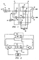
- FIGURE 2 shows a simplified block diagram of quadrature output oscillator device 22 that produces ideal quadrature outputs.
- Quadrature output oscillator device 22 includes a first voltage controlled oscillator 40 that generates outputs A and B. Outputs A and B are fed back as inputs to first voltage controlled oscillator 40.
- Quadrature output oscillator device 22 includes a second voltage controlled oscillator 44 that generates outputs C and D. Outputs C and D are fed back as inputs to second voltage controlled oscillator 44.
- First amplifier 42 generates outputs to drive the feedback A and B signal lines of first voltage controlled oscillator 40 in response to Outputs D and C, respectively, from second voltage controlled oscillator 44.
- Second amplifier 46 generates outputs to drive the feedback C and D signal lines of second voltage controlled oscillator 44 in response to Outputs A and B, respectively, from first voltage controlled oscillator 40.
- a gain adjust unit 48 controls a gain for both first amplifier 42 and second amplifier 46 in order to provide ideal quadrature components I and Q from first voltage controlled oscillator 40 and second voltage controlled oscillator 44, respectively.
- FIGURE 3 is a schematic diagram of quadrature output oscillator device 22.
- First voltage controlled oscillator 40 and second voltage controlled oscillator 44 each include a cross-coupled pair of transistors, respectively M A -M B and M C -M D .
- Inductor loads are provided by inductors L 1 , L 2 , L 3 , and L 4 .
- the center frequency is set and frequency tuning is accomplished by the use of varactor diodes D 1 , D 2 , D 3 , and D 4 which are preferably implemented using p + -n junctions in n-wells.
- the feedback arrangement provided through first amplifier 42 and second amplifier 46 assist in locking first voltage controlled oscillator 40 with second voltage controlled oscillator 44 such that they become stable when they are quadrature locked.
- Transistors M BIAS1 , M BIAS2 , M BIAS3 , and M BIAS4 provide the current sources for first voltage controlled oscillator 40, second voltage controlled oscillator 44, first amplifier 42, and second amplifier 46, respectively. These current sources are preferably maintained at a fixed level in order to prevent large swings in the circuit due to unbounded growth of oscillations, resulting in large spikes on the V DD supply line that may cause damage to n-well devices tied thereto.
- gain adjust unit 48 is provided. For example, a 1% mismatch in device characteristics may cause a 4 to 5 error in quadrature.
- the bias through M 1 -M 2 transistor pair of first amplifier 42 and M 3 -M 4 transistor pair of second amplifier 46 is varied by changing V CNTL+ and V CNTL- inputs into gain adjust unit 48. Controlling the bias through M 1 -M 2 and M 3 -M 4 effectively changes the relative strength of the feedback from M A -M B to M C -M D and vice versa.
- gain adjust unit 48 can be used to electrically trim the phase of the in-phase I and quadrature-phase Q signal components such that they are exactly 90 apart.
Landscapes
- Inductance-Capacitance Distribution Constants And Capacitance-Resistance Oscillators (AREA)
- Stabilization Of Oscillater, Synchronisation, Frequency Synthesizers (AREA)
- Control Of Amplification And Gain Control (AREA)
- Digital Transmission Methods That Use Modulated Carrier Waves (AREA)
- Oscillators With Electromechanical Resonators (AREA)
Abstract
Description
- The present invention relates in general to receiving techniques and more particularly to a quadrature output oscillator device.
- Typically, quadrature outputs generated from voltage controlled oscillators are not ideal, i.e. the phase difference between the in-phase and quadrature-phase signal components are 90° ± some error. The error in this phase difference is mostly due to device mismatch. However, many receiver topologies rely on precise quadrature in order to achieve frequency image rejection in the received signal. The quality of reception is degraded, in the presence of frequency images in the received signal, due to the imprecise quadrature component signal generation in the receiver. Frequency image rejection could be performed by passive filters, but these passive filters result in increased design complexities and higher costs. Therefore, it is desirable to have precise quadrature to achieve the desired receiver circuit performance.
- From the foregoing, it may be appreciated that a need has arisen for a receiver that implements ideal in-phase and quadrature-phase signal components in order to effectively achieve proper frequency image rejection. The present application discloses a quadrature output oscillator device that substantially eliminates or reduces disadvantages and problems associated with conventional quadrature output voltage controlled oscillator devices.
- According to a disclosed embodiment there is provided a quadrature output oscillator device that includes a first voltage controlled oscillator that generates a first output and a second output, wherein the second output of the first voltage controlled oscillator is an in-phase signal component. A second voltage controlled oscillator also generates a first output and a second output, wherein the second output of the second voltage controlled oscillator is a quadrature-phase signal component. A first amplifier receives the first and second outputs from the second voltage controlled oscillator. The first amplifier generates a first feedback signal coupled to the first output of the first voltage controlled oscillator and a second feedback signal coupled to the second output of the first voltage controlled oscillator. A second amplifier receives the first and second outputs from the first voltage controlled oscillator. The second amplifier generates a first feedback signal coupled to the first output of the second voltage controlled oscillator and a second feedback signal coupled to the second output of the second voltage controlled oscillator. A gain adjustment unit controls a gain of the first amplifier and the second amplifier in order to provide ideal in-phase and quadrature-phase signal components at the second output of the first voltage controlled oscillator and the second output of the second voltage controlled oscillator, respectively.
- The disclosed quadrature output oscillator device provides various technical advantages over conventional quadrature output voltage controlled oscillator devices. For example, one technical advantage is to provide ideal quadrature outputs from voltage controlled oscillators. Another technical advantage is to eliminate the use of passive filters in receiver topologies. Yet another technical advantage is in compensating for device mismatches within voltage controlled oscillators. Other technical advantages may be readily ascertainable by those skilled in the art from the following figures, description, and claims.
- For a more complete understanding of the present invention and the advantages thereof, reference is now made to the following description taken in conjunction with the accompanying drawings, wherein like reference numerals represent like parts, in which:
- FIGURE 1 is a simplified schematic representation of an image reject receiver;
- FIGURE 2 is a simplified block diagram of a quadrature output oscillator device within the receiver; and
- FIGURE 3 is a schematic diagram of the quadrature output oscillator device.
-
- FIGURE 1 is a simplified schematic diagram of a radio
frequency signal receiver 10.Receiver 10 includes anantenna 12 for receiving a radio frequency signal over a transmission frequency. The radio frequency signal is processed by afilter 14 and enhanced by anamplifier 16. The radio frequency signal, after being filtered and amplified, is applied to afirst mixer 18 and asecond mixer 20 of afirst mixing stage 21. Thefirst mixer 18 is controlled by an in-phase signal component Ia generated by a quadratureoutput oscillator device 22. Thesecond mixer 20 is controlled by a quadrature-phase signal component Qa generated by quadratureoutput oscillator device 22.First mixer 18 generates an output that is provided to athird mixer 24 and afourth mixer 26 of asecond mixing stage 27.Third mixer 24 is controlled by an in-phase signal component Ib andfourth mixer 26 is controlled by a quadrature-phase signal component Qb generated by another quadratureoutput oscillator device 29.Second mixer 20 generates an output that is provided to afifth mixer 28 and asixth mixer 30.Fifth mixer 28 is controlled by in-phase signal component Ib and sixth mixer is controlled by quadrature-phase signal component Qb. Outputs fromthird mixer 24 andsixth mixer 30 are provided to aselector 32 in order to generate an in-phase representation of the radio frequency signal. Outputs fromfourth mixer 26 andfifth mixer 28 are provided to aselector 34 in order to generate a quadrature-phase representation of the radio frequency signal. Depending on the phases of the oscillators applied to the various mixers, the desired down-converted signal can be obtained ifselector 32 adds the inputs it receives andselector 34 subtracts the inputs it receives, or vice versa whereinselector 32 acts as a subtractor andselector 34 acts as an adder. - Quadrature
output oscillator device 29 is preferably different in implementation from quadratureoutput oscillator device 22 in that the required oscillator operates at a much lower frequency, and hence does not include inductor devices on-chip. The difference in device type is mainly due to the fact that inductors are difficult to implement on an integrated circuit in order to provide the required lower frequency output. As an example, the frequency of the radio frequency signal received atantenna 12 could be around 1.9 GHz. The frequency generated byquadrature output device 22 is in the range of 1.5-1.7 GHz.Quadrature output device 29 generates the difference between the frequency of the radio frequency signal received atantenna 12 and the frequency generated byquadrature output device 22, that is 200-400 MHz. - The mixers within
receiver 10 are used to down-convert the frequency of the radio-frequency signal received atantenna 12 to an intermediate frequency that is the beat frequency of the radio-frequency signal and the local oscillator frequency of the quadratureoutput oscillator device 22. Any signal located at a frequency lower than the oscillator frequency, at a spacing equal to that between the oscillator frequency and the received radio signal frequency, is defined to be an image signal. The image signal will be down converted to the same intermediate frequency as that produced by the mixing of the oscillator frequency and the received radio signal. The down-converted image signal will interfere with proper reception of the desired down-converted radio signal and degrade receiver performance. Extra image-rejection filters could be used before the mixers to reject this image signal. However these filters are difficult to integrate on to the same circuit asreceiver 10. The mixers withinreceiver 10 are used here to eliminate this down-converted frequency. These mixers rely upon the quadrature property of the quadratureoutput oscillator device 22. However, the down-converted frequency may not be totally eliminated if there is not a true quadrature relationship between in-phase component and the quadrature phase component Q generated by quadratureoutput oscillator device 22. - FIGURE 2 shows a simplified block diagram of quadrature
output oscillator device 22 that produces ideal quadrature outputs. Quadratureoutput oscillator device 22 includes a first voltage controlledoscillator 40 that generates outputs A and B. Outputs A and B are fed back as inputs to first voltage controlledoscillator 40. Quadratureoutput oscillator device 22 includes a second voltage controlledoscillator 44 that generates outputs C and D. Outputs C and D are fed back as inputs to second voltage controlledoscillator 44.First amplifier 42 generates outputs to drive the feedback A and B signal lines of first voltage controlledoscillator 40 in response to Outputs D and C, respectively, from second voltage controlledoscillator 44.Second amplifier 46 generates outputs to drive the feedback C and D signal lines of second voltage controlledoscillator 44 in response to Outputs A and B, respectively, from first voltage controlledoscillator 40. A gain adjustunit 48 controls a gain for bothfirst amplifier 42 andsecond amplifier 46 in order to provide ideal quadrature components I and Q from first voltage controlledoscillator 40 and second voltage controlledoscillator 44, respectively. - FIGURE 3 is a schematic diagram of quadrature
output oscillator device 22. First voltage controlledoscillator 40 and second voltage controlledoscillator 44 each include a cross-coupled pair of transistors, respectively MA-MB and MC-MD. Inductor loads are provided by inductors L1, L2, L3, and L4. The center frequency is set and frequency tuning is accomplished by the use of varactor diodes D1, D2, D3, and D4 which are preferably implemented using p+-n junctions in n-wells. The feedback arrangement provided throughfirst amplifier 42 andsecond amplifier 46 assist in locking first voltage controlledoscillator 40 with second voltage controlledoscillator 44 such that they become stable when they are quadrature locked. - Transistors MBIAS1, MBIAS2, MBIAS3, and MBIAS4 provide the current sources for first voltage controlled
oscillator 40, second voltage controlledoscillator 44,first amplifier 42, andsecond amplifier 46, respectively. These current sources are preferably maintained at a fixed level in order to prevent large swings in the circuit due to unbounded growth of oscillations, resulting in large spikes on the VDD supply line that may cause damage to n-well devices tied thereto. - In order to compensate for device mismatches within quadrature
output oscillator device 22 that may yield deviations from ideal quadrature outputs, gain adjustunit 48 is provided. For example, a 1% mismatch in device characteristics may cause a 4 to 5 error in quadrature. The bias through M1-M2 transistor pair offirst amplifier 42 and M3-M4 transistor pair ofsecond amplifier 46 is varied by changing VCNTL+ and VCNTL- inputs into gain adjustunit 48. Controlling the bias through M1-M2 and M3-M4 effectively changes the relative strength of the feedback from MA-MB to MC-MD and vice versa. By changing the relative strength of feedback, adjustments to the phase of the I and Q outputs can be accomplished in order to produce ideal quadrature components. Thus, gain adjustunit 48 can be used to electrically trim the phase of the in-phase I and quadrature-phase Q signal components such that they are exactly 90 apart. - Thus, it is apparent that there has been provided, in accordance with the teachings of the present application, a quadrature output device that satisfies the advantages set forth above. Although the present invention has been described in detail, it should be understood that various changes, substitutions, and alterations may be readily ascertainable by those skilled in the art and which may be made herein without departing from the spirit and scope of the present invention.
Claims (15)
- A quadrature output oscillator device, comprising:a first voltage controlled oscillator for generating a first output and a second output, the second output of the first voltage controlled oscillator comprising an in-phase signal component;a second voltage controlled oscillator for generating a first output and a second output, the second output of the second voltage controlled oscillator comprising a quadrature-phase signal component;a first amplifier for receiving the first and second outputs from the second voltage controlled oscillator, and for generating a first feedback signal coupled to the first output of the first voltage controlled oscillator and a second feedback signal coupled to the second output of the first voltage controlled oscillator;a second amplifier for receiving the first and second outputs from the first voltage controlled oscillator, and for generating a first feedback signal coupled to the first output of the second voltage controlled oscillator and a second feedback signal coupled to the second output of the second voltage controlled oscillator; anda gain adjust unit for controling a gain of the first amplifier and the second amplifier to provide ideal in-phase and quadrature-phase signal components at the second output of the first voltage controlled oscillator and the second output of the second voltage controlled oscillator, respectively.
- The quadrature output oscillator device of Claim 1, wherein the gain adjust unit is arranged for receiving a control signal for controling the gain of each of the first and second amplifiers.
- The quadrature output oscillator device of any preceding claim, wherein the first and second voltage controlled oscillators include varactor diodes for setting and tuning the in-phase signal component and the quadrature-phase signal component generated by the first and second voltage controlled oscillators, respectively.
- The quadrature output oscillator device of any preceding claim, wherein the first and second amplifiers are arranged for locking the first and second voltage controlled oscillators such that they provide stable outputs when they are quadrature locked.
- The quadrature output oscillator device of any preceding claim, wherein the first and second voltage controlled oscillators and the first and second amplifiers each include a bias transistor for maintaining current at a fixed level to prevent voltage spikes from occurring on a supply line of the first and second voltage controlled oscillators.
- The quadrature output oscillator device of any preceding claim, wherein the first and second voltage controlled oscillators each include a cross-coupled pair of transistors, said cross-coupled pairs of transistors coupled to inductor loads that resonate with varactor diodes to provide their respective second outputs.
- The quadrature output oscillator device of any preceding claim, wherein the control signal is arranged for controlling a strength of feedback from the first voltage controlled oscillator to the second voltage controlled oscillator and vice versa.
- The quadrature output oscillator device of any preceding claims, wherein the gain adjust unit is arranged for controlling gain of the first and second amplifiers in response to a differential control signal.
- The quadrature output oscillator device of any preceding claims, wherein a phase of the in-phase signal component and the quadrature-phase signal component is arranged to be corrected in response to control of the gain by the gain adjust unit.
- A method of providing ideal in-phase and quadrature phase signal components, comprising:generating a first output and a second output from a first oscillator, the second output of the first oscillator comprising an in-phase signal component;generating a first output and a second output from a second oscillator, the second output of the second oscillator comprising a quadrature-phase signal component;generating a first feedback signal in response to the first and second outputs of the second oscillator, the first feedback signal arranged for driving the first output of the first oscillator;generating a second feedback signal in response to the first and second outputs of the second oscillator, the second feedback signal arranged for driving the second output of the first oscillator;generating a third feedback signal in response to the first and second outputs of the first oscillator, the third feedback signal arranged for driving the first output of the second oscillator;generating a fourth feedback signal in response to the first and second outputs of the first oscillator, the fourth feedback signal arranged for driving the second output of the second oscillator; andcontrolling a strength of the first, second, third, and fourth feedback signals such that the in-phase and quadrature phase signal components are substantially ninety degrees out of phase with respect to each other.
- The method of Claim 10, further comprising:setting a center frequency for the first and second oscillators.
- The method of Claim 10 or Claim 11, further comprising:tuning a frequency of the first and second oscillators to a desired level.
- The method of any of Claims 10 to 12 further comprising:receiving one or more control signals for adjusting the strength of the first, second, third, 'and fourth feedback signals.
- The method of any of Claims 10-13, further comprising:controlling a current level in the first and second oscillators for preventing voltage spikes from occurring therein.
- The method of any of Claims 10-14, further comprising:locking the first, second, third, and fourth feedback signals upon reaching an ideal quadrature relationship between the in-phase signal component and the quadrature-phase signal component.
Applications Claiming Priority (2)
| Application Number | Priority Date | Filing Date | Title |
|---|---|---|---|
| US10140498P | 1998-09-22 | 1998-09-22 | |
| US101404P | 1998-09-22 |
Publications (2)
| Publication Number | Publication Date |
|---|---|
| EP0989668A1 true EP0989668A1 (en) | 2000-03-29 |
| EP0989668B1 EP0989668B1 (en) | 2003-05-14 |
Family
ID=22284476
Family Applications (1)
| Application Number | Title | Priority Date | Filing Date |
|---|---|---|---|
| EP99203043A Expired - Lifetime EP0989668B1 (en) | 1998-09-22 | 1999-09-17 | Quadrature output oscillator device |
Country Status (7)
| Country | Link |
|---|---|
| US (1) | US6462626B1 (en) |
| EP (1) | EP0989668B1 (en) |
| JP (1) | JP2000138530A (en) |
| KR (1) | KR100763658B1 (en) |
| AT (1) | ATE240606T1 (en) |
| DE (1) | DE69907837T2 (en) |
| TW (1) | TW448628B (en) |
Cited By (1)
| Publication number | Priority date | Publication date | Assignee | Title |
|---|---|---|---|---|
| WO2003005560A1 (en) | 2001-07-05 | 2003-01-16 | Telefonaktiebolaget L M Ericsson (Publ) | Oscillator |
Families Citing this family (18)
| Publication number | Priority date | Publication date | Assignee | Title |
|---|---|---|---|---|
| JP4669130B2 (en) * | 2001-01-10 | 2011-04-13 | 川崎マイクロエレクトロニクス株式会社 | Oscillator |
| KR100498490B1 (en) * | 2003-02-28 | 2005-07-01 | 삼성전자주식회사 | Quadrature Voltage Controlled Oscillator capable of varying phase difference between in-phase output signal and quadrature output signal |
| US6937107B2 (en) * | 2003-06-30 | 2005-08-30 | Intel Corporation | Device and method of quadrature oscillation |
| US7146140B2 (en) * | 2003-06-30 | 2006-12-05 | Intel Corporation | Quadrature oscillator and methods thereof |
| DE102004008844B4 (en) * | 2004-02-20 | 2013-08-14 | Wipro Limited | RF quadrature divider |
| TWI452836B (en) * | 2004-04-01 | 2014-09-11 | St Ericsson Sa | Quadrature vco system and method |
| US20050253659A1 (en) * | 2004-05-14 | 2005-11-17 | Pierre Favrat | Current-controlled quadrature oscillator using differential gm/C cells incorporating amplitude limiters |
| US7075377B2 (en) * | 2004-06-10 | 2006-07-11 | Theta Microeletronics, Inc. | Quadrature voltage controlled oscillators with phase shift detector |
| KR100551481B1 (en) * | 2004-06-16 | 2006-02-13 | 삼성전자주식회사 | Quadrature Output Voltage Controlled Oscillator with Phase Control, Wireless Signal Transceiver with It, and Quadrature Control Method |
| US7738572B2 (en) | 2004-10-11 | 2010-06-15 | Realtek Semiconductor Corp. | Orthogonal frequency division multiplexing (OFDM) receiver capable of correcting in-phase and quadrature-phase mismatch and method thereof |
| JP2006270849A (en) * | 2005-03-25 | 2006-10-05 | Tektronix Japan Ltd | Frequency conversion circuit |
| KR100691371B1 (en) * | 2005-10-18 | 2007-03-12 | 삼성전기주식회사 | Low Power Voltage Controlled Oscillators |
| KR100721961B1 (en) * | 2005-10-28 | 2007-05-28 | 한국과학기술원 | Differential Output Oscillator Using Reactive Tunneling Diode |
| US7342462B1 (en) * | 2006-08-03 | 2008-03-11 | Agere Systems, Inc. | Quadrature LC voltage controlled oscillator with opposed bias and coupling control stages |
| KR100778338B1 (en) * | 2006-09-29 | 2007-11-22 | 한국전자통신연구원 | 4-Phase Voltage-Controlled Oscillator with Startup Circuit |
| KR20110019063A (en) * | 2009-08-19 | 2011-02-25 | 삼성전자주식회사 | Single Side Band Mixer, and Local Oscillator with the Same |
| CN101820250B (en) * | 2010-04-15 | 2012-05-30 | 复旦大学 | A Broadband Quadrature Dual-mode Voltage Controlled Oscillator |
| TWI536730B (en) * | 2014-09-24 | 2016-06-01 | 國立交通大學 | Four-phase relaxation oscillator |
Citations (2)
| Publication number | Priority date | Publication date | Assignee | Title |
|---|---|---|---|---|
| EP0523854A2 (en) * | 1991-07-18 | 1993-01-20 | STMicroelectronics Limited | Voltage controlled oscillator |
| US5561398A (en) * | 1995-05-16 | 1996-10-01 | National Semiconductor Corporation | LC-tuned voltage controlled ring oscillator |
Family Cites Families (8)
| Publication number | Priority date | Publication date | Assignee | Title |
|---|---|---|---|---|
| GB9209982D0 (en) | 1992-05-08 | 1992-06-24 | British Tech Group | Method and apparatus for amplifying modulating and demodulating |
| JP2762849B2 (en) * | 1992-07-08 | 1998-06-04 | 住友金属工業株式会社 | How to process ferro scrap |
| US5489878A (en) * | 1994-11-23 | 1996-02-06 | Analog Devices | Current-controlled quadrature oscillator based on differential gm /C cells |
| US5917383A (en) * | 1997-11-26 | 1999-06-29 | Sirf Technology, Inc. | Compact voltage controlled ring oscillator with quadrature outputs |
| US6025765A (en) * | 1998-04-08 | 2000-02-15 | Nortel Networks Corporation | Gyrator with loop amplifiers connected to inductive elements |
| US6313688B1 (en) * | 1998-07-24 | 2001-11-06 | Gct Semiconductor, Inc. | Mixer structure and method of using same |
| FR2781948B1 (en) * | 1998-07-28 | 2001-02-09 | St Microelectronics Sa | RADIO FREQUENCY RECEPTION WITH FREQUENCY CONVERSION AT LOW FREQUENCY INTERMEDIATE |
| AU2147900A (en) * | 1998-11-12 | 2000-05-29 | Broadcom Corporation | Fully integrated tuner architecture |
-
1999
- 1999-08-21 TW TW088114327A patent/TW448628B/en not_active IP Right Cessation
- 1999-09-17 US US09/398,830 patent/US6462626B1/en not_active Expired - Lifetime
- 1999-09-17 EP EP99203043A patent/EP0989668B1/en not_active Expired - Lifetime
- 1999-09-17 AT AT99203043T patent/ATE240606T1/en not_active IP Right Cessation
- 1999-09-17 DE DE69907837T patent/DE69907837T2/en not_active Expired - Lifetime
- 1999-09-21 KR KR1019990040526A patent/KR100763658B1/en not_active Expired - Lifetime
- 1999-09-21 JP JP11267521A patent/JP2000138530A/en active Pending
Patent Citations (2)
| Publication number | Priority date | Publication date | Assignee | Title |
|---|---|---|---|---|
| EP0523854A2 (en) * | 1991-07-18 | 1993-01-20 | STMicroelectronics Limited | Voltage controlled oscillator |
| US5561398A (en) * | 1995-05-16 | 1996-10-01 | National Semiconductor Corporation | LC-tuned voltage controlled ring oscillator |
Non-Patent Citations (1)
| Title |
|---|
| ROFOUGARAN A ET AL: "A 900MH CMOS LC-OSCILLATOR WITH QUADRATURE OUTPUT", IEEE INTERNATIONAL SOLID STATE CIRCUITS CONFERENCE,US,IEEE INC. NEW YORK, vol. 39, pages 392-393, XP000685674, ISSN: 0193-6530 * |
Cited By (2)
| Publication number | Priority date | Publication date | Assignee | Title |
|---|---|---|---|---|
| WO2003005560A1 (en) | 2001-07-05 | 2003-01-16 | Telefonaktiebolaget L M Ericsson (Publ) | Oscillator |
| EP1413049B1 (en) * | 2001-07-05 | 2010-08-04 | TELEFONAKTIEBOLAGET LM ERICSSON (publ) | Oscillator |
Also Published As
| Publication number | Publication date |
|---|---|
| EP0989668B1 (en) | 2003-05-14 |
| KR100763658B1 (en) | 2007-10-04 |
| TW448628B (en) | 2001-08-01 |
| JP2000138530A (en) | 2000-05-16 |
| US6462626B1 (en) | 2002-10-08 |
| DE69907837D1 (en) | 2003-06-18 |
| ATE240606T1 (en) | 2003-05-15 |
| KR20000023315A (en) | 2000-04-25 |
| DE69907837T2 (en) | 2004-05-06 |
Similar Documents
| Publication | Publication Date | Title |
|---|---|---|
| EP0989668B1 (en) | Quadrature output oscillator device | |
| US7443248B2 (en) | Apparatus and method for phase lock loop gain control using unit current sources | |
| US7457606B2 (en) | Mixer circuit for direct conversion transceiver with improved IP2 | |
| US6999746B2 (en) | Image rejection mixer | |
| US5303417A (en) | Mixer for direct conversion receiver | |
| US6704558B1 (en) | Image-reject down-converter and embodiments thereof, such as the family radio service | |
| US8374283B2 (en) | Local oscillator with injection pulling suppression and spurious products filtering | |
| EP0947053A2 (en) | Improvements in or relating to phasing receivers | |
| US7266357B2 (en) | Reduced local oscillator feedthrough quadrature image reject mixer | |
| US4234858A (en) | Voltage controlled oscillator with phase control circuits | |
| US7573338B2 (en) | Quadrature voltage controlled oscillator with automated phase control | |
| US5126694A (en) | Phase locked oscillator | |
| US6466086B2 (en) | Quadrature demodulator with phase-locked loop | |
| US7373132B2 (en) | High frequency signal receiver | |
| US7103186B1 (en) | Stereo/two-tone demodulator | |
| DE10255864A1 (en) | Circuit with frequency generator and radio sender receivers comprising this has LC oscillator to suppress high harmonics and a frequency divider unit | |
| JPH11298356A (en) | High frequency signal receiver |
Legal Events
| Date | Code | Title | Description |
|---|---|---|---|
| PUAI | Public reference made under article 153(3) epc to a published international application that has entered the european phase |
Free format text: ORIGINAL CODE: 0009012 |
|
| AK | Designated contracting states |
Kind code of ref document: A1 Designated state(s): AT BE CH CY DE DK ES FI FR GB GR IE IT LI LU MC NL PT SE |
|
| AX | Request for extension of the european patent |
Free format text: AL;LT;LV;MK;RO;SI |
|
| 17P | Request for examination filed |
Effective date: 20000929 |
|
| AKX | Designation fees paid |
Free format text: AT BE CH CY DE DK ES FI FR GB GR IE IT LI LU MC NL PT SE |
|
| GRAH | Despatch of communication of intention to grant a patent |
Free format text: ORIGINAL CODE: EPIDOS IGRA |
|
| GRAH | Despatch of communication of intention to grant a patent |
Free format text: ORIGINAL CODE: EPIDOS IGRA |
|
| GRAA | (expected) grant |
Free format text: ORIGINAL CODE: 0009210 |
|
| AK | Designated contracting states |
Designated state(s): AT BE CH CY DE DK ES FI FR GB GR IE IT LI LU MC NL PT SE |
|
| PG25 | Lapsed in a contracting state [announced via postgrant information from national office to epo] |
Ref country code: NL Free format text: LAPSE BECAUSE OF FAILURE TO SUBMIT A TRANSLATION OF THE DESCRIPTION OR TO PAY THE FEE WITHIN THE PRESCRIBED TIME-LIMIT Effective date: 20030514 Ref country code: LI Free format text: LAPSE BECAUSE OF FAILURE TO SUBMIT A TRANSLATION OF THE DESCRIPTION OR TO PAY THE FEE WITHIN THE PRESCRIBED TIME-LIMIT Effective date: 20030514 Ref country code: IT Free format text: LAPSE BECAUSE OF FAILURE TO SUBMIT A TRANSLATION OF THE DESCRIPTION OR TO PAY THE FEE WITHIN THE PRESCRIBED TIME-LIMIT;WARNING: LAPSES OF ITALIAN PATENTS WITH EFFECTIVE DATE BEFORE 2007 MAY HAVE OCCURRED AT ANY TIME BEFORE 2007. THE CORRECT EFFECTIVE DATE MAY BE DIFFERENT FROM THE ONE RECORDED. Effective date: 20030514 Ref country code: FI Free format text: LAPSE BECAUSE OF FAILURE TO SUBMIT A TRANSLATION OF THE DESCRIPTION OR TO PAY THE FEE WITHIN THE PRESCRIBED TIME-LIMIT Effective date: 20030514 Ref country code: CH Free format text: LAPSE BECAUSE OF FAILURE TO SUBMIT A TRANSLATION OF THE DESCRIPTION OR TO PAY THE FEE WITHIN THE PRESCRIBED TIME-LIMIT Effective date: 20030514 Ref country code: BE Free format text: LAPSE BECAUSE OF FAILURE TO SUBMIT A TRANSLATION OF THE DESCRIPTION OR TO PAY THE FEE WITHIN THE PRESCRIBED TIME-LIMIT Effective date: 20030514 Ref country code: AT Free format text: LAPSE BECAUSE OF FAILURE TO SUBMIT A TRANSLATION OF THE DESCRIPTION OR TO PAY THE FEE WITHIN THE PRESCRIBED TIME-LIMIT Effective date: 20030514 |
|
| REG | Reference to a national code |
Ref country code: GB Ref legal event code: FG4D |
|
| REG | Reference to a national code |
Ref country code: CH Ref legal event code: EP |
|
| REG | Reference to a national code |
Ref country code: IE Ref legal event code: FG4D |
|
| REF | Corresponds to: |
Ref document number: 69907837 Country of ref document: DE Date of ref document: 20030618 Kind code of ref document: P |
|
| PG25 | Lapsed in a contracting state [announced via postgrant information from national office to epo] |
Ref country code: SE Free format text: LAPSE BECAUSE OF FAILURE TO SUBMIT A TRANSLATION OF THE DESCRIPTION OR TO PAY THE FEE WITHIN THE PRESCRIBED TIME-LIMIT Effective date: 20030814 Ref country code: PT Free format text: LAPSE BECAUSE OF FAILURE TO SUBMIT A TRANSLATION OF THE DESCRIPTION OR TO PAY THE FEE WITHIN THE PRESCRIBED TIME-LIMIT Effective date: 20030814 Ref country code: GR Free format text: LAPSE BECAUSE OF FAILURE TO SUBMIT A TRANSLATION OF THE DESCRIPTION OR TO PAY THE FEE WITHIN THE PRESCRIBED TIME-LIMIT Effective date: 20030814 Ref country code: DK Free format text: LAPSE BECAUSE OF FAILURE TO SUBMIT A TRANSLATION OF THE DESCRIPTION OR TO PAY THE FEE WITHIN THE PRESCRIBED TIME-LIMIT Effective date: 20030814 |
|
| PG25 | Lapsed in a contracting state [announced via postgrant information from national office to epo] |
Ref country code: ES Free format text: LAPSE BECAUSE OF FAILURE TO SUBMIT A TRANSLATION OF THE DESCRIPTION OR TO PAY THE FEE WITHIN THE PRESCRIBED TIME-LIMIT Effective date: 20030825 |
|
| PG25 | Lapsed in a contracting state [announced via postgrant information from national office to epo] |
Ref country code: LU Free format text: LAPSE BECAUSE OF NON-PAYMENT OF DUE FEES Effective date: 20030917 Ref country code: IE Free format text: LAPSE BECAUSE OF NON-PAYMENT OF DUE FEES Effective date: 20030917 Ref country code: CY Free format text: LAPSE BECAUSE OF FAILURE TO SUBMIT A TRANSLATION OF THE DESCRIPTION OR TO PAY THE FEE WITHIN THE PRESCRIBED TIME-LIMIT Effective date: 20030917 |
|
| PG25 | Lapsed in a contracting state [announced via postgrant information from national office to epo] |
Ref country code: MC Free format text: LAPSE BECAUSE OF NON-PAYMENT OF DUE FEES Effective date: 20030930 |
|
| NLV1 | Nl: lapsed or annulled due to failure to fulfill the requirements of art. 29p and 29m of the patents act | ||
| REG | Reference to a national code |
Ref country code: CH Ref legal event code: PL |
|
| ET | Fr: translation filed | ||
| PLBE | No opposition filed within time limit |
Free format text: ORIGINAL CODE: 0009261 |
|
| STAA | Information on the status of an ep patent application or granted ep patent |
Free format text: STATUS: NO OPPOSITION FILED WITHIN TIME LIMIT |
|
| 26N | No opposition filed |
Effective date: 20040217 |
|
| REG | Reference to a national code |
Ref country code: IE Ref legal event code: MM4A |
|
| PGFP | Annual fee paid to national office [announced via postgrant information from national office to epo] |
Ref country code: GB Payment date: 20140826 Year of fee payment: 16 Ref country code: FR Payment date: 20140825 Year of fee payment: 16 |
|
| PGFP | Annual fee paid to national office [announced via postgrant information from national office to epo] |
Ref country code: DE Payment date: 20140930 Year of fee payment: 16 |
|
| REG | Reference to a national code |
Ref country code: DE Ref legal event code: R119 Ref document number: 69907837 Country of ref document: DE |
|
| GBPC | Gb: european patent ceased through non-payment of renewal fee |
Effective date: 20150917 |
|
| REG | Reference to a national code |
Ref country code: FR Ref legal event code: ST Effective date: 20160531 |
|
| PG25 | Lapsed in a contracting state [announced via postgrant information from national office to epo] |
Ref country code: GB Free format text: LAPSE BECAUSE OF NON-PAYMENT OF DUE FEES Effective date: 20150917 Ref country code: DE Free format text: LAPSE BECAUSE OF NON-PAYMENT OF DUE FEES Effective date: 20160401 |
|
| PG25 | Lapsed in a contracting state [announced via postgrant information from national office to epo] |
Ref country code: FR Free format text: LAPSE BECAUSE OF NON-PAYMENT OF DUE FEES Effective date: 20150930 |