EP0989631B1 - System for modifying printed wiring connections after installation - Google Patents
System for modifying printed wiring connections after installation Download PDFInfo
- Publication number
- EP0989631B1 EP0989631B1 EP99202726A EP99202726A EP0989631B1 EP 0989631 B1 EP0989631 B1 EP 0989631B1 EP 99202726 A EP99202726 A EP 99202726A EP 99202726 A EP99202726 A EP 99202726A EP 0989631 B1 EP0989631 B1 EP 0989631B1
- Authority
- EP
- European Patent Office
- Prior art keywords
- connector
- insert
- printed wiring
- wiring board
- contact
- Prior art date
- Legal status (The legal status is an assumption and is not a legal conclusion. Google has not performed a legal analysis and makes no representation as to the accuracy of the status listed.)
- Expired - Lifetime
Links
Images


Classifications
-
- H—ELECTRICITY
- H01—ELECTRIC ELEMENTS
- H01R—ELECTRICALLY-CONDUCTIVE CONNECTIONS; STRUCTURAL ASSOCIATIONS OF A PLURALITY OF MUTUALLY-INSULATED ELECTRICAL CONNECTING ELEMENTS; COUPLING DEVICES; CURRENT COLLECTORS
- H01R12/00—Structural associations of a plurality of mutually-insulated electrical connecting elements, specially adapted for printed circuits, e.g. printed circuit boards [PCB], flat or ribbon cables, or like generally planar structures, e.g. terminal strips, terminal blocks; Coupling devices specially adapted for printed circuits, flat or ribbon cables, or like generally planar structures; Terminals specially adapted for contact with, or insertion into, printed circuits, flat or ribbon cables, or like generally planar structures
- H01R12/50—Fixed connections
- H01R12/51—Fixed connections for rigid printed circuits or like structures
- H01R12/55—Fixed connections for rigid printed circuits or like structures characterised by the terminals
- H01R12/58—Fixed connections for rigid printed circuits or like structures characterised by the terminals terminals for insertion into holes
-
- H—ELECTRICITY
- H01—ELECTRIC ELEMENTS
- H01R—ELECTRICALLY-CONDUCTIVE CONNECTIONS; STRUCTURAL ASSOCIATIONS OF A PLURALITY OF MUTUALLY-INSULATED ELECTRICAL CONNECTING ELEMENTS; COUPLING DEVICES; CURRENT COLLECTORS
- H01R43/00—Apparatus or processes specially adapted for manufacturing, assembling, maintaining, or repairing of line connectors or current collectors or for joining electric conductors
- H01R43/20—Apparatus or processes specially adapted for manufacturing, assembling, maintaining, or repairing of line connectors or current collectors or for joining electric conductors for assembling or disassembling contact members with insulating base, case or sleeve
- H01R43/205—Apparatus or processes specially adapted for manufacturing, assembling, maintaining, or repairing of line connectors or current collectors or for joining electric conductors for assembling or disassembling contact members with insulating base, case or sleeve with a panel or printed circuit board
-
- H—ELECTRICITY
- H05—ELECTRIC TECHNIQUES NOT OTHERWISE PROVIDED FOR
- H05K—PRINTED CIRCUITS; CASINGS OR CONSTRUCTIONAL DETAILS OF ELECTRIC APPARATUS; MANUFACTURE OF ASSEMBLAGES OF ELECTRICAL COMPONENTS
- H05K3/00—Apparatus or processes for manufacturing printed circuits
- H05K3/22—Secondary treatment of printed circuits
- H05K3/222—Completing of printed circuits by adding non-printed jumper connections
Definitions
- PWB printed wiring board
- the present invention according to claim 1 allows changes in connectivity to be introduced to a device using only the tools, skills and materials that would be familiar to a mechanic with a background working with wire bundles. Further, the modifications can be done where the printed wiring board is installed instead of a repair facility.
- the present invention enables the use of PWBs to replace interconnecting wire bundles. Therefore, changes in connectivity may be introduced using only tools, skills, and materials familiar to the mechanic instead of the requirement of a repair facility.
- a novel connector assembly is hereinafter described.
- the present connector assembly contains special contact providing three connections.
- the front end of the contact mates with the connector for a modular electronic device.
- the rear end can accept a wired contact for making additional connections not contained in the PWB.
- the middle section of the contact makes a compliant connection to the board.
- a signal can be disconnected from the PWB by removing the contact and replacing it with a contact that is insulated from the PWB.
- the present invention allows the opening of an existing connection, adding a connection, or replacing a connection.
- a hereinafter described embodiment of the present invention comprises a connector with a double ended pin contact with compliant section, a double ended pin contact with an insulated section, and the flexibility of adding connecting wires to any contact in the connector using a rear insert.
- the printed wiring board 1 contains copper traces that carry electrical signals between the plated through holes.
- the plated through holes are where electrical connections are made between the traces and connector contacts.
- the double-ended connector pin contact with compliant section 2 makes an electrical connection between the device that mates with the connector and the plated through hole in the printed wiring board.
- the contact is not soldered in place.
- the diameter of the compliant section Prior to insertion, the diameter of the compliant section is larger than the diameter of the plated through hole.
- the compliant section is under compression in the plated through hole creating a physical, gas tight, electrical connection to the plated through hole.
- the contact extends through the plated through hole to form a second mating interface on the far side of the printed wiring board.
- the end of the contact on the far side of the printed wiring board is used as a connection node for wires added as part of a connection modification.
- the double-ended connector pin contact with insulated section 3 electrically isolates the contact from the plated through hole in the printed wiring board 1.
- the contact has, in place of a compliant section, an insulated sleeve that prevents electrical conduction with the plated through hole.
- the contact extends through the plated through hole to form a second mating interface on the far side of the printed wiring board.
- the end of the contact on the far side of the printed wiring board is used as a connection node for wires added as part of a connection modification.
- the bottom insert 4 and the connector insert 7 and the contacts 2,and 3 are installed as an assembly into the printed wiring board.
- the bottom insert 4 and the connector insert 7 captures the contacts as an insert set.
- the bottom insert 4 prevents the contacts from being forced through the printed wiring board by a miss-aligned mating contact.
- the connector insert 7 holds the double-ended connector pin contact in place and it is also used as a mass insertion tool. Force applied by a press to the front of the insert is transferred to the contacts through the insert and forces the compliant sections into the plated through holes.
- the rear insert 5 captivates the mating socket contact of a jumper wire that connects to the extended portion of the double-ended connector pin contact.
- the rubber grommet 6 (part of the rear insert) provides wire support and some protection of the contact area inside the rear insert from foreign objects and moisture.
- the connector shell 8 (mounting fasteners are not shown) captivates the connector insert and provides the rugged mechanical interface required to interface to a modular electronic device.
- the front housing 9 and the rear housing 10 are metal covers that protect the assembly from foreign objects and provide additional stiffness to the assembly.
- Figure 2 shows the system with the connector shell and connector insert removed. It illustrates the sequence of removing a double-ended connector pin contact 2 described next.
- the contact removal tool 11 grabs the ledge of the largest diameter of the contact such that when a force is applied to the tool away from the printed wiring board the contact is extracted from the printed wiring board. Remove the contact from the contact removal tool by pushing the contact further into the shaft until it falls out the other end of the shaft near the handle.
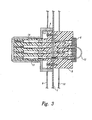
- Figure 3 illustrates one example of a replaced connection.
- a short length of insulated wire 12 installed on the rear insert 5 makes a connection between a contact 13 isolated from the board and another contact 14.
Landscapes
- Engineering & Computer Science (AREA)
- Manufacturing & Machinery (AREA)
- Coupling Device And Connection With Printed Circuit (AREA)
- Multi-Conductor Connections (AREA)
Description
- On airplanes, modular electronic devices are mounted on fixed shelves. The electronic connections between the modular electronic devices are made with interconnecting wire bundles. It has been shown that a printed wiring board (PWB) in place of the interconnecting wire bundles would save weight, space, and cost.
- However, the airplane industry has a history of introducing modifications to electrical wiring in the field. Whereas changes to wire bundles can be made directly in the airplane, making changes (cuts and jumpers) to a PWB cannot. Therefore, PWBs have not replaced wire bundles.
- Traditionally, the connections between modular electronic devices on commercial airplanes have been made with wire bundles. It has been shown that in cases where a series of modular electronic devices are mounted on fixed shelves, a printed wiring board in place of the interconnecting wire bundles would save weight, save space and cost less to produce.
- The airplane industry has a history of introducing modifications to electrical wiring in the field. Airlines perceive changes to printed wiring boards using conventional methods as an obstacle to their use. The confines of the electronics bay of a commercial airplane do not allow the kind of precision work needed for making PWB modifications. The soldering irons needed for adding jumpers is considered hazardous in the flightline environment where fuel vapors are sometimes present.
- Printed wiring boards in combination with wire wrap technology has been proposed as an alternative to pure printed circuits. While this solution offered a good way of adding jumpers, it did not offer practical advantages for making cuts. Wire wrap has also been viewed with disfavor due to its susceptibility to foreign object contamination.
- Once a device with a printed wiring board is designed and built, it is difficult or impossible to change the connectivity of the wiring board in the field in the end product. Making changes to printed wiring boards has traditionally been done by adding "cuts" and "jumpers" to the board. The cut and jumper work is typically only performed in special repair facilities by specially trained technicians using specialized tools. The "cuts" are made by drilling or scraping away the copper trace where the connection is no longer desired. The operation often requires precision in locating the proper trace. The "jumpers" are added by soldering the ends of an insulated wire to the points where a new connection is desired.
- The present invention according to claim 1 allows changes in connectivity to be introduced to a device using only the tools, skills and materials that would be familiar to a mechanic with a background working with wire bundles. Further, the modifications can be done where the printed wiring board is installed instead of a repair facility.
- The present invention enables the use of PWBs to replace interconnecting wire bundles. Therefore, changes in connectivity may be introduced using only tools, skills, and materials familiar to the mechanic instead of the requirement of a repair facility.
- A novel connector assembly is hereinafter described. The present connector assembly contains special contact providing three connections. The front end of the contact mates with the connector for a modular electronic device. The rear end can accept a wired contact for making additional connections not contained in the PWB. The middle section of the contact makes a compliant connection to the board. Additionally, a signal can be disconnected from the PWB by removing the contact and replacing it with a contact that is insulated from the PWB. Thus, the present invention allows the opening of an existing connection, adding a connection, or replacing a connection.
- A hereinafter described embodiment of the present invention comprises a connector with a double ended pin contact with compliant section, a double ended pin contact with an insulated section, and the flexibility of adding connecting wires to any contact in the connector using a rear insert.
-
- Harting et al., U.S. Patent No. 5,509,823 - "Electrical Mating Connector"
This patent relates to a shielding technique for a connector. - Fiori et at., U.S. Patent No. 5,312,265 - "Electrical Connector Suitable for
Use With Variable Numbers of Electrical Conductors"
This patent relates to a way of keeping a connector sealed from moisture or other contaminants even with empty contact locations. - Yoshino, U.S. Patent No. 5,334,341 "Connector Having
Electromagnetic Shielding Film"
This patent relates to a manner of providing shielding around each individual contact of a connector to prevent crosstalk between pins. - Benasutti, U.S. Patent No. 4,530,551 "Circuit Change Pin for Printed
Wiring Board"
The purpose of this patent which is considered as closest prior art, is to make a change to a printed circuit backplane using an elongated connector contact that is insulated from the printed wiring board plated through hole. The contact in this patent is in two pieces. It appears that the two-piece contact would require access to both sides of the printed circuit board. The present one-piece contact can be installed with access to only one side of the board. - Zaderej, U.S. Patent No. 5,127,949 "Plated Electrical Connectors"
This patent involves forming electrical connectors as an integral part of the manufacture of a printed wiring board. - Paulas, U.S. Patent No. 5,257,949 "Connector with Interchangeable
Contacts"
This patent covers a sophisticated type of filter connector with provisions for different types of filter contacts and transient suppression contacts. - Marolda, U.S. Patent No. 4,909,751 "Underwater Mateable
Electrical Connector"
This patent covers an electrical connector that can be mated while it is submerged in water. - Marolda, U.S. Patent No. 4,874,326 "Elastomeric Electrical Isolation
Membrane"
This patent relates to an underwater connector. - Benasutti, U.S. Patent No. 4,418,326 "Electrical Connector for
Printed Wiring Board"
This patent covers a soldered connector that can be disassembled to allow cleaning and replacement of damaged contacts. -
-
- Fig. 1 is a cut-away view of a preferred embodiment of the present system for modifying printed wiring connectors;
- Fig. 2 is illustrative of the present system with the connector shell and connector insert removed and illustrates the sequence of removing the double-ended connector pin contact hereinafter described; and
- Fig. 3 is illustrative of a replaced connection.
-
- The printed wiring board 1 contains copper traces that carry electrical signals between the plated through holes. The plated through holes are where electrical connections are made between the traces and connector contacts.
- The double-ended connector pin contact with compliant section 2 makes an electrical connection between the device that mates with the connector and the plated through hole in the printed wiring board. The contact is not soldered in place. Prior to insertion, the diameter of the compliant section is larger than the diameter of the plated through hole. When the contact is installed, the compliant section is under compression in the plated through hole creating a physical, gas tight, electrical connection to the plated through hole. The contact extends through the plated through hole to form a second mating interface on the far side of the printed wiring board. The end of the contact on the far side of the printed wiring board is used as a connection node for wires added as part of a connection modification.
- The double-ended connector pin contact with
insulated section 3 electrically isolates the contact from the plated through hole in the printed wiring board 1. The contact has, in place of a compliant section, an insulated sleeve that prevents electrical conduction with the plated through hole. The contact extends through the plated through hole to form a second mating interface on the far side of the printed wiring board. The end of the contact on the far side of the printed wiring board is used as a connection node for wires added as part of a connection modification. - The bottom insert 4 and the connector insert 7 and the
contacts 2,and 3 are installed as an assembly into the printed wiring board. The bottom insert 4 and the connector insert 7 captures the contacts as an insert set. The bottom insert 4 prevents the contacts from being forced through the printed wiring board by a miss-aligned mating contact. - The connector insert 7 holds the double-ended connector pin contact in place and it is also used as a mass insertion tool. Force applied by a press to the front of the insert is transferred to the contacts through the insert and forces the compliant sections into the plated through holes.
- The rear insert 5 captivates the mating socket contact of a jumper wire that connects to the extended portion of the double-ended connector pin contact.
- The rubber grommet 6 (part of the rear insert) provides wire support and some protection of the contact area inside the rear insert from foreign objects and moisture.
- The connector shell 8 (mounting fasteners are not shown) captivates the connector insert and provides the rugged mechanical interface required to interface to a modular electronic device.
- The front housing 9 and the
rear housing 10 are metal covers that protect the assembly from foreign objects and provide additional stiffness to the assembly. - Remove fasteners (not shown) from the connector shell 8 and remove the shell. Slide the connector insert 7 off of the double-ended connector pin contacts 2. Figure 2 shows the system with the connector shell and connector insert removed. It illustrates the sequence of removing a double-ended connector pin contact 2 described next.
- Slide the hollow shaft of the
contact removal tool 11 over the end of the double-ended connector pin contact. - The
contact removal tool 11 grabs the ledge of the largest diameter of the contact such that when a force is applied to the tool away from the printed wiring board the contact is extracted from the printed wiring board. Remove the contact from the contact removal tool by pushing the contact further into the shaft until it falls out the other end of the shaft near the handle. - Slide the connector insert 7 over the double-ended connector contacts 2 that remain installed. Fasten the connector shell over the connector insert.
- Prepare a wire of sufficient length terminated to a MIL-C-39029 or similar socket contact. Using a MIL-I-81969 or similar wire insertion tool, insert one end of the prepared wire through the rubber grommet 6 of the rear insert 5 at the location of the contact carrying the desired signal. Using the same insertion tool, insert the other end of the prepared wire through the rubber grommet of the rear insert at the location of the contact that is to receive the signal.
- There are often cases where a signal must be disconnected from the plated through hole on the printed wiring board but a connection must also be added. In this case the following steps are used:
- Remove fasteners (not shown) from the connector shell 8 and remove the shell. Slide the connector insert 7 off of the double-ended connector pin contacts 2. Slide the hollow shaft of the
contact removal tool 11 over the end of the double-ended connector pin contact 2. Pull the tool back away from the printed wiring board thereby removing the contact as described in Opening a Connection and as shown in Fig. 2. In place of the removed contact, install a double-ended connector pin contact withinsulated section 3. The contact will slide into place. Slide the connector insert over the double-ended connector pin contacts. Fasten the connector shell over the connector insert. Add a connection with a wire as described in Adding a Connection. - Figure 3 illustrates one example of a replaced connection. A short length of
insulated wire 12 installed on the rear insert 5 makes a connection between acontact 13 isolated from the board and anothercontact 14. - Modifying connections using the aforementioned system accomplishes what cuts and jumpers accomplish in conventional printed wiring board systems except it:
- Does not require precision removal of conductive material;
- Does not require soldering devices and drills; and
- Uses the type of tools and techniques currently in use in field service of airplanes.
- Unique features of the present invention include:
- Connector contacts that can be removed with minor disassembly of the connector;
- A double-ended connector pin contact having a compliant section;
- A double-ended connector pin contact having an insulated section; and
- Connecting wires can be added to any signal carried in the connector using the rear insert.
Claims (7)
- A connector assembly comprising:(a) a printed wiring board (1) having a first side and second side, and plurality of copper-plated holes therein;(b) a plurality of individually removable, elongated contact pins engaged and electrically connected with the holes in the printed wiring board by way of a compliant middle section (2), and adapted on one end thereof for contact with single wire socket contact devices;(c) a connector insert (7) positioned on the first side of the printed wiring board and having holes therein extending from one side of the insert to the other, adapted for receiving one end of the pins through one side thereof, and for connecting the pins to a modular electronic device connector on the other;(d) a rear insert (5) positioned on the second side of the printed wiring board, having holes therein adapted for receiving the other end of the pins through one side thereof and wherein a MIL-I-81969 or similar wire insertion tool is insertable from the other side.
- The connector assembly of claim 1 wherein the rear insert is comprised of an insulating material and contains clips along the inner periphery of the holes to releasably secure the socket contact devices.
- The connector assembly of claim 1 or 2 that additionally comprises a jumper wire (12) having socket contact devices on both ends thereof, providing an electrical connection between two contact pins on the rear insert side of the assembly.
- The connector assembly of claim 1, 2 or 3 that additionally comprises an elongated pin positioned in one of the holes of the board, the pin having an insulating sleeve (3) that prevents a electrical signal from being transmitted between the pin and the board.
- The connector assembly of any of claims 1-4 wherein the profile of the inner periphery of the holes in the connector insert and the profile of the pins are adapted to keep the pins in position when the connector insert is fastened in place.
- The connector assembly of any of claims 1-5 that additionally comprises a bottom insert (4) between the connector insert and the printed wiring board, which prevents the contacts from being forced through the printed wiring board by a miss-aligned mating contact, and the profile of the pins and the inner periphery of the holes in the bottom insert are adapted to provide a stop for pins on insertion the printed wiring board.
- The connector assembly of any of claims 1-6 that additionally comprises a connector shell that covers the connector insert.
Applications Claiming Priority (2)
| Application Number | Priority Date | Filing Date | Title |
|---|---|---|---|
| US159321 | 1998-09-23 | ||
| US09/159,321 US6231354B1 (en) | 1998-09-23 | 1998-09-23 | System for modifying printed wiring connections after installation |
Publications (3)
| Publication Number | Publication Date |
|---|---|
| EP0989631A2 EP0989631A2 (en) | 2000-03-29 |
| EP0989631A3 EP0989631A3 (en) | 2002-01-09 |
| EP0989631B1 true EP0989631B1 (en) | 2005-11-02 |
Family
ID=22572068
Family Applications (1)
| Application Number | Title | Priority Date | Filing Date |
|---|---|---|---|
| EP99202726A Expired - Lifetime EP0989631B1 (en) | 1998-09-23 | 1999-08-23 | System for modifying printed wiring connections after installation |
Country Status (5)
| Country | Link |
|---|---|
| US (1) | US6231354B1 (en) |
| EP (1) | EP0989631B1 (en) |
| CN (1) | CN1114970C (en) |
| CA (1) | CA2280322C (en) |
| DE (1) | DE69928058T2 (en) |
Families Citing this family (6)
| Publication number | Priority date | Publication date | Assignee | Title |
|---|---|---|---|---|
| EP1238849B1 (en) * | 2001-03-07 | 2013-05-15 | Continental Automotive GmbH | Instrument panel for a motor vehicle |
| US7121875B2 (en) * | 2003-12-09 | 2006-10-17 | The Boeing Company | Integration area, system and method for providing interconnections among components |
| US7074073B2 (en) * | 2004-01-15 | 2006-07-11 | The Boeing Company | Electrical connector insert and apparatus and associated fabrication method |
| TWM257568U (en) * | 2004-02-18 | 2005-02-21 | Acbel Polytech Inc | A switching device for the single-phase/three-phase power supply |
| US7351115B1 (en) * | 2007-01-17 | 2008-04-01 | International Business Machines Corporation | Method for modifying an electrical connector |
| JP2013114830A (en) * | 2011-11-28 | 2013-06-10 | Tyco Electronics Japan Kk | Waterproof connector, and packaging structure and packaging method of waterproof connector |
Citations (1)
| Publication number | Priority date | Publication date | Assignee | Title |
|---|---|---|---|---|
| US4173387A (en) * | 1978-03-28 | 1979-11-06 | Amp Incorporated | Snap-on pin header |
Family Cites Families (13)
| Publication number | Priority date | Publication date | Assignee | Title |
|---|---|---|---|---|
| US3601750A (en) * | 1970-02-09 | 1971-08-24 | Berg Electronics Inc | Circuit board connector |
| US4017143A (en) * | 1975-12-16 | 1977-04-12 | Litton Systems, Inc. | Solderless electrical contact |
| US4418972A (en) | 1982-02-01 | 1983-12-06 | Burroughs Corporation | Electrical connector for printed wiring board |
| US4619495A (en) * | 1982-09-07 | 1986-10-28 | Sochor Jerzy R | High-density press-fit cardedge connectors |
| US4530551A (en) | 1984-01-12 | 1985-07-23 | Burroughs Corp. | Circuit change pin for printed wiring board |
| FR2582867B1 (en) * | 1985-06-03 | 1990-01-19 | Souriau | ELECTRICAL DISTRIBUTION AND CONNECTION INSTALLATION WITH A LARGE NUMBER OF CONDUCTORS, ESPECIALLY FOR AERONAUTICS |
| US4909751A (en) | 1988-09-20 | 1990-03-20 | The United States Of America As Represented By The Secretary Of The Navy | Underwater mateable electrical connector |
| US4874326A (en) | 1988-09-20 | 1989-10-17 | The United States Of America As Represented By The Secretary Of The Navy | Elastomeric electrical isolation membrane |
| US5127838A (en) | 1990-02-23 | 1992-07-07 | General Electric Company | Plated electrical connectors |
| CA2121347C (en) | 1991-10-17 | 1998-06-23 | Eric James Paulus | Connector with interchangeable contacts |
| JP2910390B2 (en) | 1992-03-31 | 1999-06-23 | 日本電気株式会社 | connector |
| US5312265A (en) | 1992-08-10 | 1994-05-17 | Dow Corning Corporation | Electrical connector suitable for use with variable numbers of electrical conductors |
| DE4341103C1 (en) | 1993-12-02 | 1995-01-12 | Harting Elektronik Gmbh | Electrical plug connector |
-
1998
- 1998-09-23 US US09/159,321 patent/US6231354B1/en not_active Expired - Lifetime
-
1999
- 1999-08-13 CA CA002280322A patent/CA2280322C/en not_active Expired - Lifetime
- 1999-08-23 DE DE69928058T patent/DE69928058T2/en not_active Expired - Lifetime
- 1999-08-23 EP EP99202726A patent/EP0989631B1/en not_active Expired - Lifetime
- 1999-09-21 CN CN99120345A patent/CN1114970C/en not_active Expired - Lifetime
Patent Citations (1)
| Publication number | Priority date | Publication date | Assignee | Title |
|---|---|---|---|---|
| US4173387A (en) * | 1978-03-28 | 1979-11-06 | Amp Incorporated | Snap-on pin header |
Also Published As
| Publication number | Publication date |
|---|---|
| DE69928058T2 (en) | 2006-07-13 |
| CA2280322A1 (en) | 2000-03-23 |
| CN1114970C (en) | 2003-07-16 |
| EP0989631A2 (en) | 2000-03-29 |
| DE69928058D1 (en) | 2005-12-08 |
| US6231354B1 (en) | 2001-05-15 |
| CN1248802A (en) | 2000-03-29 |
| CA2280322C (en) | 2002-07-02 |
| EP0989631A3 (en) | 2002-01-09 |
Similar Documents
| Publication | Publication Date | Title |
|---|---|---|
| US4179172A (en) | Modular hardware packaging apparatus | |
| US4548453A (en) | Right angle coaxial plug connector | |
| US4597631A (en) | Printed circuit card hybrid | |
| US4418972A (en) | Electrical connector for printed wiring board | |
| US3551874A (en) | Multiple coaxial connector | |
| US4782245A (en) | Connecting and switching apparatus with selectable connections | |
| US4702707A (en) | Power contact having removable mating components | |
| US4053199A (en) | Cable connectable bulkhead filter array | |
| US5010446A (en) | Multi-edge extender board | |
| EP0308092A2 (en) | Cable shield termination for an electrical connector | |
| EP1221829A2 (en) | Segmented replaceable backplane system for electronic apparatus | |
| US6390829B1 (en) | Electrical connector assembly for a printed circuit board | |
| EP0260967B1 (en) | Connector with compliant retainer | |
| EP0152743A1 (en) | Modular electrical connector | |
| US6231354B1 (en) | System for modifying printed wiring connections after installation | |
| EP0522798A3 (en) | Electrical connector | |
| US6086388A (en) | Auxiliary switch system for use with removable circuit breaker | |
| EP3776749B1 (en) | Longitudinally expandable electrical connector | |
| US3649956A (en) | Replaceable electrical connector | |
| CA1163376A (en) | Modular connector assembly having an electrical contact | |
| EP0643448A1 (en) | Coaxial connector for connection to a printed circuit board | |
| US4695923A (en) | Printed circuit board bolt-on power distribution system | |
| JPH09214154A (en) | Rack for automatic insertion and removal method electronic circuit board, rack and cabinet thereof, and method for removing electronic circuit board | |
| EP1115182A1 (en) | Cable connector for a shielded cable | |
| WO1999030389A1 (en) | Connector |
Legal Events
| Date | Code | Title | Description |
|---|---|---|---|
| PUAI | Public reference made under article 153(3) epc to a published international application that has entered the european phase |
Free format text: ORIGINAL CODE: 0009012 |
|
| AK | Designated contracting states |
Kind code of ref document: A2 Designated state(s): AT BE CH CY DE DK ES FI FR GB GR IE IT LI LU MC NL PT SE Kind code of ref document: A2 Designated state(s): DE FR GB |
|
| AX | Request for extension of the european patent |
Free format text: AL;LT;LV;MK;RO;SI |
|
| PUAL | Search report despatched |
Free format text: ORIGINAL CODE: 0009013 |
|
| AK | Designated contracting states |
Kind code of ref document: A3 Designated state(s): AT BE CH CY DE DK ES FI FR GB GR IE IT LI LU MC NL PT SE |
|
| AX | Request for extension of the european patent |
Free format text: AL;LT;LV;MK;RO;SI |
|
| RIC1 | Information provided on ipc code assigned before grant |
Free format text: 7H 01R 29/00 A |
|
| 17P | Request for examination filed |
Effective date: 20020124 |
|
| AKX | Designation fees paid |
Free format text: DE FR GB |
|
| 17Q | First examination report despatched |
Effective date: 20030602 |
|
| GRAP | Despatch of communication of intention to grant a patent |
Free format text: ORIGINAL CODE: EPIDOSNIGR1 |
|
| GRAS | Grant fee paid |
Free format text: ORIGINAL CODE: EPIDOSNIGR3 |
|
| GRAA | (expected) grant |
Free format text: ORIGINAL CODE: 0009210 |
|
| AK | Designated contracting states |
Kind code of ref document: B1 Designated state(s): DE FR GB |
|
| REG | Reference to a national code |
Ref country code: GB Ref legal event code: FG4D |
|
| REF | Corresponds to: |
Ref document number: 69928058 Country of ref document: DE Date of ref document: 20051208 Kind code of ref document: P |
|
| ET | Fr: translation filed | ||
| PLBE | No opposition filed within time limit |
Free format text: ORIGINAL CODE: 0009261 |
|
| STAA | Information on the status of an ep patent application or granted ep patent |
Free format text: STATUS: NO OPPOSITION FILED WITHIN TIME LIMIT |
|
| 26N | No opposition filed |
Effective date: 20060803 |
|
| REG | Reference to a national code |
Ref country code: FR Ref legal event code: PLFP Year of fee payment: 18 |
|
| REG | Reference to a national code |
Ref country code: FR Ref legal event code: PLFP Year of fee payment: 19 |
|
| REG | Reference to a national code |
Ref country code: FR Ref legal event code: PLFP Year of fee payment: 20 |
|
| PGFP | Annual fee paid to national office [announced via postgrant information from national office to epo] |
Ref country code: DE Payment date: 20180829 Year of fee payment: 20 Ref country code: FR Payment date: 20180827 Year of fee payment: 20 |
|
| PGFP | Annual fee paid to national office [announced via postgrant information from national office to epo] |
Ref country code: GB Payment date: 20180828 Year of fee payment: 20 |
|
| REG | Reference to a national code |
Ref country code: DE Ref legal event code: R071 Ref document number: 69928058 Country of ref document: DE |
|
| REG | Reference to a national code |
Ref country code: GB Ref legal event code: PE20 Expiry date: 20190822 |
|
| PG25 | Lapsed in a contracting state [announced via postgrant information from national office to epo] |
Ref country code: GB Free format text: LAPSE BECAUSE OF EXPIRATION OF PROTECTION Effective date: 20190822 |