EP0989547A2 - "Thin-film magnetic head device" - Google Patents
"Thin-film magnetic head device" Download PDFInfo
- Publication number
- EP0989547A2 EP0989547A2 EP99202412A EP99202412A EP0989547A2 EP 0989547 A2 EP0989547 A2 EP 0989547A2 EP 99202412 A EP99202412 A EP 99202412A EP 99202412 A EP99202412 A EP 99202412A EP 0989547 A2 EP0989547 A2 EP 0989547A2
- Authority
- EP
- European Patent Office
- Prior art keywords
- magnetic
- layer
- head device
- soft
- thin
- Prior art date
- Legal status (The legal status is an assumption and is not a legal conclusion. Google has not performed a legal analysis and makes no representation as to the accuracy of the status listed.)
- Withdrawn
Links
Images


Classifications
-
- B—PERFORMING OPERATIONS; TRANSPORTING
- B82—NANOTECHNOLOGY
- B82Y—SPECIFIC USES OR APPLICATIONS OF NANOSTRUCTURES; MEASUREMENT OR ANALYSIS OF NANOSTRUCTURES; MANUFACTURE OR TREATMENT OF NANOSTRUCTURES
- B82Y25/00—Nanomagnetism, e.g. magnetoimpedance, anisotropic magnetoresistance, giant magnetoresistance or tunneling magnetoresistance
-
- B—PERFORMING OPERATIONS; TRANSPORTING
- B82—NANOTECHNOLOGY
- B82Y—SPECIFIC USES OR APPLICATIONS OF NANOSTRUCTURES; MEASUREMENT OR ANALYSIS OF NANOSTRUCTURES; MANUFACTURE OR TREATMENT OF NANOSTRUCTURES
- B82Y10/00—Nanotechnology for information processing, storage or transmission, e.g. quantum computing or single electron logic
-
- G—PHYSICS
- G11—INFORMATION STORAGE
- G11B—INFORMATION STORAGE BASED ON RELATIVE MOVEMENT BETWEEN RECORD CARRIER AND TRANSDUCER
- G11B5/00—Recording by magnetisation or demagnetisation of a record carrier; Reproducing by magnetic means; Record carriers therefor
- G11B5/127—Structure or manufacture of heads, e.g. inductive
- G11B5/33—Structure or manufacture of flux-sensitive heads, i.e. for reproduction only; Combination of such heads with means for recording or erasing only
- G11B5/332—Structure or manufacture of flux-sensitive heads, i.e. for reproduction only; Combination of such heads with means for recording or erasing only using thin films
-
- G—PHYSICS
- G11—INFORMATION STORAGE
- G11B—INFORMATION STORAGE BASED ON RELATIVE MOVEMENT BETWEEN RECORD CARRIER AND TRANSDUCER
- G11B5/00—Recording by magnetisation or demagnetisation of a record carrier; Reproducing by magnetic means; Record carriers therefor
- G11B5/127—Structure or manufacture of heads, e.g. inductive
- G11B5/33—Structure or manufacture of flux-sensitive heads, i.e. for reproduction only; Combination of such heads with means for recording or erasing only
- G11B5/39—Structure or manufacture of flux-sensitive heads, i.e. for reproduction only; Combination of such heads with means for recording or erasing only using magneto-resistive devices or effects
- G11B5/3903—Structure or manufacture of flux-sensitive heads, i.e. for reproduction only; Combination of such heads with means for recording or erasing only using magneto-resistive devices or effects using magnetic thin film layers or their effects, the films being part of integrated structures
- G11B5/3906—Details related to the use of magnetic thin film layers or to their effects
- G11B5/3909—Arrangements using a magnetic tunnel junction
-
- G—PHYSICS
- G11—INFORMATION STORAGE
- G11B—INFORMATION STORAGE BASED ON RELATIVE MOVEMENT BETWEEN RECORD CARRIER AND TRANSDUCER
- G11B5/00—Recording by magnetisation or demagnetisation of a record carrier; Reproducing by magnetic means; Record carriers therefor
- G11B5/127—Structure or manufacture of heads, e.g. inductive
- G11B5/33—Structure or manufacture of flux-sensitive heads, i.e. for reproduction only; Combination of such heads with means for recording or erasing only
- G11B5/39—Structure or manufacture of flux-sensitive heads, i.e. for reproduction only; Combination of such heads with means for recording or erasing only using magneto-resistive devices or effects
- G11B5/3903—Structure or manufacture of flux-sensitive heads, i.e. for reproduction only; Combination of such heads with means for recording or erasing only using magneto-resistive devices or effects using magnetic thin film layers or their effects, the films being part of integrated structures
- G11B5/3906—Details related to the use of magnetic thin film layers or to their effects
- G11B5/3916—Arrangements in which the active read-out elements are coupled to the magnetic flux of the track by at least one magnetic thin film flux guide
- G11B5/3919—Arrangements in which the active read-out elements are coupled to the magnetic flux of the track by at least one magnetic thin film flux guide the guide being interposed in the flux path
-
- G—PHYSICS
- G11—INFORMATION STORAGE
- G11B—INFORMATION STORAGE BASED ON RELATIVE MOVEMENT BETWEEN RECORD CARRIER AND TRANSDUCER
- G11B5/00—Recording by magnetisation or demagnetisation of a record carrier; Reproducing by magnetic means; Record carriers therefor
- G11B5/127—Structure or manufacture of heads, e.g. inductive
- G11B5/33—Structure or manufacture of flux-sensitive heads, i.e. for reproduction only; Combination of such heads with means for recording or erasing only
- G11B5/39—Structure or manufacture of flux-sensitive heads, i.e. for reproduction only; Combination of such heads with means for recording or erasing only using magneto-resistive devices or effects
- G11B5/3903—Structure or manufacture of flux-sensitive heads, i.e. for reproduction only; Combination of such heads with means for recording or erasing only using magneto-resistive devices or effects using magnetic thin film layers or their effects, the films being part of integrated structures
- G11B5/3906—Details related to the use of magnetic thin film layers or to their effects
- G11B5/3945—Heads comprising more than one sensitive element
-
- G—PHYSICS
- G11—INFORMATION STORAGE
- G11B—INFORMATION STORAGE BASED ON RELATIVE MOVEMENT BETWEEN RECORD CARRIER AND TRANSDUCER
- G11B5/00—Recording by magnetisation or demagnetisation of a record carrier; Reproducing by magnetic means; Record carriers therefor
- G11B5/127—Structure or manufacture of heads, e.g. inductive
- G11B5/33—Structure or manufacture of flux-sensitive heads, i.e. for reproduction only; Combination of such heads with means for recording or erasing only
- G11B5/39—Structure or manufacture of flux-sensitive heads, i.e. for reproduction only; Combination of such heads with means for recording or erasing only using magneto-resistive devices or effects
- G11B2005/3996—Structure or manufacture of flux-sensitive heads, i.e. for reproduction only; Combination of such heads with means for recording or erasing only using magneto-resistive devices or effects large or giant magnetoresistive effects [GMR], e.g. as generated in spin-valve [SV] devices
-
- G—PHYSICS
- G11—INFORMATION STORAGE
- G11B—INFORMATION STORAGE BASED ON RELATIVE MOVEMENT BETWEEN RECORD CARRIER AND TRANSDUCER
- G11B5/00—Recording by magnetisation or demagnetisation of a record carrier; Reproducing by magnetic means; Record carriers therefor
- G11B5/127—Structure or manufacture of heads, e.g. inductive
- G11B5/187—Structure or manufacture of the surface of the head in physical contact with, or immediately adjacent to the recording medium; Pole pieces; Gap features
- G11B5/245—Structure or manufacture of the surface of the head in physical contact with, or immediately adjacent to the recording medium; Pole pieces; Gap features comprising means for controlling the reluctance of the magnetic circuit in a head with single gap, for co-operation with one track
Definitions
- the present invention relates to a thin-film magnetic read head device comprising an end face extending in a first direction, in which a magnetic information carrier is movable with respect to the magnetic head device, and in a second direction, perpendicular to said first direction, the magnetic head device further comprising a multilayer structure with at least two soft-magnetic layers separated by a magnetic insulation layer and with at least one exchange biasing layer cooperating with one of said soft-magnetic layers, which multilayer structure extends in the second direction and in a third direction, perpendicular to the first and the second direction, and forms at least one flux path in the first and the third direction.
- Such a thin-film magnetic read head device is known from Koshkawa et al, Flux-Guided MR Head for Very Low Hying Height, IEEE Trans. Magn. 30 (1994), pp. 3840-3842.
- a shielded read head is described and illustrated with an interrupted wing-like exchange biasing layer, the interruption determining the read width.
- the wing-like embodiment of the exchange biasing layer is applied for stabilizing a magnetoresistive element by boundary control stabilization and for determining the read width.
- this magnetic read head device is not appropriate to realize read widths below about 1 ⁇ m.
- the dimension in the second direction of the flux guide in front of a magnetoresistive element usually determined the read width.
- a multichannel magnetic read head device was obtained by an arrangement in the second direction of flux guides and magnetoresistive elements cooperating therewith.
- multidomain states were likely to occur in the front flux guide, resulting in Barkhausen noise. Therefore an improvement was proposed in PHN 16.062 EP-P.
- this document describes a number of flux-guiding elements and a number of magnetoresistive elements, cooperating with said flux-guiding elements, which elements form a number of parallel flux paths in the first and the third direction, the number corresponding to the number of magnetic channels of the magnetic read head device.
- a channel separation i.e. a separation of the parallel flux pats, is obtained by a magnetically anisotropic structure, the magnetic permeability thereof in the second direction being small in comparison with the magnetic permeability in the third direction.
- the read widths are controlled by the anisotropy in combination with the distance between the contacts on the magnetoresistive elements.
- This method allows use of front flux guides with a width larger than the read width and thereby retains a single domain configuration also for smaller track widths. This is a viable method for track widths down to about 5 ⁇ m. For track widths of a few microns and less, this method appears to be no longer sufficient due to limitations in the soft-magnetic material properties.
- the read width was determined by the spacing between the contacts on the magnetoresistive element or, in the case of a multichannel head, magnetoresistive elements.
- a thin-film magnetic read head device as described in the opening paragraph, which is characterized in that the exchange coupling between one of the soft-magnetic layers and the exchange biasing layer is at least partly reduced locally in at least the second direction, and in that the exchange biasing layer extends uninterruptedly in the region of said local reductions.
- the expression “reduced” means “interrupted or at least substantially reduced”
- the expression “reduction” means “interruption of or at least substantial reduction”.
- a locally reduced exchange coupling between one of the soft-magnetic layers and the exchange biasing layer may be important to control the read width as well as the flux-guiding efficiency.
- an exchange biasing layer of such a type is excluded from the term exchange biasing layer in the sense of the present invention in which the coupling between the exchange biasing layer and the adjacent soft-magnetic layer is locally reduced to control the read width or to improve the flux-guiding efficiency.
- the present invention can be applied in shielded type magnetic heads as well as in yoke-type magnetic read heads. In both cases, a small-sized read width for a magnetic read head device will be obtained by applying the idea of local reduction of the coupling between an uninterrupted exchange biasing layer and a soft-magnetic layer.
- the exchange biasing layer may not only be provided on one of the soft-magnetic layers, but may also be constituted by or be part of the magnetic insulation layer. In a configuration with two exchange biasing layers, both situations may occur.
- the reduction can be achieved by the introduction of a specific interface layer structure, particularly only a few monolayers, of non-magnetic material between the exchange biasing layer and the soft-magnetic layer.
- a specific interface layer structure particularly only a few monolayers, of non-magnetic material between the exchange biasing layer and the soft-magnetic layer.
- the thickness and/or the composition or microstructure of the interface layer between the exchange biasing layer and the soft-magnetic adjacent layer is locally modified, e.g. by in situ focused ion beam etching or implantation.
- At least one magnetoresistive element which may comprise at least one of said soft-magnetic layers and said exchange biasing layer, the exchange biasing between these layers at least being partly reduced locally to control the read width.
- the at least one magnetoresistive element may also be magnetically coupled with or comprise the soft-magnetic layer which is locally coupled with the exchange biasing layer to control the read width.
- the soft-magnetic layer to which the magnetoresistive element is magnetically coupled may be interrupted in the third direction, while the exchange coupling of the part of said interrupted soft-magnetic layer which is most near the end face and the exchange biasing layer is locally reduced to control the read width.
- an exchange biasing layer may be provided between the magnetoresistive element and the soft-magnetic layer to which the magnetoresistive element is coupled, with the exchange biasing being decoupled in the contact region of the magnetoresistive element with the latter exchange biasing layer to control the flux-guiding to said magnetoresistive element.
- the magnetoresistive element may be of an anisotropic (AMR), a giant (GMR) or a spin tunnel junction (STJ-MR) type.
- AMR anisotropic
- GMR giant
- STJ-MR spin tunnel junction
- the magnetic read head device is a multichannel magnetic head device with the soft-magnetic layers and a number of magnetoresistive elements forming a corresponding number of parallel flux paths in the first and the third direction, this number corresponding to the number of magnetic channels of the magnetic head device.
- the invention not only relates to a thin-film magnetic head device as indicated above, but also relates to a system for recording and/or reproducing information, comprising such a thin-film magnetic head device.
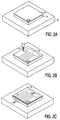
- a shielded read head incorporates successively a first flux-guiding element in the form of a lower shield layer 1 on a substrate 2, a first gap layer 3, a magnetoresistive element in the form of a soft adjacent layer magnetoresistive (SAL-MR) structure 4, a second gap layer 5 and a second flux-guiding element in the form of an upper shield 6.
- An exchange biasing layer is part of the lower gap layer 3 or forms this gap layer.
- the exchange biasing material when used with an anisotropic magnetoresistive (AMR) or a giant magnetorisistive (GMR) element, it may be constituted by an electrically non-conductive (antiferromagnetic) exchange biasing material like NiO.
- AMR anisotropic magnetoresistive
- GMR giant magnetorisistive
- the Ni-Fe layer is exchange-coupled (magnetically pinned) to the exchange biasing layer outside the reading area 8.
- Contacts 9 and 10 are provided between the SAL-MR layer structure outside the reading area and the gap layer 5.
- the location of the contacts on the SAL-MR layer structure will not influence the read width as long as they are in the area where the magnetization is fixed, i.e. outside the reading area. However, a location not too far from the sensing region, i.e. the reading area, will be preferred for an optimal response.
- the voltage across the contact leads 9 and 10 represents the read magnetic information from an information carrier moved along this shielded magnetic head device.
- the exchange biasing layer stabilizes the SAL-MR layer structure also in the longitudinal direction.
- the shielded AMR head is polished, as indicated in Fig. 1e.
- the read width of the obtained head is determined by the dimension in the second direction of the read area 8.
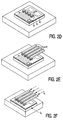
- a multichannel STJ yoke-type read head incorporates successively a first flux-guiding layer 11 on a substrate 12 and an exchange biasing layer in the form of an antiferromagnetic (AF) layer 13.
- AF antiferromagnetic
- a thin dielectric or metal decoupling layer can be introduced between these layers. If the flux-guiding layer 11 is about several microns thick, a decoupling layer is optional because the flux-guiding layer will still have a sufficiently high permeability.
- the exchange biasing layer 13 is in situ implanted with Ga ions by means of focused ion beam implantation (see 14). The implanted surface is indicated by 15. Thereafter (Fig. 2c), an upper flux guide layer 16 is formed, the exchange coupled (magnetically pinned) regions forming separations between parallel flux-guiding paths 17.
- STJ structures are formed as illustrated in Fig. 2d. Each of these structures comprises successively a tunnel barrier layer 18, a pinned STJ layer 19 and a second exchange biasing layer 20.
- the layers 18-20 are provided and the total stack must be structured by an etching process which stops on the tunnel barrier. By this etching process, the individual channels are definitively obtained.
- the upper flux guide layer 16 with the layers 18-20 jointly constitute an STJ-MR element at the top of which contact leads 21 are provided.
- STJs Spin Tunnel Junctions
- the electrical resistance in the vertical direction thereof is dependent on the relative orientation of the magnetization vectors in the decoupled pans of the upper flux layer 16 and the pinned STJ layer 19.
- a sensing current applied to the contact leads 21 results in voltage values which are indicative of the detected magnetic flux by the read head.
- the read width and the accuracy of the read channels are determined by the focused ion beam implantation resulting in the required channel separation.
- the exchange biasing layer controls the read width but also serves as (part of) the read gap.
- a bias current can be applied through the lower flux-guide layer to control the direction of magnetization in the free layer 16 of the STJ.
- the free layer 16 of the STJ also serves as a flux guide.
- the thickness of the free STJ layer annex flux guide 16 should be sufficiently thin to allow a good exchange pinning and sufficiently thick to allow flux transport to the STJ region without significant flux crossing to the lower flux layer 11. This means that the thickness should be in the range of 0,1-5 ⁇ m for the lower flux layer 11 and 0,01-1 ⁇ m for the upper flux guide 16.
- a flux-guided STJ-MR head has the advantage that the junction area is not exposed at the head surface and no shorting across the thin tunnel barrier can occur during contact with the recording medium. Furthermore, the dimensions of the STJ area are less critical because the read width is controlled by the exchange coupling.
- the invention is not limited to the described embodiments but relates to all types of magnetic read heads based on exchange coupling controlled read widths; they may be applied for very high density hard disc recording as well as for advanced tape recording systems.
Abstract


Description
Claims (11)
- A thin-film magnetic read head device comprising an end face extending in a first direction, in which a magnetic information carrier is movable with respect to the magnetic head device, and in a second direction, perpendicular to said first direction, the magnetic head device further comprising a multilayer structure with at least two soft-magnetic layers separated by a magnetic insulation layer and with at least one exchange biasing layer cooperating with one of said soft-magnetic layers, which multilayer structure extends in the second direction and in a third direction, perpendicular to the first and the second direction, and forms at least one flux path in the first and the third direction, characterized in that the exchange coupling between one of the soft-magnetic layers and the exchange biasing layer is at least partly reduced locally in at least the second direction, and in that the exchange biasing layer extends uninterruptedly in the region of said local reductions.
- A thin-film magnetic read head device as claimed in to claim 1, characterized in that the exchange biasing layer is constituted by or forms part of the magnetic insulation layer.
- A thin-film magnetic read head device as claimed in claim 1 or 2, characterized in that an interface layer of a non-magnetic material with a specific structure to control the read width is provided between the exchange biasing layer and a respective soft-magnetic adjacent layer.
- A thin-film magnetic read head device as claimed in claim 3, characterized in that, in accordance with said specific structure, the thickness and/or the composition or microstructure of the interface layer between the exchange biasing layer and the soft-magnetic adjacent layer is locally modified by in situ focused ion beam etching or implantation.
- A thin-film magnetic read head device as claimed in any one of the preceding claims, characterized in that there is provided at least one magnetoresistive element comprising at least one of said soft-magnetic layers and said exchange biasing layer, the exchange biasing between these layers at least being partly reduced locally to control the read width.
- A thin-film magnetic read head device as claimed in any one of claims 1-4, characterized in that there is provided at least one magnetoresistive element which is magnetically coupled with or comprises the soft-magnetic layer which is locally coupled with the exchange biasing layer to control the read width.
- A thin-film magnetic read head device as claimed in claim 6, characterized in that the soft-magnetic layer to which the magnetoresistive element is magnetically coupled is interrupted in the third direction, and in that the exchange coupling of a part of said interrupted soft-magnetic layer which is most near the end face and the exchange biasing layer is locally reduced to control the read width.
- A thin-film magnetic read head device as claimed in claim 7, characterized in that an exchange biasing layer is provided between the magnetoresistive element and the soft-magnetic layer to which the magnetoresistive element is coupled, with the exchange biasing being decoupled in the contact region of the magnetoresistive element with the latter exchange biasing layer to control the flux-guiding to said magnetoresistive element.
- A thin-film magnetic read head device as claimed in claim 6, 7 or 8, characterized in that the magnetoresistive element is of an anisotropic (AMR), a giant (GMR) or a spin tunnel junction (STJ-MR) type.
- A thin-film magnetic read head device as claimed in any one of the claims 4-9, characterized in that the magnetic head device is a multichannel magnetic head device with the soft-magnetic layers and a number of magnetoresistive elements forming a corresponding number of parallel flux paths in the first and the third direction, this number corresponding to the number of magnetic channels of the magnetic head device.
- A system for recording information, comprising a thin-film magnetic read head device as claimed in any one of the preceding claims.
Priority Applications (1)
| Application Number | Priority Date | Filing Date | Title |
|---|---|---|---|
| EP99202412A EP0989547A3 (en) | 1998-07-31 | 1999-07-22 | "Thin-film magnetic head device" |
Applications Claiming Priority (3)
| Application Number | Priority Date | Filing Date | Title |
|---|---|---|---|
| EP98202584 | 1998-07-31 | ||
| EP98202584 | 1998-07-31 | ||
| EP99202412A EP0989547A3 (en) | 1998-07-31 | 1999-07-22 | "Thin-film magnetic head device" |
Publications (2)
| Publication Number | Publication Date |
|---|---|
| EP0989547A2 true EP0989547A2 (en) | 2000-03-29 |
| EP0989547A3 EP0989547A3 (en) | 2005-09-28 |
Family
ID=26150589
Family Applications (1)
| Application Number | Title | Priority Date | Filing Date |
|---|---|---|---|
| EP99202412A Withdrawn EP0989547A3 (en) | 1998-07-31 | 1999-07-22 | "Thin-film magnetic head device" |
Country Status (1)
| Country | Link |
|---|---|
| EP (1) | EP0989547A3 (en) |
Citations (7)
| Publication number | Priority date | Publication date | Assignee | Title |
|---|---|---|---|---|
| EP0326741A2 (en) * | 1988-02-05 | 1989-08-09 | Seagate Technology International | Unbiased single magneto-resistive element ganged read head sensor |
| US5329413A (en) * | 1992-01-10 | 1994-07-12 | Kabushiki Kaisha Toshiba | Magnetoresistance sensor magnetically coupled with high-coercive force film at two end regions |
| US5461526A (en) * | 1992-03-24 | 1995-10-24 | Hitachi, Ltd. | Magnetoresistive read head and magnetic storage system using the same |
| US5461527A (en) * | 1991-09-30 | 1995-10-24 | Kabushiki Kaisha Toshiba | Magneto-resistive head |
| US5668685A (en) * | 1992-02-26 | 1997-09-16 | Hitachi, Ltd. | Magnetic disc apparatus |
| JPH09251622A (en) * | 1996-03-18 | 1997-09-22 | Toshiba Corp | Magnetic head |
| WO1997036289A1 (en) * | 1996-03-27 | 1997-10-02 | Philips Electronics N.V. | Magnetic head with uninterrupted flux guide |
-
1999
- 1999-07-22 EP EP99202412A patent/EP0989547A3/en not_active Withdrawn
Patent Citations (7)
| Publication number | Priority date | Publication date | Assignee | Title |
|---|---|---|---|---|
| EP0326741A2 (en) * | 1988-02-05 | 1989-08-09 | Seagate Technology International | Unbiased single magneto-resistive element ganged read head sensor |
| US5461527A (en) * | 1991-09-30 | 1995-10-24 | Kabushiki Kaisha Toshiba | Magneto-resistive head |
| US5329413A (en) * | 1992-01-10 | 1994-07-12 | Kabushiki Kaisha Toshiba | Magnetoresistance sensor magnetically coupled with high-coercive force film at two end regions |
| US5668685A (en) * | 1992-02-26 | 1997-09-16 | Hitachi, Ltd. | Magnetic disc apparatus |
| US5461526A (en) * | 1992-03-24 | 1995-10-24 | Hitachi, Ltd. | Magnetoresistive read head and magnetic storage system using the same |
| JPH09251622A (en) * | 1996-03-18 | 1997-09-22 | Toshiba Corp | Magnetic head |
| WO1997036289A1 (en) * | 1996-03-27 | 1997-10-02 | Philips Electronics N.V. | Magnetic head with uninterrupted flux guide |
Non-Patent Citations (1)
| Title |
|---|
| PATENT ABSTRACTS OF JAPAN vol. 1998, no. 01, 30 January 1998 (1998-01-30) -& JP 09 251622 A (TOSHIBA CORP), 22 September 1997 (1997-09-22) * |
Also Published As
| Publication number | Publication date |
|---|---|
| EP0989547A3 (en) | 2005-09-28 |
Similar Documents
| Publication | Publication Date | Title |
|---|---|---|
| EP0911810B1 (en) | Magnetic tunnel junction devices | |
| US6271998B1 (en) | Thin film shielded magnetic read head device | |
| US6515573B1 (en) | Method and system for providing edge-junction TMR utilizing a hard magnet as a pinned layer | |
| US6445554B1 (en) | Method and system for providing edge-junction TMR for high areal density magnetic recording | |
| US6223420B1 (en) | Method of making a read head with high resistance soft magnetic flux guide layer for enhancing read sensor efficiency | |
| US5898548A (en) | Shielded magnetic tunnel junction magnetoresistive read head | |
| EP0843303B1 (en) | Spin-valve GMR sensor with inbound exchange stabilization | |
| US8027129B2 (en) | Current perpendicular to plane magnetoresistive sensor pre-product with current confining path precursor | |
| US6671139B2 (en) | In-stack longitudinal bias structure for CIP spin valve sensors with bias layer electrically insulated from free layer | |
| US5554265A (en) | Method of making a magnetoresistive sensor | |
| US6690554B2 (en) | Magnetoresistive-effect device with extended AFM layer and method for manufacturing the same | |
| US6411478B1 (en) | Spin tunnel junction recording heads using an edge junction structure with CIP | |
| US6844998B2 (en) | Magnetoresistive sensor capable of narrowing gap and track width | |
| US6510030B1 (en) | Transducing head and method for forming a recessed shield for a transducing head | |
| US7573675B2 (en) | Thin film magnetic head | |
| US6526649B2 (en) | Manufacturing method of magneto-resistive effect type head | |
| US7201947B2 (en) | CPP and MTJ reader design with continuous exchange-coupled free layer | |
| US6718623B2 (en) | Magnetoresistive device and method of manufacturing same, and thin-film magnetic head and method of manufacturing same | |
| US7414816B2 (en) | Planar magnetic thin film head | |
| US6317302B1 (en) | Thin-film magnetic read head with locally reduced exchange coupling | |
| US6985339B2 (en) | Disc drive having electromagnetic biased shieldless CPP reader | |
| EP0989547A2 (en) | "Thin-film magnetic head device" | |
| US6842314B2 (en) | Magnetoresistive device and method of manufacturing same, and thin-film magnetic head and method of manufacturing same | |
| US6583967B2 (en) | Thin-film magnetic head and method of manufacturing same | |
| JP2002353534A (en) | Magnetoresistive effect element, magnetoresistive effect type magnetic sensor, and magnetoresistive effect type magnetic head |
Legal Events
| Date | Code | Title | Description |
|---|---|---|---|
| PUAI | Public reference made under article 153(3) epc to a published international application that has entered the european phase |
Free format text: ORIGINAL CODE: 0009012 |
|
| AK | Designated contracting states |
Kind code of ref document: A2 Designated state(s): AT BE CH CY DE DK ES FI FR GB GR IE IT LI LU MC NL PT SE |
|
| AX | Request for extension of the european patent |
Free format text: AL;LT;LV;MK;RO;SI |
|
| PUAL | Search report despatched |
Free format text: ORIGINAL CODE: 0009013 |
|
| AK | Designated contracting states |
Kind code of ref document: A3 Designated state(s): AT BE CH CY DE DK ES FI FR GB GR IE IT LI LU MC NL PT SE |
|
| AX | Request for extension of the european patent |
Extension state: AL LT LV MK RO SI |
|
| 17P | Request for examination filed |
Effective date: 20060328 |
|
| AKX | Designation fees paid |
Designated state(s): DE FR GB |
|
| 17Q | First examination report despatched |
Effective date: 20061122 |
|
| STAA | Information on the status of an ep patent application or granted ep patent |
Free format text: STATUS: THE APPLICATION IS DEEMED TO BE WITHDRAWN |
|
| 18D | Application deemed to be withdrawn |
Effective date: 20070605 |