EP0988826B1 - Monolithic silicon intra-ocular pressure sensor and manufacturing method therefor - Google Patents
Monolithic silicon intra-ocular pressure sensor and manufacturing method therefor Download PDFInfo
- Publication number
- EP0988826B1 EP0988826B1 EP99306690A EP99306690A EP0988826B1 EP 0988826 B1 EP0988826 B1 EP 0988826B1 EP 99306690 A EP99306690 A EP 99306690A EP 99306690 A EP99306690 A EP 99306690A EP 0988826 B1 EP0988826 B1 EP 0988826B1
- Authority
- EP
- European Patent Office
- Prior art keywords
- silicon
- pressure
- cannula
- fluid
- sensing
- Prior art date
- Legal status (The legal status is an assumption and is not a legal conclusion. Google has not performed a legal analysis and makes no representation as to the accuracy of the status listed.)
- Expired - Lifetime
Links
- 229910052710 silicon Inorganic materials 0.000 title claims description 31
- 239000010703 silicon Substances 0.000 title claims description 31
- XUIMIQQOPSSXEZ-UHFFFAOYSA-N Silicon Chemical compound [Si] XUIMIQQOPSSXEZ-UHFFFAOYSA-N 0.000 title claims description 30
- 230000004410 intraocular pressure Effects 0.000 title claims description 28
- 238000004519 manufacturing process Methods 0.000 title description 4
- 239000012530 fluid Substances 0.000 claims description 28
- 235000012431 wafers Nutrition 0.000 claims description 22
- 239000000523 sample Substances 0.000 claims description 17
- 239000012528 membrane Substances 0.000 claims description 16
- 238000000034 method Methods 0.000 claims description 16
- 238000005530 etching Methods 0.000 claims description 12
- 238000003780 insertion Methods 0.000 claims description 8
- 230000037431 insertion Effects 0.000 claims description 8
- 230000002262 irrigation Effects 0.000 claims description 8
- 238000003973 irrigation Methods 0.000 claims description 8
- KWYUFKZDYYNOTN-UHFFFAOYSA-M Potassium hydroxide Chemical compound [OH-].[K+] KWYUFKZDYYNOTN-UHFFFAOYSA-M 0.000 claims description 7
- 239000004065 semiconductor Substances 0.000 claims description 5
- 230000013011 mating Effects 0.000 claims description 4
- 238000005269 aluminizing Methods 0.000 claims 1
- 210000001508 eye Anatomy 0.000 description 17
- 238000010276 construction Methods 0.000 description 4
- 230000000694 effects Effects 0.000 description 2
- 239000000463 material Substances 0.000 description 2
- 241001631457 Cannula Species 0.000 description 1
- XAGFODPZIPBFFR-UHFFFAOYSA-N aluminium Chemical compound [Al] XAGFODPZIPBFFR-UHFFFAOYSA-N 0.000 description 1
- 229910052782 aluminium Inorganic materials 0.000 description 1
- 230000015572 biosynthetic process Effects 0.000 description 1
- 238000009530 blood pressure measurement Methods 0.000 description 1
- 210000005252 bulbus oculi Anatomy 0.000 description 1
- 238000005755 formation reaction Methods 0.000 description 1
- 208000014674 injury Diseases 0.000 description 1
- 238000001020 plasma etching Methods 0.000 description 1
- 239000007787 solid Substances 0.000 description 1
- 239000000758 substrate Substances 0.000 description 1
- 238000001356 surgical procedure Methods 0.000 description 1
- 230000007704 transition Effects 0.000 description 1
- 230000008733 trauma Effects 0.000 description 1
Images

Classifications
-
- A—HUMAN NECESSITIES
- A61—MEDICAL OR VETERINARY SCIENCE; HYGIENE
- A61B—DIAGNOSIS; SURGERY; IDENTIFICATION
- A61B3/00—Apparatus for testing the eyes; Instruments for examining the eyes
- A61B3/10—Objective types, i.e. instruments for examining the eyes independent of the patients' perceptions or reactions
- A61B3/16—Objective types, i.e. instruments for examining the eyes independent of the patients' perceptions or reactions for measuring intraocular pressure, e.g. tonometers
-
- A—HUMAN NECESSITIES
- A61—MEDICAL OR VETERINARY SCIENCE; HYGIENE
- A61B—DIAGNOSIS; SURGERY; IDENTIFICATION
- A61B2562/00—Details of sensors; Constructional details of sensor housings or probes; Accessories for sensors
- A61B2562/02—Details of sensors specially adapted for in-vivo measurements
- A61B2562/028—Microscale sensors, e.g. electromechanical sensors [MEMS]
-
- A—HUMAN NECESSITIES
- A61—MEDICAL OR VETERINARY SCIENCE; HYGIENE
- A61B—DIAGNOSIS; SURGERY; IDENTIFICATION
- A61B5/00—Measuring for diagnostic purposes; Identification of persons
- A61B5/0002—Remote monitoring of patients using telemetry, e.g. transmission of vital signals via a communication network
- A61B5/0031—Implanted circuitry
Definitions
- the present invention is directed to a monolithic silicon intra-ocular pressure sensor and a method of construction therefor and, more specifically, to a sensing probe having a cannula end portion for insertion into a human eye for irrigation or for sensing the intra-ocular pressure (IOP) fluid in the interior of the eye.
- IOP intra-ocular pressure
- IOP intra-ocular pressure
- Document US4722350 shows an intraocular pressure sensing probe having a cannula end portion for insertion into an eye for irrigation and comprising a pressure sensing probe at the tip.
- Document US5591139 shows needles or cannulas in a monolithic silicon substrate with an integrated microdetector. Implantable eye pressure sensors are also known from DE 44 38 201 and US4922913.
- an intra-ocular pressure (IOP) sensing probe having a cannula end portion for insertion into an eye for irrigation or for sensing the IOP of fluid in the interior of the eye comprising a monolithic silicon sensor/cannula having a cannula portion, a flow channel portion for receiving fluid from an external source, and pressure sensing piezoresistors attached to a silicon pressure sensing membrane which is directly exposed to said fluid.
- IOP intra-ocular pressure
- a micro electromechanical (MEM) process of making an intra-ocular pressure (IOP) sensing probe having a cannula end portion for insertion into the eye for irrigation or for sensing IOP of fluid in the interior of the eye comprising the following steps.
- a first semiconductor silicon wafer fabricating a plurality of flow channels with a cannula end and a fluid input end and having an open top.
- a second semiconductor wafer fabricating a plurality of pressure sensors having wheatstone bridge-type piezoresistive elements adjacent to a pressure deformable silicon membrane in a mirror configuration of the flow channels. Aligning with and monolithically bonding said flow channels to said mating pressure sensors and releasing the bonded components by through wafer etching.
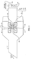
- FIG. 1 illustrates in a simplified schematic view (especially with regard to the pressure sensing chamber) an intra-ocular pressure sensor probe in which the probe has a cannula end portion 11 which is inserted into the eyeball, typically of a human being, for irrigation and/or fluid pressure sensing purposes and then a fluid input end 12 which, as indicated, is connected to a fluid supply hose which would carry various electrical leads. Intermediate the two ends 11 and 12 is an extended pair of shoulders 13 to provide a mechanical stop for the cannula end portion 11. Input end portion 12 receives fluid through the flow channel 16 which has a cross-section of approximately .5 millimeter. The entire structure is micro-miniature in size and would be, for example, less than 10 millimeters in length and having a width of approximately 1 millimeter.
- the flow channel 16 for the fluid is shown again at 16' where four pressure sensing piezoresistors are attached (actually embedded) to a silicon pressure sensing membrane (not directly shown) which is directly exposed to the fluid in the flow channel to measure its pressure.
- the four piezoresistors are representationally illustrated as opposed pairs R1 and R2 and opposed orthogonal pairs R3 and R4.
- the pressure sensing chamber is actually sealed and is shown open only for illustrative purposes. As will be described in detail below (see FIG.
- the piezoresistors are connected in a Wheatstone bridge format and as indicated there are four electrical leads including ground, supply voltage, V dd , and then a pair of voltages, V o1 and V o2 , the difference of which, V out , provides a measure of pressure.
- the pressure sensor Since the pressure sensor is in very close proximity to the interior of the eye, there is very little pressure drop in, for example, the 4 to 5 millimeter flow channel distance to the interior of the eye. Therefore, a very precise pressure measurement is made.
- the fluid supply system would utilize the voltage output of the pressure sensing probe to provide for automatic feedback control to maintain the pressure of the fluid in the eye to an exact desired amount.
- the cannula end portion 11 has a beveled tip 11' for easy insertion into the incision of the eye.
- the shoulders 13 and their transition to cannula 11 may either be right-angled or beveled as shown. As will be discussed below, very sharp angles are possible because of the deep plasma etching technique used in the fabrication of the device of FIG. 1.
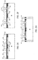
- FIGS. 2A-2G Such fabrication is illustrated in FIGS. 2A-2G.
- two separate silicon wafers 20 and 21 are used where in wafer 21 a plurality of flow channels are fabricated (depending on the size of the wafer several hundred although only four are indicated for purposes of illustration) and as shown by the cross-section 22 illustrated in FIG. 2C.
- the flow channel has a cannula end 11, a fluid input end 12 and an open top.
- the cross-section indicated as 22 is in effect shown in FIG. 1 where it is terminated by the dashed line 23.
- the flow channel is U-shaped with a bottom 24 and with legs 25a, 25b to thus provide an open top.
- FIG. 2B illustrates the other semiconductor wafer 20 where a plurality of pressure sensors are fabricated.
- a cross-section is illustrated in FIG. 2D across the section D-D indicated in FIG. 2B. Except as will be indicated below, this is a standard pressure sensor having a silicon base 26, a U-shaped cavity 27 with an n-type silicon layer 28 covering the cavity. The portion 29 of layer 28 overlying the cavity is in effect a silicon pressure sensing membrane. When the top 31 of this membrane 29 is exposed to the fluid in the channel 16, it will deform and the amount of deformation as indicated by the piezoelectric resistors. Two of them are partially shown as R1 and R2. They are, of course, an integral part of membrane 29 and layer 28. Then, in accordance with the invention a p++ layer is diffused in the "n" layer 28 in electrical contact with the piezoresistive elements R1 and R2. These layers indicated in a darker format are 33 and 34.
- FIG. 2E illustrates the opening of vias or contact openings which is accomplished with potassium hydroxide (KOH).
- KOH potassium hydroxide
- FIG. 2G by using a high density ionized gas through wafer etching is accomplished as indicated at 41 and 42 to release the individual bonded components.
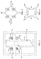
- FIG. 3 shows the process in greater detail where the actual mask pattern is shown at 51.
- the silicon pressure sensing membrane outline is illustrated at 29.
- the four electrical contacts discussed in FIG. 1 are shown by the dark portions and are appropriately labeled.
- the deep through wafer etching does not release the bonded components of each pressure sensing probe completely but rather a pair of tethers 52 and 53 still retain the sensing probe. Then at the appropriate time, the tethers are broken to remove the bonded silicon components or pairs for final connection to a hose with leads (FIG. 1).
- FIG. 4 illustrates the pressure sensing membrane 29 and its relationship to the four piezoresistive elements R1, R2, R3 and R4. Also, the electrical contacts relative to FIG. 3 are labeled.
- the pressure sensing membrane 29 forms a continuous planar portion of the flow channel 16 so that no fluid turbulence is caused.
- the entire structure is made of a monolithic semiconductive material, such as silicon, it is possible to fully integrate the pressure sensor with the flow channel and cannula to locate the pressure sensor very close to the end of the cannula which is inserted into the eye to minimize error causing pressure drop in the flow channel. Also, no turbulence is introduced. This is all made possible by the monolithic construction described above.
- both an improved intra-ocular pressure sensor miniature structure has been provided along with a novel fabrication method which includes, of course, the use of the p++ etch stop. This, again, provides easy electrical access to the piezoresistive elements.
Landscapes
- Life Sciences & Earth Sciences (AREA)
- Health & Medical Sciences (AREA)
- Medical Informatics (AREA)
- Biophysics (AREA)
- Ophthalmology & Optometry (AREA)
- Engineering & Computer Science (AREA)
- Biomedical Technology (AREA)
- Heart & Thoracic Surgery (AREA)
- Physics & Mathematics (AREA)
- Molecular Biology (AREA)
- Surgery (AREA)
- Animal Behavior & Ethology (AREA)
- General Health & Medical Sciences (AREA)
- Public Health (AREA)
- Veterinary Medicine (AREA)
- Measuring Fluid Pressure (AREA)
Description
- The present invention is directed to a monolithic silicon intra-ocular pressure sensor and a method of construction therefor and, more specifically, to a sensing probe having a cannula end portion for insertion into a human eye for irrigation or for sensing the intra-ocular pressure (IOP) fluid in the interior of the eye.
- During eye surgery, techniques to flush the cavities of the eye are hindered by the need to apply a tonometer and then manually adjust the flow to maintain proper pressure. Moreover, devices that continuously monitor intra-ocular pressure (IOP) often deliver erroneous values due to the sensor's distance from the eye. The mounting of a sensor closer to the eye entails mechanical problems due to the micro-miniature (that is several millimeters) size of the sensing probe and the fluid delivery system and the need to minimize surgical trauma.
- Document US4722350 shows an intraocular pressure sensing probe having a cannula end portion for insertion into an eye for irrigation and comprising a pressure sensing probe at the tip. Document US5591139 shows needles or cannulas in a monolithic silicon substrate with an integrated microdetector. Implantable eye pressure sensors are also known from DE 44 38 201 and US4922913.
- It is, therefore, an object of the present invention to provide a monolithic silicon intra-ocular pressure sensor and method therefor as defined in
claims 1, 4, 8. - In accordance with the above object, there is provided an intra-ocular pressure (IOP) sensing probe having a cannula end portion for insertion into an eye for irrigation or for sensing the IOP of fluid in the interior of the eye comprising a monolithic silicon sensor/cannula having a cannula portion, a flow channel portion for receiving fluid from an external source, and pressure sensing piezoresistors attached to a silicon pressure sensing membrane which is directly exposed to said fluid.
- From a method standpoint, there is provided a micro electromechanical (MEM) process of making an intra-ocular pressure (IOP) sensing probe having a cannula end portion for insertion into the eye for irrigation or for sensing IOP of fluid in the interior of the eye comprising the following steps. In a first semiconductor silicon wafer fabricating a plurality of flow channels with a cannula end and a fluid input end and having an open top. In a second semiconductor wafer fabricating a plurality of pressure sensors having wheatstone bridge-type piezoresistive elements adjacent to a pressure deformable silicon membrane in a mirror configuration of the flow channels. Aligning with and monolithically bonding said flow channels to said mating pressure sensors and releasing the bonded components by through wafer etching.
-
- FIG. 1 is a perspective view which is simplified of an intra-ocular pressure sensing probe incorporating the present invention;
- FIGS. 2A-2G are plan and cross-sectional views showing the construction of the device of the present invention;
- FIG. 3 is a plan view illustrating a step in the construction of the present invention;
- FIG. 4 is a simplified cross-sectional view of a portion of FIG. 3 illustrating piezoresistive elements; and
- FIG. 5 is a schematic circuit representation of FIG. 4.
-
- FIG. 1 illustrates in a simplified schematic view (especially with regard to the pressure sensing chamber) an intra-ocular pressure sensor probe in which the probe has a
cannula end portion 11 which is inserted into the eyeball, typically of a human being, for irrigation and/or fluid pressure sensing purposes and then a fluid input end 12 which, as indicated, is connected to a fluid supply hose which would carry various electrical leads. Intermediate the twoends 11 and 12 is an extended pair ofshoulders 13 to provide a mechanical stop for thecannula end portion 11. Input end portion 12 receives fluid through theflow channel 16 which has a cross-section of approximately .5 millimeter. The entire structure is micro-miniature in size and would be, for example, less than 10 millimeters in length and having a width of approximately 1 millimeter. - As illustrated in a representational manner only, the
flow channel 16 for the fluid is shown again at 16' where four pressure sensing piezoresistors are attached (actually embedded) to a silicon pressure sensing membrane (not directly shown) which is directly exposed to the fluid in the flow channel to measure its pressure. The four piezoresistors are representationally illustrated as opposed pairs R1 and R2 and opposed orthogonal pairs R3 and R4. The pressure sensing chamber is actually sealed and is shown open only for illustrative purposes. As will be described in detail below (see FIG. 5), the piezoresistors are connected in a Wheatstone bridge format and as indicated there are four electrical leads including ground, supply voltage, Vdd, and then a pair of voltages, Vo1 and Vo2, the difference of which, Vout, provides a measure of pressure. - Since the pressure sensor is in very close proximity to the interior of the eye, there is very little pressure drop in, for example, the 4 to 5 millimeter flow channel distance to the interior of the eye. Therefore, a very precise pressure measurement is made. In normal practice, the fluid supply system would utilize the voltage output of the pressure sensing probe to provide for automatic feedback control to maintain the pressure of the fluid in the eye to an exact desired amount.
- Finally, as illustrated in FIG. 1, the
cannula end portion 11 has a beveled tip 11' for easy insertion into the incision of the eye. Also, theshoulders 13 and their transition tocannula 11 may either be right-angled or beveled as shown. As will be discussed below, very sharp angles are possible because of the deep plasma etching technique used in the fabrication of the device of FIG. 1. - Such fabrication is illustrated in FIGS. 2A-2G. Initially as illustrated in FIGS. 2A and 2B, two
separate silicon wafers cross-section 22 illustrated in FIG. 2C. The flow channel has acannula end 11, a fluid input end 12 and an open top. The cross-section indicated as 22 is in effect shown in FIG. 1 where it is terminated by thedashed line 23. Specifically, the flow channel is U-shaped with abottom 24 and withlegs - FIG. 2B illustrates the
other semiconductor wafer 20 where a plurality of pressure sensors are fabricated. A cross-section is illustrated in FIG. 2D across the section D-D indicated in FIG. 2B. Except as will be indicated below, this is a standard pressure sensor having asilicon base 26, aU-shaped cavity 27 with an n-type silicon layer 28 covering the cavity. Theportion 29 oflayer 28 overlying the cavity is in effect a silicon pressure sensing membrane. When thetop 31 of thismembrane 29 is exposed to the fluid in thechannel 16, it will deform and the amount of deformation as indicated by the piezoelectric resistors. Two of them are partially shown as R1 and R2. They are, of course, an integral part ofmembrane 29 andlayer 28. Then, in accordance with the invention a p++ layer is diffused in the "n"layer 28 in electrical contact with the piezoresistive elements R1 and R2. These layers indicated in a darker format are 33 and 34. - In the next step as illustrated in FIG. 2E, the
wafer 21 of FIG. 2A is flipped and bonded to thewafer 20 of FIG. 2B. Thus, thesurface 31 of thesilicon membrane 28 is exposed to the fluid in the enclosedflow channel 16 which has been formed by the above process. Thesilicon base 26 is then thinned to the size shown. FIG. 2F illustrates the opening of vias or contact openings which is accomplished with potassium hydroxide (KOH). This etching in accordance with the present invention is stopped by thep++ areas silicon areas 28 are heavily doped near their solid solubility limit by a p-type material, they display a great resistance to etching in KOH. Thus, they serve as natural etch stops for the via formations. - After the etch procedure,
aluminum metallizing membrane 29 is different. Thus, the arrows shown in FIG. 5 indicate when the membrane is moved by ambient fluid pressure a positive resistance change occurs for R1 and R2 and a relative negative change for R3 and R4. This relative change is known in the art. - As shown in FIG. 2G, by using a high density ionized gas through wafer etching is accomplished as indicated at 41 and 42 to release the individual bonded components. FIG. 3 shows the process in greater detail where the actual mask pattern is shown at 51. The silicon pressure sensing membrane outline is illustrated at 29. And the four electrical contacts discussed in FIG. 1 are shown by the dark portions and are appropriately labeled. The deep through wafer etching, however, does not release the bonded components of each pressure sensing probe completely but rather a pair of
tethers - FIG. 4 illustrates the
pressure sensing membrane 29 and its relationship to the four piezoresistive elements R1, R2, R3 and R4. Also, the electrical contacts relative to FIG. 3 are labeled. - Referring to FIGS. 2E, 2F and 2G, it is apparent that the
pressure sensing membrane 29 forms a continuous planar portion of theflow channel 16 so that no fluid turbulence is caused. Then, as discussed above, since the entire structure is made of a monolithic semiconductive material, such as silicon, it is possible to fully integrate the pressure sensor with the flow channel and cannula to locate the pressure sensor very close to the end of the cannula which is inserted into the eye to minimize error causing pressure drop in the flow channel. Also, no turbulence is introduced. This is all made possible by the monolithic construction described above. Thus, both an improved intra-ocular pressure sensor miniature structure has been provided along with a novel fabrication method which includes, of course, the use of the p++ etch stop. This, again, provides easy electrical access to the piezoresistive elements.
Claims (9)
- An intra-ocular pressure (IOP) sensing probe having a cannula end portion for insertion into an eye for irrigation or for sensing the IOP of fluid in the interior of the eye comprising:
a monolithic silicon combined sensor and cannula having a said cannula portion (11), a flow channel portion (16) for receiving fluid from an external source, and pressure sensing piezoresistors (R1-R4) attached to a silicon pressure sensing membrane (29) which is directly exposed to said fluid. - An intra-ocular pressure sensing probe as in Claim 1 where said monolithic silicon sensor/cannula includes intermediate extending shoulder means to provide a mechanical stop for said cannula end portion.
- An IOP sensing probe as in Claim 1 where said sensing membrane forms a continuous planar portion of said flow channel whereby no fluid turbulence is caused.
- A micro electromechanical (MEM) process of making an intra-ocular pressure (IOP) sensing probe having a cannula end portion for insertion into the eye for irrigation or for sensing IOP of fluid in the interior of the eye comprising the following steps:in a first semiconductor silicon wafer fabricating a plurality of flow channels with a cannula end and a fluid input end and having an open top;in a second semiconductor wafer fabricating a plurality of pressure sensors having Wheatstone bridge-type piezoresistive elements adjacent to a pressure deformable silicon membrane in a mirror configuration of said flow channels;aligning with and monolithically bonding said flow channels to said mating pressure sensors; andreleasing said bonded components by through wafer etching.
- A process as in Claim 4 where in said through wafer etching step extended shoulder portions are formed to provide a mechanical stop for said cannula end.
- A process as in Claim 4 where in said step where said bonded components are released by said through wafer etching, said bonded components are still tethered and thereafter cutting said tethers to fully release said bonded components.
- A process as in Claim 4 including the step of heavily doping p++ areas of said pressure sensors adjacent said piezoresistive elements and then etching to said p++ areas which provide an etch stop and thereafter aluminizing said etched areas to provide electrical contacts for corners of said Wheatstone bridge.
- A micro electromechanical (MEM) process of making an intra-ocular pressure sensing (IOP) probe having a cannula end portion for insertion into the eye for irrigation or for sensing IOP of fluid in the interior of the eye comprising the following steps:1) in one silicon semiconductive wafer making a plurality of pressure sensors with four piezoresistive elements forming a Wheatstone bridge around a pressure deformable silicon membrane including the step of diffusing a p++ layer in electrical contact with said piezoresistive elements;2) in another silicon semiconductive wafer etching a plurality of mating flow channels including a cannula end portion and fluid input end;3) flipping said flow channels on said mating pressure sensors and bonding;4) thinning the silicon pressure sensor wafer;5) opening vias (contact openings) with potassium hydroxide which is stopped by said p++ areas and metallizing said open vias to form electrical contacts;6) providing a mask pattern for said bonded wafers which provides between said cannula and input ends extended shoulders which serve as a stop for said cannula end and deep silicon etching said bonded wafers leaving silicon tethers to retain the resultant etched bonded components;7) breaking said tethers to remove said bonded silicon components; and8) making electrically contacting wire connections to said metallized vias.
- A process as in Claim 4 where said through wafer etching is done by a high density ionized gas whereby sharp corners are provided.
Applications Claiming Priority (2)
| Application Number | Priority Date | Filing Date | Title |
|---|---|---|---|
| US09/145,150 US6010461A (en) | 1998-09-01 | 1998-09-01 | Monolithic silicon intra-ocular pressure sensor and method therefor |
| US145150 | 1998-09-01 |
Publications (2)
| Publication Number | Publication Date |
|---|---|
| EP0988826A1 EP0988826A1 (en) | 2000-03-29 |
| EP0988826B1 true EP0988826B1 (en) | 2002-01-09 |
Family
ID=22511812
Family Applications (1)
| Application Number | Title | Priority Date | Filing Date |
|---|---|---|---|
| EP99306690A Expired - Lifetime EP0988826B1 (en) | 1998-09-01 | 1999-08-23 | Monolithic silicon intra-ocular pressure sensor and manufacturing method therefor |
Country Status (4)
| Country | Link |
|---|---|
| US (1) | US6010461A (en) |
| EP (1) | EP0988826B1 (en) |
| CA (1) | CA2281301C (en) |
| DE (1) | DE69900771T2 (en) |
Cited By (1)
| Publication number | Priority date | Publication date | Assignee | Title |
|---|---|---|---|---|
| US9549851B2 (en) | 2015-01-28 | 2017-01-24 | Novartis Ag | Surgical hand piece with integrated pressure sensor |
Families Citing this family (25)
| Publication number | Priority date | Publication date | Assignee | Title |
|---|---|---|---|---|
| US6740058B2 (en) * | 2001-06-08 | 2004-05-25 | Wisconsin Alumni Research Foundation | Surgical tool with integrated pressure and flow sensors |
| US6685302B2 (en) | 2001-10-31 | 2004-02-03 | Hewlett-Packard Development Company, L.P. | Flextensional transducer and method of forming a flextensional transducer |
| US7770436B2 (en) * | 2001-10-31 | 2010-08-10 | Rheosense, Inc. | Micro rheometer for measuring flow viscosity and elasticity for micron sample volumes |
| US20050159660A1 (en) * | 2002-05-31 | 2005-07-21 | Valentino Montegrande | Intraocular pressure sensor |
| US20070123767A1 (en) * | 2002-05-31 | 2007-05-31 | Valentino Montegrande | Intraocular pressure sensor and method of use |
| US6883903B2 (en) * | 2003-01-21 | 2005-04-26 | Martha A. Truninger | Flextensional transducer and method of forming flextensional transducer |
| US20070276193A1 (en) * | 2003-11-27 | 2007-11-29 | Florence Rivera | Vivo Diagnostic and Therapy Micro-Device |
| US20050182312A1 (en) * | 2004-02-12 | 2005-08-18 | Medtronic Xomed, Inc. | Contact tonometer using MEMS technology |
| US20070170528A1 (en) | 2006-01-20 | 2007-07-26 | Aaron Partridge | Wafer encapsulated microelectromechanical structure and method of manufacturing same |
| WO2008151328A2 (en) * | 2007-06-08 | 2008-12-11 | Cornell University | Microprobes |
| FR2919486B1 (en) * | 2007-07-31 | 2009-10-02 | Captomed Entpr Unipersonnelle | SELF-CALIBRAL PRESSURE SENSOR. |
| WO2009073562A1 (en) * | 2007-12-03 | 2009-06-11 | Kolo Technologies, Inc. | Dual-mode operation micromachined ultrasonic transducer |
| EP2564181B1 (en) | 2010-04-26 | 2021-08-25 | RheoSense, Inc. | Portable viscometer |
| WO2012098160A1 (en) * | 2011-01-18 | 2012-07-26 | Imec | Disposable protection for micro-engineered devices |
| PL2766064T3 (en) | 2011-12-08 | 2017-08-31 | Alcon Research, Ltd. | Selectively moveable valve elements for aspiration and irrigation circuits |
| US9101444B2 (en) | 2012-01-12 | 2015-08-11 | Innfocus, Inc. | Method, surgical kit and device for treating glaucoma |
| US10016132B2 (en) | 2013-03-07 | 2018-07-10 | The Board Of Trustees Of The Leland Stanford Junior University | Implantable micro-fluidic device for monitoring of intra-ocular pressure |
| US10219696B2 (en) | 2013-03-07 | 2019-03-05 | The Board Of Trustees Of The Leland Stanford Junior University | Implantable pressure sensors for telemetric measurements through bodily tissues |
| US9549850B2 (en) | 2013-04-26 | 2017-01-24 | Novartis Ag | Partial venting system for occlusion surge mitigation |
| WO2015157698A1 (en) | 2014-04-11 | 2015-10-15 | Rheosense, Inc. | Viscometer and methods for using the same |
| EP3209237A4 (en) | 2014-10-24 | 2018-06-06 | Covidien LP | Sensorizing robotic surgical system access ports |
| US11291377B2 (en) | 2015-03-31 | 2022-04-05 | California Institute Of Technology | Biocompatible packaging for long term implantable sensors and electronics |
| CN110520031B (en) | 2017-05-12 | 2023-02-21 | 加州理工学院 | Implantable extra-luminal pressure sensor |
| US11701504B2 (en) | 2020-01-17 | 2023-07-18 | California Institute Of Technology | Implantable intracranial pressure sensor |
| EP4337285A4 (en) | 2021-05-10 | 2025-03-26 | RheoSense, Inc. | REDUCED DEAD VOLUME AND HIGH DYNAMIC RANGE VISCOMETER |
Family Cites Families (20)
| Publication number | Priority date | Publication date | Assignee | Title |
|---|---|---|---|---|
| US4023562A (en) * | 1975-09-02 | 1977-05-17 | Case Western Reserve University | Miniature pressure transducer for medical use and assembly method |
| US4166269A (en) * | 1978-03-06 | 1979-08-28 | Signetics Corporation | Temperature compensated piezoresistive transducer |
| US4722350A (en) * | 1984-09-21 | 1988-02-02 | Armeniades C D | Ophthalmic instrument for measuring intraocular fluid pressure |
| NL8502543A (en) * | 1985-09-17 | 1987-04-16 | Sentron V O F | ELECTRONIC PRESSURE SENSITIVE ELEMENT MADE OF SEMICONDUCTOR MATERIAL. |
| US4874500A (en) * | 1987-07-15 | 1989-10-17 | Sri International | Microelectrochemical sensor and sensor array |
| US4922913A (en) * | 1987-11-12 | 1990-05-08 | Waters Jr George E | Intraocular pressure sensor |
| US5062302A (en) * | 1988-04-29 | 1991-11-05 | Schlumberger Industries, Inc. | Laminated semiconductor sensor with overpressure protection |
| US4870964A (en) * | 1988-06-16 | 1989-10-03 | Paul F. Bailey, Jr. | Opthalmic surgical device and method with image data reflected off of the eye |
| US4993143A (en) * | 1989-03-06 | 1991-02-19 | Delco Electronics Corporation | Method of making a semiconductive structure useful as a pressure sensor |
| US5189777A (en) * | 1990-12-07 | 1993-03-02 | Wisconsin Alumni Research Foundation | Method of producing micromachined differential pressure transducers |
| EP0692266B1 (en) * | 1991-08-21 | 2000-03-22 | Smith & Nephew, Inc. | Fluid management system |
| DE4309207C2 (en) * | 1993-03-22 | 1996-07-11 | Texas Instruments Deutschland | Semiconductor device with a piezoresistive pressure sensor |
| US5668319A (en) * | 1994-02-07 | 1997-09-16 | The Regents Of The University Of California | Micromachined accelerometer |
| US5711302A (en) * | 1994-03-03 | 1998-01-27 | Merit Medical Systems, Inc. | Disposable transducer with digital processing and readout |
| US5591139A (en) * | 1994-06-06 | 1997-01-07 | The Regents Of The University Of California | IC-processed microneedles |
| JP3679143B2 (en) * | 1994-06-30 | 2005-08-03 | 株式会社ニデック | Perfusion suction device |
| EP0702221A3 (en) * | 1994-09-14 | 1997-05-21 | Delco Electronics Corp | One-chip integrated sensor |
| DE4438201C2 (en) * | 1994-10-26 | 1997-01-30 | Gerhard Heinrich Dr In Steeger | Device for long-term normalization of aqueous humor outflow from the human eye |
| US5701905A (en) * | 1995-11-13 | 1997-12-30 | Localmed, Inc. | Guide catheter with sensing element |
| US5879572A (en) * | 1996-11-19 | 1999-03-09 | Delco Electronics Corporation | Method of protecting silicon wafers during wet chemical etching |
-
1998
- 1998-09-01 US US09/145,150 patent/US6010461A/en not_active Expired - Fee Related
-
1999
- 1999-08-23 DE DE69900771T patent/DE69900771T2/en not_active Expired - Fee Related
- 1999-08-23 EP EP99306690A patent/EP0988826B1/en not_active Expired - Lifetime
- 1999-08-31 CA CA002281301A patent/CA2281301C/en not_active Expired - Fee Related
Cited By (1)
| Publication number | Priority date | Publication date | Assignee | Title |
|---|---|---|---|---|
| US9549851B2 (en) | 2015-01-28 | 2017-01-24 | Novartis Ag | Surgical hand piece with integrated pressure sensor |
Also Published As
| Publication number | Publication date |
|---|---|
| CA2281301C (en) | 2003-11-11 |
| US6010461A (en) | 2000-01-04 |
| EP0988826A1 (en) | 2000-03-29 |
| CA2281301A1 (en) | 2000-03-01 |
| DE69900771T2 (en) | 2002-08-14 |
| DE69900771D1 (en) | 2002-02-28 |
Similar Documents
| Publication | Publication Date | Title |
|---|---|---|
| CA2281301C (en) | Monolithic silicon intra-ocular pressure sensor and method therefor | |
| US8975671B2 (en) | Microelectromechanical semiconductor component that is sensitive to mechanical stresses, and comprises an ion implantation masking material defining a channel region | |
| US6263740B1 (en) | CMOS compatible integrated pressure sensor | |
| US4814856A (en) | Integral transducer structures employing high conductivity surface features | |
| Kalvesten et al. | The first surface micromachined pressure sensor for cardiovascular pressure measurements | |
| US4023562A (en) | Miniature pressure transducer for medical use and assembly method | |
| US5725729A (en) | Process for micromechanical fabrication | |
| CA2424529C (en) | System for measuring intraocular pressure of an eye and a mem sensor for use therewith | |
| US5295395A (en) | Diaphragm-based-sensors | |
| JPH09149941A (en) | Sensor for intra-corporeal medical instrument | |
| US20020151100A1 (en) | Pressure sensor monolithically integrated and relative process of fabrication | |
| EP0506491A2 (en) | An overpressure-protected differential pressure sensor and method of making the same | |
| EP1307720A1 (en) | Surface-micromachined pressure sensor and high pressure application | |
| US6619133B1 (en) | Semiconductor pressure sensor and its manufacturing method | |
| GB2276979A (en) | Capacitive surface micromachined absolute pressure sensor | |
| KR20000018637A (en) | Seal-like, wireless element for measuring pressure and a process for production thereof | |
| JPH09501231A (en) | Electrostatic force balance type silicon accelerometer | |
| US5672551A (en) | Method for manufacturing a semiconductor pressure sensor with single-crystal silicon diaphragm and single-crystal gage elements | |
| US5172205A (en) | Piezoresistive semiconductor device suitable for use in a pressure sensor | |
| EP2166330A1 (en) | Miniature pressure transducer with elongate base wafer and operable at high temperatures | |
| CN115985851A (en) | Pressure sensor and manufacturing method thereof | |
| JPH04299871A (en) | Semiconductor pressure sensor and its manufacture | |
| CN113227740B (en) | Micromechanical pressure sensor device and corresponding manufacturing method | |
| Gowrishetty et al. | Development of ultra-miniature pressure sensors for 1-French biomedical applications and beyond | |
| US20050029607A1 (en) | Device for capacitive pressure measurement and method for manufacturing a capacitive pressure measuring device |
Legal Events
| Date | Code | Title | Description |
|---|---|---|---|
| PUAI | Public reference made under article 153(3) epc to a published international application that has entered the european phase |
Free format text: ORIGINAL CODE: 0009012 |
|
| 17P | Request for examination filed |
Effective date: 19990903 |
|
| AK | Designated contracting states |
Kind code of ref document: A1 Designated state(s): DE FR GB |
|
| AX | Request for extension of the european patent |
Free format text: AL;LT;LV;MK;RO;SI |
|
| AKX | Designation fees paid |
Free format text: AT BE CH LI |
|
| RIN1 | Information on inventor provided before grant (corrected) |
Inventor name: MONTEGRANDE, KEVIN Inventor name: HUANG, YONGLI Inventor name: LIM, MARTIN Inventor name: HANIFF, TARIQ M. |
|
| RBV | Designated contracting states (corrected) |
Designated state(s): DE FR GB |
|
| GRAG | Despatch of communication of intention to grant |
Free format text: ORIGINAL CODE: EPIDOS AGRA |
|
| 17Q | First examination report despatched |
Effective date: 20010828 |
|
| GRAG | Despatch of communication of intention to grant |
Free format text: ORIGINAL CODE: EPIDOS AGRA |
|
| GRAH | Despatch of communication of intention to grant a patent |
Free format text: ORIGINAL CODE: EPIDOS IGRA |
|
| GRAH | Despatch of communication of intention to grant a patent |
Free format text: ORIGINAL CODE: EPIDOS IGRA |
|
| GRAA | (expected) grant |
Free format text: ORIGINAL CODE: 0009210 |
|
| REG | Reference to a national code |
Ref country code: GB Ref legal event code: IF02 |
|
| AK | Designated contracting states |
Kind code of ref document: B1 Designated state(s): DE FR GB |
|
| REF | Corresponds to: |
Ref document number: 69900771 Country of ref document: DE Date of ref document: 20020228 |
|
| ET | Fr: translation filed | ||
| PLBE | No opposition filed within time limit |
Free format text: ORIGINAL CODE: 0009261 |
|
| STAA | Information on the status of an ep patent application or granted ep patent |
Free format text: STATUS: NO OPPOSITION FILED WITHIN TIME LIMIT |
|
| 26N | No opposition filed | ||
| PGFP | Annual fee paid to national office [announced via postgrant information from national office to epo] |
Ref country code: GB Payment date: 20030827 Year of fee payment: 5 Ref country code: FR Payment date: 20030827 Year of fee payment: 5 |
|
| PGFP | Annual fee paid to national office [announced via postgrant information from national office to epo] |
Ref country code: DE Payment date: 20030904 Year of fee payment: 5 |
|
| PG25 | Lapsed in a contracting state [announced via postgrant information from national office to epo] |
Ref country code: GB Free format text: LAPSE BECAUSE OF NON-PAYMENT OF DUE FEES Effective date: 20040823 |
|
| PG25 | Lapsed in a contracting state [announced via postgrant information from national office to epo] |
Ref country code: DE Free format text: LAPSE BECAUSE OF NON-PAYMENT OF DUE FEES Effective date: 20050301 |
|
| GBPC | Gb: european patent ceased through non-payment of renewal fee |
Effective date: 20040823 |
|
| PG25 | Lapsed in a contracting state [announced via postgrant information from national office to epo] |
Ref country code: FR Free format text: LAPSE BECAUSE OF NON-PAYMENT OF DUE FEES Effective date: 20050429 |
|
| REG | Reference to a national code |
Ref country code: FR Ref legal event code: ST |