EP0986149A2 - Optical amplifier - Google Patents
Optical amplifier Download PDFInfo
- Publication number
- EP0986149A2 EP0986149A2 EP99307081A EP99307081A EP0986149A2 EP 0986149 A2 EP0986149 A2 EP 0986149A2 EP 99307081 A EP99307081 A EP 99307081A EP 99307081 A EP99307081 A EP 99307081A EP 0986149 A2 EP0986149 A2 EP 0986149A2
- Authority
- EP
- European Patent Office
- Prior art keywords
- output
- light
- variable gain
- current
- optical
- Prior art date
- Legal status (The legal status is an assumption and is not a legal conclusion. Google has not performed a legal analysis and makes no representation as to the accuracy of the status listed.)
- Granted
Links
Images


Classifications
-
- H—ELECTRICITY
- H01—ELECTRIC ELEMENTS
- H01S—DEVICES USING THE PROCESS OF LIGHT AMPLIFICATION BY STIMULATED EMISSION OF RADIATION [LASER] TO AMPLIFY OR GENERATE LIGHT; DEVICES USING STIMULATED EMISSION OF ELECTROMAGNETIC RADIATION IN WAVE RANGES OTHER THAN OPTICAL
- H01S3/00—Lasers, i.e. devices using stimulated emission of electromagnetic radiation in the infrared, visible or ultraviolet wave range
- H01S3/10—Controlling the intensity, frequency, phase, polarisation or direction of the emitted radiation, e.g. switching, gating, modulating or demodulating
- H01S3/13—Stabilisation of laser output parameters, e.g. frequency or amplitude
- H01S3/1301—Stabilisation of laser output parameters, e.g. frequency or amplitude in optical amplifiers
- H01S3/13013—Stabilisation of laser output parameters, e.g. frequency or amplitude in optical amplifiers by controlling the optical pumping
-
- H—ELECTRICITY
- H01—ELECTRIC ELEMENTS
- H01S—DEVICES USING THE PROCESS OF LIGHT AMPLIFICATION BY STIMULATED EMISSION OF RADIATION [LASER] TO AMPLIFY OR GENERATE LIGHT; DEVICES USING STIMULATED EMISSION OF ELECTROMAGNETIC RADIATION IN WAVE RANGES OTHER THAN OPTICAL
- H01S2301/00—Functional characteristics
- H01S2301/06—Gain non-linearity, distortion; Compensation thereof
-
- H—ELECTRICITY
- H01—ELECTRIC ELEMENTS
- H01S—DEVICES USING THE PROCESS OF LIGHT AMPLIFICATION BY STIMULATED EMISSION OF RADIATION [LASER] TO AMPLIFY OR GENERATE LIGHT; DEVICES USING STIMULATED EMISSION OF ELECTROMAGNETIC RADIATION IN WAVE RANGES OTHER THAN OPTICAL
- H01S3/00—Lasers, i.e. devices using stimulated emission of electromagnetic radiation in the infrared, visible or ultraviolet wave range
- H01S3/005—Optical devices external to the laser cavity, specially adapted for lasers, e.g. for homogenisation of the beam or for manipulating laser pulses, e.g. pulse shaping
- H01S3/0078—Frequency filtering
-
- H—ELECTRICITY
- H01—ELECTRIC ELEMENTS
- H01S—DEVICES USING THE PROCESS OF LIGHT AMPLIFICATION BY STIMULATED EMISSION OF RADIATION [LASER] TO AMPLIFY OR GENERATE LIGHT; DEVICES USING STIMULATED EMISSION OF ELECTROMAGNETIC RADIATION IN WAVE RANGES OTHER THAN OPTICAL
- H01S3/00—Lasers, i.e. devices using stimulated emission of electromagnetic radiation in the infrared, visible or ultraviolet wave range
- H01S3/05—Construction or shape of optical resonators; Accommodation of active medium therein; Shape of active medium
- H01S3/06—Construction or shape of active medium
- H01S3/063—Waveguide lasers, i.e. whereby the dimensions of the waveguide are of the order of the light wavelength
- H01S3/067—Fibre lasers
- H01S3/06754—Fibre amplifiers
-
- H—ELECTRICITY
- H01—ELECTRIC ELEMENTS
- H01S—DEVICES USING THE PROCESS OF LIGHT AMPLIFICATION BY STIMULATED EMISSION OF RADIATION [LASER] TO AMPLIFY OR GENERATE LIGHT; DEVICES USING STIMULATED EMISSION OF ELECTROMAGNETIC RADIATION IN WAVE RANGES OTHER THAN OPTICAL
- H01S3/00—Lasers, i.e. devices using stimulated emission of electromagnetic radiation in the infrared, visible or ultraviolet wave range
- H01S3/10—Controlling the intensity, frequency, phase, polarisation or direction of the emitted radiation, e.g. switching, gating, modulating or demodulating
- H01S3/13—Stabilisation of laser output parameters, e.g. frequency or amplitude
- H01S3/1305—Feedback control systems
Definitions
- the present invention relates to an optical amplifier, especially to an optical amplifier that is used in a multistage relay for a wavelength division multiplexing transmission system.
- Wavelength division multiplexing transmission which is a technology of high capacity communication, is now starting to be put to practical use.
- WDM transmission since any gain difference in each wavelength constituting a transmission wave becomes a big issue when a multistage relay is constructed with the optical amplifier, a low gain tilt is required.
- a wavelength synthesizing coupler 1 synthesizes excited light generated by an excited light source 6 and an input optical signal.
- a rare-earth element doped fiber 2 that has received the synthesized light optically amplifies the input signal by means of excited light in the synthesized light, and an isolator 3 prevents oscillation associated with the optical amplification.
- One output from an optical branch 4 that has received an output from the isolator 3 is converted into a current by a light receiving element 9, and an automatic gain control circuit 8 controls the output level of the excited light source 6 so as to make the output from an apparatus constant based on this current information.
- Other outputs from the optical branch 4 are input to an fixed gain equalizer 18 where the gain difference of each wavelength is equalized and which provide the output.
- JP-A-223136/1996 does not provide an effect by applying it to the individual relays, and also, since the method in JP-A-43647/1997 is for realizing gain equalization by mechanically bending a fiber, changes due to temperature characteristic and reliability are a matter of concern.
- a rare-earth element doped fiber amplifies input light by means of excited light issued by an excited light source.
- a part of the amplified light divided by a branch is converted into a current at a light receiving element, and an automatic gain control circuit controls the excited light source.
- An excited light receiving element receives excited light and converts it into a current, and based on the current information, a variable gain equalizer control circuit controls a variable gain equalizer and outputs amplified light having characteristic that the gain difference between different wavelengths is reduced.
- variable gain equalizer may be either at the output or at the input of the optical amplifier, and there may be more than one variable gain equalizer. In the latter case, one or more equalizers may be at the input and one or more at the output.
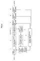
- Fig. 1 is an arrangement view of a first embodiment of an optical amplifier of the present invention.
- variable gain equalizer 5 is used instead of the fixed gain equalizer 16 of the optical amplifier of Fig. 8, and an excited light receiving element 7 and a variable gain equalizer control circuit 10 are added.
- the variable gain equalizer 5 is controlled by a control current having a radio frequency, and an acoustic wave optical element is used, in which a loss peak wavelength of light is changed by a frequency of the control current, and a quantity of light is changed by an amplitude of the control current (Publication: Single-mode-fiber acousto-optic tunable notch filter with variable spectral profile" Hyo Sang Kim, et al.: 1997, Proceedings of Conference on Optical Fiber Communication).
- the excited light receiving element 7 converts excited light generated by the excited light source 6 into a current.
- the variable gain equalizer control circuit 10 receives the current generated by the excited light receiving element 7, and based on the current information, generates a control current having a radio frequency, and controls the variable gain equalizer 5 based on information of a frequency and an amplitude which the generated control current has, and reduces a gain difference between the respective wavelengths of light amplified by a rare-earth element doped fiber 2, and outputs it.
- Fig. 2 shows one embodiment of the variable gain equalizer control circuit 10 of Fig. 1.
- variable gain equalizer control circuit 10 is consisted of a current/voltage conversion circuit 11, a Voltage Controlled Oscillator (referred to as VCO, hereinafter) 12, an amplifier 13, an amplification control circuit 14, and a drive circuit 16.
- VCO Voltage Controlled Oscillator
- the current/voltage conversion circuit 11 converts a value of a current generated by the excited light receiving element 7 into a voltage, and outputs it.
- the VCO 12 generates an alternating current having a radio frequency proportional to a voltage level generated by the current/voltage conversion circuit 11.
- the amplifier 13 amplifies the alternating current generated by the VCO 12.
- the amplification control circuit 14 controls a quantity of amplification of the amplifier 13 so as to comply with an input range of the drive circuit 16.
- the drive circuit 16 drives the variable gain equalizer 5 using a radio frequency current output by the amplifier 13 as a control current.
- An optical input signal input to the optical amplifier is optically amplified by the rare-earth element doped fiber 2 that is being excited by the excited light source 6.
- an optical output is divided at the optical branch 4, and in order to keep an optical output level constant by means of current information output from the light receiving element 9, an output level of the excited light source 6 is controlled by the automatic gain control circuit 8.
- an isolator 3 acts for preventing oscillation in the rare-earth element doped fiber 2.
- This optical amplifier has characteristic that a gain has dependence on a wavelength in an optical amplifier section 17 in which a variable gain equalizer is not included, as shown by broken lines a 1 , a 2 and a 3 of Fig.
- the optical amplifier shows condition of the broken line 1 ⁇ , and in accordance with enhancement of the level of the excited light, a wavelength at which a gain has a peak moves to a short wavelength in order of 2 ⁇ ⁇ 3 ⁇ .
- the automatic gain control circuit 8 acts so as to keep the output level of the light constant, and an excited light level of the excited light source 6 increases, and thereby, light that is input to the excited light receiving element 7 for converting an output level of the excited light source 6 into a current becomes to be large, and since a larger current occurs, a large voltage is generated by the current/voltage conversion circuit 11, and it is sensed that the excited light level has become to be large.
- variable gain equalizer 5 Since the variable gain equalizer 5 has characteristic that a wavelength at which a loss peak of light appears changes in accordance with a frequency of a control current and a quantity of loss of the light also changes in accordance with an amplitude of the control current, as shown by solid lines b 1 , b 2 and b 3 in a graph of Fig.
- the loss of a gain of the variable gain equalizer 5 is large as a level of the excited light becomes to be large, and by defining a frequency of a current generated by the VCO 12 so as to move a peak of the loss toward a short wavelength side, and controlling the amplifier 13 for amplifying an amplitude of the current by the amplification control circuit 14, output characteristic in which a gain difference between the respective wavelengths is obtained at an output terminal of the optical amplifier like solid lines c 1 , c 2 and c 3 shown on a right-hand side of Fig. 3.
- Fig. 4 is an arrangement view of a second embodiment of the optical amplifier of the present invention.
- variable gain equalizers 51 and 52 are inserted in series in the back of the variable gain equalizer 5 of the optical amplifier of Fig. 1, and the variable gain equalizers 51 and 52 are subject to the control by the variable gain equalizer control circuit 10, respectively, and further reduces a gain difference between the respective wavelengths of an input and amplified light and outputs it.
- variable gain equalizers In the optical amplifier of the second embodiment, although the three-stage variable gain equalizers are inserted in series, generally n variable gain equalizers can be used in series.
- Fig. 5 is an arrangement view of a third embodiment of the optical amplifier of the present invention.
- This optical amplifier has an arrangement same as that of the optical amplifier of Fig. 1, except that a variable gain equalizer 15 inserted in the front of a wavelength synthesizing coupler instead of the variable gain equalizer 5 of Fig. 1. Since the variable gain equalizer 15 is subject to the control by the variable gain equalizer control circuit 10 and functions so as to reduce a gain difference between the respective wavelengths of input light, the optical amplifier outputs amplified light in which the gain difference between the respective wavelengths is reduced.
- Fig. 6 is an arrangement view of a fourth embodiment of the optical amplifier of the present invention.
- variable gain equalizers 151 and 152 are inserted in series in the front of the variable gain equalizer 15 of the optical amplifier of Fig. 5, and since the variable gain equalizers 151 and 152 are subject to the control by the variable gain equalizer control circuit 10 and functions so as to further reduce a gain difference between the respective wavelengths of input light, output light from the optical amplifier has characteristic that the gain difference between the respective wavelengths is further reduced.
- variable gain equalizers are inserted in series, generally n variable gain equalizers can be used in series.
- Fig. 7 is an arrangement view of a fifth embodiment of the optical amplifier of the present invention.
- variable gain equalizer 15 same as that in Fig. 5 is inserted in the front of the wavelength synthesizing coupler 1 of Fig. 1, and the variable gain equalizer 15, together with the variable gain equalizer 5, is controlled by the variable gain equalizer control circuit 10.
- variable gain equalizers are adopted on an input side and an output side of the optical amplifier, and reduction of the gain difference between the respective wavelengths is effectively realized.
- variable gain equalizer In the optical amplifier of this embodiment, although one variable gain equalizer is used on each of the input side and the output side, it is possible to adopt an arrangement in which n variable gain equalizers are arranged, respectively, on the input side and the output side of the optical amplifier like in the second and third embodiments.
- variable gain equalizers and variable gain equalizer control means for controlling the variable gain equalizers in the present invention, it is possible to obtain output light having characteristic in which, even though a level of input light changes, a gain difference between respective wavelengths is reduced, the present invention effects an advantage that the optical amplifier applicable to a multistage relay of a WDM transmission system.
Landscapes
- Physics & Mathematics (AREA)
- Electromagnetism (AREA)
- Engineering & Computer Science (AREA)
- Plasma & Fusion (AREA)
- Optics & Photonics (AREA)
- Lasers (AREA)
- Optical Communication System (AREA)
Abstract
Description
- The present invention relates to an optical amplifier, especially to an optical amplifier that is used in a multistage relay for a wavelength division multiplexing transmission system.
- Wavelength division multiplexing transmission (WDM transmission), which is a technology of high capacity communication, is now starting to be put to practical use. However, in this WDM transmission system, since any gain difference in each wavelength constituting a transmission wave becomes a big issue when a multistage relay is constructed with the optical amplifier, a low gain tilt is required.
- In known gain equalization methods, either an optimum design has been calculated for each transmission system, or, like an optical amplifier used as an optical relay shown in Fig. 8, a fixed gain equalizer has been used.
- In the optical relay of Fig. 8, a
wavelength synthesizing coupler 1 synthesizes excited light generated by anexcited light source 6 and an input optical signal. A rare-earth element dopedfiber 2 that has received the synthesized light optically amplifies the input signal by means of excited light in the synthesized light, and anisolator 3 prevents oscillation associated with the optical amplification. One output from anoptical branch 4 that has received an output from theisolator 3 is converted into a current by alight receiving element 9, and an automaticgain control circuit 8 controls the output level of theexcited light source 6 so as to make the output from an apparatus constant based on this current information. Other outputs from theoptical branch 4 are input to anfixed gain equalizer 18 where the gain difference of each wavelength is equalized and which provide the output. - Also, as a method of obtaining optimum gain equalization in the transmission system, there is a disclosure JP-A-223136/1996, "Gain Equalization Method in Optical Amplification Relay Technique" by Mr. Fukutoku, et al., and as a method of improving a gain difference by wavelengths of an optical amplifier, there is a disclosure JP-A-43647/1997, "Gain Equalizer and Optical Amplifier" by Mr. Domon.
- With regard to the above-mentioned gain equalization method, in the method in which the optimum design for every transmission system is calculated, a difference between the design and actual fact is a matter of concern, and the method is not general. Also, in the method in which the fixed gain equalizer is used, there is a defect that a gain difference in each wavelength occurs by means of dependence on wavelength of the gain of the optical amplifier due to temperature or by means of dependence on wavelength of the gain of the optical amplifier based on the change of the input level, due to lack and so forth of an input signal during wavelength division multiplexing transmission. Furthermore, the method in JP-A-223136/1996 does not provide an effect by applying it to the individual relays, and also, since the method in JP-A-43647/1997 is for realizing gain equalization by mechanically bending a fiber, changes due to temperature characteristic and reliability are a matter of concern.
- The invention in its various aspects is defined in the independent claims below to which reference should now be made. Advantageous features are set forth in the appendant claims.
- A preferred embodiment of the invention is described in more detail below with reference to the drawings. In this preferred embodiment, a rare-earth element doped fiber amplifies input light by means of excited light issued by an excited light source. A part of the amplified light divided by a branch is converted into a current at a light receiving element, and an automatic gain control circuit controls the excited light source. An excited light receiving element receives excited light and converts it into a current, and based on the current information, a variable gain equalizer control circuit controls a variable gain equalizer and outputs amplified light having characteristic that the gain difference between different wavelengths is reduced.
- The variable gain equalizer may be either at the output or at the input of the optical amplifier, and there may be more than one variable gain equalizer. In the latter case, one or more equalizers may be at the input and one or more at the output.
- The present invention will now be described in detail by way of example with reference to the drawings, in which:
- Fig. 1 is an arrangement view of a first embodiment of an optical amplifier of the present invention,
- Fig. 2 is one embodiment of the variable gain
equalizer control circuit 10 of Fig. 1, - Fig. 3 is a view for explaining operation of the optical amplifier of Fig. 2,
- Fig. 4 is an arrangement view of a second embodiment of the optical amplifier of the present invention,
- Fig. 5 is an arrangement view of a third embodiment of the optical amplifier of the present invention,
- Fig. 6 is an arrangement view of a fourth embodiment of the optical amplifier of the present invention,
- Fig. 7 is an arrangement view of a fifth embodiment of the optical amplifier of the present invention and
- Fig. 8 is an arrangement view of a conventional example of an optical amplifier.
-
- Next, embodiments of the present invention will be explained by referring to drawings.
- Fig. 1 is an arrangement view of a first embodiment of an optical amplifier of the present invention.
- In this optical amplifier, a
variable gain equalizer 5 is used instead of thefixed gain equalizer 16 of the optical amplifier of Fig. 8, and an excitedlight receiving element 7 and a variable gainequalizer control circuit 10 are added. Thevariable gain equalizer 5 is controlled by a control current having a radio frequency, and an acoustic wave optical element is used, in which a loss peak wavelength of light is changed by a frequency of the control current, and a quantity of light is changed by an amplitude of the control current (Publication: Single-mode-fiber acousto-optic tunable notch filter with variable spectral profile" Hyo Sang Kim, et al.: 1997, Proceedings of Conference on Optical Fiber Communication). The excitedlight receiving element 7 converts excited light generated by theexcited light source 6 into a current. The variable gainequalizer control circuit 10 receives the current generated by the excitedlight receiving element 7, and based on the current information, generates a control current having a radio frequency, and controls thevariable gain equalizer 5 based on information of a frequency and an amplitude which the generated control current has, and reduces a gain difference between the respective wavelengths of light amplified by a rare-earth element dopedfiber 2, and outputs it. - Fig. 2 shows one embodiment of the variable gain
equalizer control circuit 10 of Fig. 1. - In this optical amplifier, the variable gain
equalizer control circuit 10 is consisted of a current/voltage conversion circuit 11, a Voltage Controlled Oscillator (referred to as VCO, hereinafter) 12, anamplifier 13, anamplification control circuit 14, and adrive circuit 16. - The current/
voltage conversion circuit 11 converts a value of a current generated by the excitedlight receiving element 7 into a voltage, and outputs it. TheVCO 12 generates an alternating current having a radio frequency proportional to a voltage level generated by the current/voltage conversion circuit 11. Theamplifier 13 amplifies the alternating current generated by theVCO 12. Theamplification control circuit 14 controls a quantity of amplification of theamplifier 13 so as to comply with an input range of thedrive circuit 16. Thedrive circuit 16 drives thevariable gain equalizer 5 using a radio frequency current output by theamplifier 13 as a control current. - Next, operation of this optical amplifier will be explained by referring to Fig. 2 and Fig. 3.
- An optical input signal input to the optical amplifier is optically amplified by the rare-earth element doped
fiber 2 that is being excited by theexcited light source 6. At this time, an optical output is divided at theoptical branch 4, and in order to keep an optical output level constant by means of current information output from thelight receiving element 9, an output level of theexcited light source 6 is controlled by the automaticgain control circuit 8. Here, anisolator 3 acts for preventing oscillation in the rare-earth element dopedfiber 2. This optical amplifier has characteristic that a gain has dependence on a wavelength in anoptical amplifier section 17 in which a variable gain equalizer is not included, as shown by broken lines a1, a2 and a3 of Fig. 3 1 ○ to 3 ○ for levels (Pumping power) of excited light generated by theexcited light source 6. In this case, if a level of the excited light is small, the optical amplifier shows condition of thebroken line 1 ○, and in accordance with enhancement of the level of the excited light, a wavelength at which a gain has a peak moves to a short wavelength in order of 2 ○ → 3 ○. For example, in case that an input level of the optical amplifier lowers, the automaticgain control circuit 8 acts so as to keep the output level of the light constant, and an excited light level of theexcited light source 6 increases, and thereby, light that is input to the excitedlight receiving element 7 for converting an output level of theexcited light source 6 into a current becomes to be large, and since a larger current occurs, a large voltage is generated by the current/voltage conversion circuit 11, and it is sensed that the excited light level has become to be large. - Since the
variable gain equalizer 5 has characteristic that a wavelength at which a loss peak of light appears changes in accordance with a frequency of a control current and a quantity of loss of the light also changes in accordance with an amplitude of the control current, as shown by solid lines b1, b2 and b3 in a graph of Fig. 3, the loss of a gain of thevariable gain equalizer 5 is large as a level of the excited light becomes to be large, and by defining a frequency of a current generated by theVCO 12 so as to move a peak of the loss toward a short wavelength side, and controlling theamplifier 13 for amplifying an amplitude of the current by theamplification control circuit 14, output characteristic in which a gain difference between the respective wavelengths is obtained at an output terminal of the optical amplifier like solid lines c1, c2 and c3 shown on a right-hand side of Fig. 3. - Fig. 4 is an arrangement view of a second embodiment of the optical amplifier of the present invention.
- In this optical amplifier,
variable gain equalizers variable gain equalizer 5 of the optical amplifier of Fig. 1, and thevariable gain equalizers equalizer control circuit 10, respectively, and further reduces a gain difference between the respective wavelengths of an input and amplified light and outputs it. - In the optical amplifier of the second embodiment, although the three-stage variable gain equalizers are inserted in series, generally n variable gain equalizers can be used in series.
- Fig. 5 is an arrangement view of a third embodiment of the optical amplifier of the present invention.
- This optical amplifier has an arrangement same as that of the optical amplifier of Fig. 1, except that a
variable gain equalizer 15 inserted in the front of a wavelength synthesizing coupler instead of thevariable gain equalizer 5 of Fig. 1. Since thevariable gain equalizer 15 is subject to the control by the variable gainequalizer control circuit 10 and functions so as to reduce a gain difference between the respective wavelengths of input light, the optical amplifier outputs amplified light in which the gain difference between the respective wavelengths is reduced. - Fig. 6 is an arrangement view of a fourth embodiment of the optical amplifier of the present invention.
- In this optical amplifier,
variable gain equalizers variable gain equalizer 15 of the optical amplifier of Fig. 5, and since thevariable gain equalizers equalizer control circuit 10 and functions so as to further reduce a gain difference between the respective wavelengths of input light, output light from the optical amplifier has characteristic that the gain difference between the respective wavelengths is further reduced. - In the optical amplifier of the fourth embodiment, although the three-stage variable gain equalizers are inserted in series, generally n variable gain equalizers can be used in series.
- Fig. 7 is an arrangement view of a fifth embodiment of the optical amplifier of the present invention.
- In this optical amplifier, a
variable gain equalizer 15 same as that in Fig. 5 is inserted in the front of thewavelength synthesizing coupler 1 of Fig. 1, and thevariable gain equalizer 15, together with thevariable gain equalizer 5, is controlled by the variable gainequalizer control circuit 10. - In this embodiment, the variable gain equalizers are adopted on an input side and an output side of the optical amplifier, and reduction of the gain difference between the respective wavelengths is effectively realized.
- In the optical amplifier of this embodiment, although one variable gain equalizer is used on each of the input side and the output side, it is possible to adopt an arrangement in which n variable gain equalizers are arranged, respectively, on the input side and the output side of the optical amplifier like in the second and third embodiments.
- As explained above, since, by providing one or more than one variable gain equalizers and variable gain equalizer control means for controlling the variable gain equalizers in the present invention, it is possible to obtain output light having characteristic in which, even though a level of input light changes, a gain difference between respective wavelengths is reduced, the present invention effects an advantage that the optical amplifier applicable to a multistage relay of a WDM transmission system.
Claims (9)
- An optical amplifier comprising:characterized by:an excited light source (6) for generating excited light;a wavelength synthesizing coupler (1) for synthesizing an input optical signal and excited light generated by said excited light source and outputting it;a rare-earth doped fiber (2) for receiving an output from said wavelength synthesizing coupler, and amplifying an input optical signal in said output, which is excited by excited light in said output;an optical branch (4) for receiving said amplified input optical signal which is output from said fiber, and dividing it into outputs and outputting them;a first light receiving element (9) for receiving a first output light from said optical branch, and converting it into a current;an automatic gain control circuit (8) for controlling an output level of said excited light source so as to make a level of a second output light from said optical branch constant, based on current information output from the first light receiving element;a second light receiving element (7) for receiving excited light output from said excited light source, and converting it into a current;one or more than one variable gain equalizers (5) for equalizing a gain difference of each wavelength of input light, and outputting it; andvariable gain equalization control means (10) for controlling said variable gain equalizers based on current information output from the second light receiving element so that a gain difference in each wavelength of light which is output from said variable gain equalizers becomes to be constant.
- An optical amplifier according to claim 1, wherein said variable gain equalization control means comprises:a current/voltage conversion circuit (11) for receiving a current generated by said second light receiving element, and converting it into a voltage;a voltage control frequency generator (12) for generating an alternating current having a frequency proportional to a level of a voltage generated by said current/voltage conversion circuit;an amplifier (13) for amplifying an amplitude of the alternating current generated by said voltage control frequency generator;a control circuit (14) for controlling said amplifier so that an amplitude of the alternating current output by said amplifier becomes to be a required value; anda drive circuit (16) for receiving an alternating current output by said amplifier, and driving said variable gain equalizers.
- An optical amplifier according to claim 1 or 2, wherein said wavelength synthesizing coupler (1), said rare-earth doped fiber (2), and said optical branch (4) form a series circuit, and wherein said variable gain equalizer (5; 15) is in series with said series circuit.
- An optical amplifier according to claim 1, 2 or 3, wherein said one or more than one variable gain equalizers (5; 5,51,52) are inserted after said optical branch (4).
- An optical amplifier according to claim 1, 2 or 3, wherein said one or more than one variable gain equalizers (15; 15,151,152) are inserted before said wavelength synthesizing coupler (1).
- An optical amplifier according to claim 1, 2 or 3, wherein variable gain equalizers (5,15) are inserted one or more after said optical branch (4) and one or more before said wavelength synthesizing coupler (1).
- An optical amplifier according to any of claims 1 to 6, wherein said one or more than one variable gain equalizers (5; 15) are controlled by said variable gain equalization control means.
- An optical amplifier according to any of claims 1 to 7, further comprising an isolator (3) connected to said rare-earth doped fiber (2) for preventing oscillation associated with optical amplification of said fiber.
- An optical amplifier comprising:characterized by:an excited light source (6) for generating excited light;a wavelength synthesizing coupler (1) for synthesizing an input optical signal and excited light generated by said excited light source and outputting it;a rare-earth doped fiber (2) for receiving an output from said wavelength synthesizing coupler, and amplifying an input optical signal in said output, which is excited by excited light in said output;an isolator (3) connected to said rare-earth doped fiber, for preventing oscillation associated with optical amplification of said fiber;an optical branch (4) for receiving said amplified input optical signal which is output from said isolator, and dividing it into outputs and outputting them;a first light receiving element (9) for receiving a first output light from said optical branch, and converting it into a current;an automatic gain control circuit (8) for controlling an output level of said excited light source so as to make a level of a second output light from said optical branch constant, based on current information output from the first light receiving element;a second light receiving element (7) for receiving excited light output from said excited light source, and converting it into a current;one or more than one variable gain equalizers (5; 15) for equalizing a gain difference of each wavelength of input light, and outputting it;a current/voltage conversion circuit (11) for receiving a current generated by said second light receiving element, and converting it into a voltage;a voltage control frequency generator (12) for generating an alternating current having a frequency proportional to a level of a voltage generated by said current/voltage conversion circuit;an amplifier (13) for amplifying an amplitude of the alternating current generated by said voltage control frequency generator;a control circuit (14) for controlling said amplifier so that an amplitude of the alternating current output by said amplifier becomes to be a required value; anda drive circuit (16) for receiving an alternating current output by said amplifier, and driving said variable gain equalizers.
Applications Claiming Priority (2)
| Application Number | Priority Date | Filing Date | Title |
|---|---|---|---|
| JP10252660A JP3134854B2 (en) | 1998-09-07 | 1998-09-07 | Optical amplifier |
| JP25266098 | 1998-09-07 |
Publications (3)
| Publication Number | Publication Date |
|---|---|
| EP0986149A2 true EP0986149A2 (en) | 2000-03-15 |
| EP0986149A3 EP0986149A3 (en) | 2002-05-29 |
| EP0986149B1 EP0986149B1 (en) | 2003-05-14 |
Family
ID=17240460
Family Applications (1)
| Application Number | Title | Priority Date | Filing Date |
|---|---|---|---|
| EP99307081A Expired - Lifetime EP0986149B1 (en) | 1998-09-07 | 1999-09-07 | Optical amplifier |
Country Status (3)
| Country | Link |
|---|---|
| US (1) | US6496302B1 (en) |
| EP (1) | EP0986149B1 (en) |
| JP (1) | JP3134854B2 (en) |
Families Citing this family (7)
| Publication number | Priority date | Publication date | Assignee | Title |
|---|---|---|---|---|
| GB2314714B (en) * | 1996-06-26 | 2000-04-05 | Northern Telecom Ltd | Optical amplifier modules |
| EP1128504B8 (en) * | 2000-02-23 | 2009-08-12 | Fujitsu Limited | Optical amplifier |
| JP3965975B2 (en) * | 2001-11-13 | 2007-08-29 | 住友電気工業株式会社 | Optical amplifier and optical communication system |
| JP4173720B2 (en) * | 2002-11-06 | 2008-10-29 | 富士通株式会社 | OPTICAL AMPLIFIER, METHOD FOR CONTROLLING WAVELENGTH CHARACTERISTICS IN OPTICAL AMPLIFIER, AND OPTICAL TRANSMISSION SYSTEM |
| US20050111077A1 (en) * | 2003-11-24 | 2005-05-26 | Ching-Wen Hsiao | Gain controller with selectable wavelength feedback |
| JP5239223B2 (en) | 2007-06-21 | 2013-07-17 | 富士通株式会社 | Optical amplifier |
| US9553420B1 (en) * | 2015-09-09 | 2017-01-24 | Fujitsu Limited | Current amplification to improve optical amplifier performance |
Citations (1)
| Publication number | Priority date | Publication date | Assignee | Title |
|---|---|---|---|---|
| JPH09159526A (en) * | 1995-12-07 | 1997-06-20 | Fujitsu Ltd | Centroidal wavelength monitoring method and device, light amplifier and optical communication system |
Family Cites Families (19)
| Publication number | Priority date | Publication date | Assignee | Title |
|---|---|---|---|---|
| JP2751789B2 (en) * | 1993-07-14 | 1998-05-18 | 日本電気株式会社 | Optical fiber amplifier |
| JP3379052B2 (en) * | 1994-09-26 | 2003-02-17 | 富士通株式会社 | WDM optical amplifier, WDM transmission system, and WDM transmission method |
| JPH08223136A (en) | 1995-02-15 | 1996-08-30 | Nippon Telegr & Teleph Corp <Ntt> | Gain equalizing method for optical amplifying and repeating system |
| JPH08248455A (en) * | 1995-03-09 | 1996-09-27 | Fujitsu Ltd | Optical amplifier for wavelength multiplexing |
| JP3618008B2 (en) * | 1995-03-17 | 2005-02-09 | 富士通株式会社 | Optical amplifier |
| JPH08264871A (en) * | 1995-03-20 | 1996-10-11 | Fujitsu Ltd | Multiple-wavelength batch optical amplifier device |
| JPH0943647A (en) | 1995-07-28 | 1997-02-14 | Nec Corp | Gain equalizer and light amplifier |
| JP4036489B2 (en) * | 1995-08-23 | 2008-01-23 | 富士通株式会社 | Method and apparatus for controlling an optical amplifier for optically amplifying wavelength multiplexed signals |
| JP3741767B2 (en) * | 1996-02-26 | 2006-02-01 | 富士通株式会社 | Optical fiber amplifier |
| US6025947A (en) * | 1996-05-02 | 2000-02-15 | Fujitsu Limited | Controller which controls a variable optical attenuator to control the power level of a wavelength-multiplexed optical signal when the number of channels are varied |
| CA2206945A1 (en) * | 1996-06-03 | 1997-12-03 | Tadashi Koga | Optical receiver board, optical wavelength-tuning filter module used foroptical receiver board, and actuator for optical wavelength-tuning filter module |
| JPH10275953A (en) * | 1996-12-31 | 1998-10-13 | Daewoo Telecommun Ltd | Optical fiber amplifier |
| US5900969A (en) * | 1997-02-14 | 1999-05-04 | Lucent Technologies Inc. | Broadband flat gain optical amplifier |
| EP1914849B1 (en) * | 1997-02-18 | 2011-06-29 | Nippon Telegraph & Telephone Corporation | Optical amplifier and a transmission system using the same |
| JP3757018B2 (en) * | 1997-03-12 | 2006-03-22 | 株式会社日立コミュニケーションテクノロジー | Optical amplification device, optical amplification device control method, and optical transmission system using optical amplification device |
| US5923462A (en) * | 1997-03-28 | 1999-07-13 | Lucent Technologies Inc. | Dynamic gain control system for optical amplifier and method thereof |
| US6151157A (en) * | 1997-06-30 | 2000-11-21 | Uniphase Telecommunications Products, Inc. | Dynamic optical amplifier |
| JP3638777B2 (en) * | 1998-02-04 | 2005-04-13 | 富士通株式会社 | Method for gain equalization and apparatus and system used to implement the method |
| US6061171A (en) * | 1998-05-22 | 2000-05-09 | Ciena Corporation | Optical amplifier having a variable attenuator controlled based on input power |
-
1998
- 1998-09-07 JP JP10252660A patent/JP3134854B2/en not_active Expired - Fee Related
-
1999
- 1999-09-03 US US09/390,466 patent/US6496302B1/en not_active Expired - Fee Related
- 1999-09-07 EP EP99307081A patent/EP0986149B1/en not_active Expired - Lifetime
Patent Citations (1)
| Publication number | Priority date | Publication date | Assignee | Title |
|---|---|---|---|---|
| JPH09159526A (en) * | 1995-12-07 | 1997-06-20 | Fujitsu Ltd | Centroidal wavelength monitoring method and device, light amplifier and optical communication system |
Non-Patent Citations (3)
| Title |
|---|
| KIM H S ET AL: "ALL-FIBER ACOUSTO-OPTIC TUNABLE NOTCH FILTER WITH ELECTRONICALLY CONTROLLABLE SPECTRAL PROFILE" OPTICS LETTERS, OPTICAL SOCIETY OF AMERICA, WASHINGTON, US, vol. 22, no. 19, 1 October 1997 (1997-10-01), pages 1476-1478, XP000723626 ISSN: 0146-9592 * |
| PATENT ABSTRACTS OF JAPAN vol. 1997, no. 10, 31 October 1997 (1997-10-31) -& JP 09 159526 A (FUJITSU LTD), 20 June 1997 (1997-06-20) * |
| SEO YEON PARK ET AL: "DYNAMIC GAIN AND OUTPUT POWER CONTROL IN A GAIN-FLATTENED ERBIUM-DOPED FIBER AMPLIFIER" IEEE PHOTONICS TECHNOLOGY LETTERS, IEEE INC. NEW YORK, US, vol. 10, no. 6, 1 June 1998 (1998-06-01), pages 787-789, XP000755468 ISSN: 1041-1135 * |
Also Published As
| Publication number | Publication date |
|---|---|
| JP2000091676A (en) | 2000-03-31 |
| US6496302B1 (en) | 2002-12-17 |
| EP0986149A3 (en) | 2002-05-29 |
| EP0986149B1 (en) | 2003-05-14 |
| JP3134854B2 (en) | 2001-02-13 |
Similar Documents
| Publication | Publication Date | Title |
|---|---|---|
| US7480092B2 (en) | Optical amplification method and device usable with bands other than the C-band | |
| US6055092A (en) | Multi-wavelength light amplifier | |
| US6215581B1 (en) | Performance gain flattened EDFA | |
| US6369938B1 (en) | Multi-wavelength light amplifier | |
| US20060087723A1 (en) | Optical amplifier | |
| JP2004535073A (en) | Control architecture and control method of optical amplifier | |
| US7038841B2 (en) | Fiber amplifier and control method thereof | |
| US6411429B1 (en) | Optical amplifying apparatus, wide-band optical amplifying apparatus, and optical communication system | |
| JPH1084152A (en) | Optical amplifier | |
| US6529317B2 (en) | L-band erbium-doped fiber amplifier pumped by 1530 nm-band pump | |
| US6611641B2 (en) | Method and apparatus for a highly efficient, high performance optical amplifier | |
| US6665114B2 (en) | Hybrid Raman-erbium optical amplifier | |
| US6339494B1 (en) | Gain flattened optical fiber amplifier | |
| JP2001168426A (en) | Block gain equalizer | |
| EP0986149B1 (en) | Optical amplifier | |
| JP5239223B2 (en) | Optical amplifier | |
| JP2616293B2 (en) | Optical fiber amplifier | |
| US5768011A (en) | Optical amplifying repeater | |
| US7031052B2 (en) | Optical fiber amplifier | |
| EP1128581B1 (en) | Optical amplifier with gain equalizer | |
| JP2001268014A (en) | Block gain equalizer | |
| JP2004296581A (en) | Light amplifier and its controlling method | |
| US6636346B2 (en) | Optical amplifier and optically amplifying method | |
| JP4773703B2 (en) | Optical amplifier | |
| JP2003046169A (en) | Gain equalizer |
Legal Events
| Date | Code | Title | Description |
|---|---|---|---|
| PUAI | Public reference made under article 153(3) epc to a published international application that has entered the european phase |
Free format text: ORIGINAL CODE: 0009012 |
|
| AK | Designated contracting states |
Kind code of ref document: A2 Designated state(s): AT BE CH CY DE DK ES FI FR GB GR IE IT LI LU MC NL PT SE |
|
| AX | Request for extension of the european patent |
Free format text: AL;LT;LV;MK;RO;SI |
|
| PUAL | Search report despatched |
Free format text: ORIGINAL CODE: 0009013 |
|
| AK | Designated contracting states |
Kind code of ref document: A3 Designated state(s): AT BE CH CY DE DK ES FI FR GB GR IE IT LI LU MC NL PT SE |
|
| AX | Request for extension of the european patent |
Free format text: AL;LT;LV;MK;RO;SI |
|
| RIC1 | Information provided on ipc code assigned before grant |
Free format text: 7H 01S 3/067 A, 7H 04B 10/17 B |
|
| 17P | Request for examination filed |
Effective date: 20020507 |
|
| GRAH | Despatch of communication of intention to grant a patent |
Free format text: ORIGINAL CODE: EPIDOS IGRA |
|
| AKX | Designation fees paid |
Designated state(s): FR GB |
|
| GRAH | Despatch of communication of intention to grant a patent |
Free format text: ORIGINAL CODE: EPIDOS IGRA |
|
| REG | Reference to a national code |
Ref country code: DE Ref legal event code: 8566 |
|
| GRAA | (expected) grant |
Free format text: ORIGINAL CODE: 0009210 |
|
| AK | Designated contracting states |
Designated state(s): FR GB |
|
| REG | Reference to a national code |
Ref country code: GB Ref legal event code: FG4D |
|
| REG | Reference to a national code |
Ref country code: IE Ref legal event code: FG4D |
|
| ET | Fr: translation filed | ||
| PLBE | No opposition filed within time limit |
Free format text: ORIGINAL CODE: 0009261 |
|
| STAA | Information on the status of an ep patent application or granted ep patent |
Free format text: STATUS: NO OPPOSITION FILED WITHIN TIME LIMIT |
|
| 26N | No opposition filed |
Effective date: 20040217 |
|
| REG | Reference to a national code |
Ref country code: IE Ref legal event code: MM4A |
|
| PGFP | Annual fee paid to national office [announced via postgrant information from national office to epo] |
Ref country code: FR Payment date: 20050823 Year of fee payment: 7 |
|
| PGFP | Annual fee paid to national office [announced via postgrant information from national office to epo] |
Ref country code: GB Payment date: 20050907 Year of fee payment: 7 |
|
| GBPC | Gb: european patent ceased through non-payment of renewal fee |
Effective date: 20060907 |
|
| REG | Reference to a national code |
Ref country code: FR Ref legal event code: ST Effective date: 20070531 |
|
| PG25 | Lapsed in a contracting state [announced via postgrant information from national office to epo] |
Ref country code: GB Free format text: LAPSE BECAUSE OF NON-PAYMENT OF DUE FEES Effective date: 20060907 |
|
| PG25 | Lapsed in a contracting state [announced via postgrant information from national office to epo] |
Ref country code: FR Free format text: LAPSE BECAUSE OF NON-PAYMENT OF DUE FEES Effective date: 20061002 |