EP0985951A2 - Liquid crystal display device and method of fabricating thereof - Google Patents
Liquid crystal display device and method of fabricating thereof Download PDFInfo
- Publication number
- EP0985951A2 EP0985951A2 EP99117778A EP99117778A EP0985951A2 EP 0985951 A2 EP0985951 A2 EP 0985951A2 EP 99117778 A EP99117778 A EP 99117778A EP 99117778 A EP99117778 A EP 99117778A EP 0985951 A2 EP0985951 A2 EP 0985951A2
- Authority
- EP
- European Patent Office
- Prior art keywords
- liquid crystal
- light
- display device
- crystal panel
- shielding
- Prior art date
- Legal status (The legal status is an assumption and is not a legal conclusion. Google has not performed a legal analysis and makes no representation as to the accuracy of the status listed.)
- Granted
Links
Images

Classifications
-
- G—PHYSICS
- G02—OPTICS
- G02F—OPTICAL DEVICES OR ARRANGEMENTS FOR THE CONTROL OF LIGHT BY MODIFICATION OF THE OPTICAL PROPERTIES OF THE MEDIA OF THE ELEMENTS INVOLVED THEREIN; NON-LINEAR OPTICS; FREQUENCY-CHANGING OF LIGHT; OPTICAL LOGIC ELEMENTS; OPTICAL ANALOGUE/DIGITAL CONVERTERS
- G02F1/00—Devices or arrangements for the control of the intensity, colour, phase, polarisation or direction of light arriving from an independent light source, e.g. switching, gating or modulating; Non-linear optics
- G02F1/01—Devices or arrangements for the control of the intensity, colour, phase, polarisation or direction of light arriving from an independent light source, e.g. switching, gating or modulating; Non-linear optics for the control of the intensity, phase, polarisation or colour
- G02F1/13—Devices or arrangements for the control of the intensity, colour, phase, polarisation or direction of light arriving from an independent light source, e.g. switching, gating or modulating; Non-linear optics for the control of the intensity, phase, polarisation or colour based on liquid crystals, e.g. single liquid crystal display cells
- G02F1/133—Constructional arrangements; Operation of liquid crystal cells; Circuit arrangements
- G02F1/1333—Constructional arrangements; Manufacturing methods
- G02F1/1335—Structural association of cells with optical devices, e.g. polarisers or reflectors
- G02F1/133509—Filters, e.g. light shielding masks
- G02F1/133512—Light shielding layers, e.g. black matrix
-
- G—PHYSICS
- G02—OPTICS
- G02F—OPTICAL DEVICES OR ARRANGEMENTS FOR THE CONTROL OF LIGHT BY MODIFICATION OF THE OPTICAL PROPERTIES OF THE MEDIA OF THE ELEMENTS INVOLVED THEREIN; NON-LINEAR OPTICS; FREQUENCY-CHANGING OF LIGHT; OPTICAL LOGIC ELEMENTS; OPTICAL ANALOGUE/DIGITAL CONVERTERS
- G02F1/00—Devices or arrangements for the control of the intensity, colour, phase, polarisation or direction of light arriving from an independent light source, e.g. switching, gating or modulating; Non-linear optics
- G02F1/01—Devices or arrangements for the control of the intensity, colour, phase, polarisation or direction of light arriving from an independent light source, e.g. switching, gating or modulating; Non-linear optics for the control of the intensity, phase, polarisation or colour
- G02F1/13—Devices or arrangements for the control of the intensity, colour, phase, polarisation or direction of light arriving from an independent light source, e.g. switching, gating or modulating; Non-linear optics for the control of the intensity, phase, polarisation or colour based on liquid crystals, e.g. single liquid crystal display cells
- G02F1/133—Constructional arrangements; Operation of liquid crystal cells; Circuit arrangements
- G02F1/1333—Constructional arrangements; Manufacturing methods
- G02F1/133308—Support structures for LCD panels, e.g. frames or bezels
-
- G—PHYSICS
- G02—OPTICS
- G02F—OPTICAL DEVICES OR ARRANGEMENTS FOR THE CONTROL OF LIGHT BY MODIFICATION OF THE OPTICAL PROPERTIES OF THE MEDIA OF THE ELEMENTS INVOLVED THEREIN; NON-LINEAR OPTICS; FREQUENCY-CHANGING OF LIGHT; OPTICAL LOGIC ELEMENTS; OPTICAL ANALOGUE/DIGITAL CONVERTERS
- G02F1/00—Devices or arrangements for the control of the intensity, colour, phase, polarisation or direction of light arriving from an independent light source, e.g. switching, gating or modulating; Non-linear optics
- G02F1/01—Devices or arrangements for the control of the intensity, colour, phase, polarisation or direction of light arriving from an independent light source, e.g. switching, gating or modulating; Non-linear optics for the control of the intensity, phase, polarisation or colour
- G02F1/13—Devices or arrangements for the control of the intensity, colour, phase, polarisation or direction of light arriving from an independent light source, e.g. switching, gating or modulating; Non-linear optics for the control of the intensity, phase, polarisation or colour based on liquid crystals, e.g. single liquid crystal display cells
- G02F1/133—Constructional arrangements; Operation of liquid crystal cells; Circuit arrangements
- G02F1/1333—Constructional arrangements; Manufacturing methods
- G02F1/1339—Gaskets; Spacers; Sealing of cells
Definitions
- the present invention relates to a liquid crystal display device with excellent visibility, which prevents light from leaking out from the periphery of a liquid crystal panel in its negative type display. More particularly, the present invention relates to a liquid crystal display device which prevents light leaking out from each of liquid crystal panels e.g. where a large number of the liquid crystal panels are arranged to constitute a large-scale display, thereby increasing the visibility.
- a liquid crystal display device is structured so that a liquid crystal layer is sandwiched by two insulating plates and polarization plates are arranged on the outer surfaces of the two insulating plates, respectively.
- a voltage can be applied to the liquid crystal layer through electrode patterns provided on the inner surfaces of the insulating plates so that the display can be made by controlling the voltage to be applied. More specifically, when the voltage is not applied to the liquid crystal layer, using the optical rotation property of the liquid crystal layer, linear polarized light having only a fixed vibrating direction is optically-rotated by the one polarizing plate by a certain angle.
- a light shielding tape 28 such as a black vinyl tape is bonded to each joint.
- the problem relative to the joints occurs not only in the negative display but also in the positive display. Namely, the sealant portion which is black becomes white if no polarized plate is located on the outside thereof.
- the present invention has been accomplished in order to solve such a problem.
- the present invention intends to provide a liquid crystal display device which can remove leakage of light from a sealant portion in a negative-type display to improve the appearance of an image.
- the present invention also intends to provide the liquid crystal display device which can surely make light-proof to the joints to constitute such a large-scale display with an excellent display characteristic.
- a liquid crystal display device comprises a liquid crystal panel including two insulating base plates with electrode patterns provided on their surfaces, respectively, a sealant which bonds the two insulating base plates to each other at their peripheries with a prescribed gap therebetween so that the electrode patterns are opposite to each other, a liquid crystal layer provided in the prescribed gap between said two insulating base plates, and polarizing plates provided on the outer surfaces of said two insulating base plates, respectively; and a light-shielding mask which is fit in an exterior area from the sealant at an edge of said liquid crystal panel so that it sandwiches said insulating base plates of said liquid crystal panel from both sides.
- the light-shielding mask has a U-shape in section formed by bending a metallic plate having a light-shielding property and resiliency and having an opening which has an interval slightly smaller than the thickness of the said liquid crystal panel.
- the light-shielding mask has only to be fit in order to realize light interruption. Since the light-shielding mask can be formed to have a very small thickness, the interval of each joint can be reduced, thereby realizing continuous display.
- the light-shielding mask is made from a heat-shrinkable tube of color preventing light from being interrupted, a half part cut in an axial direction from the heat-shrinkable tube having a slightly large diameter is covered on the liquid crystal panel and heated to be hardened. This simply realizes light interruption.
- a first aspect of the present invention is a liquid crystal display device which comprises:
- a second aspect of the device is a liquid crystal display device according to the first aspect, wherein the inner edge of said light-shielding mask is substantially aligned with that of the sealant for the liquid crystal panel.
- a third aspect of the device is a liquid crystal display device according to the first aspect, wherein said liquid crystal panel further comprises polarized plates provided outside said first and second insulating base plates, respectively.
- a fourth aspect of the device is liquid crystal display device according to the first aspect, wherein said light-shielding mask is formed so that said first and second base plates are fit from both sides.
- a fifth aspect of the device is liquid crystal display device according to the first aspect, wherein said light-shielding mask has a U-shape in section formed by bending a metallic plate having a light-shielding property and resiliency and having an opening which has an interval slightly smaller than the thickness of the said liquid crystal panel.
- a sixth aspect of the device is liquid crystal display device according to the first aspect, wherein said light-shielding mask is made from a heat-shrinkable tube of color preventing light from being interrupted.
- a seventh aspect of the device is liquid crystal display device according to the first aspect, wherein said light-shielding mask is provided on each of both opposite sides of the outer periphery of said liquid crystal panel.
- An eighth aspect of the device is liquid crystal display device according to the first aspect, wherein said light-shielding mask is provided on each of both opposite sides of the outer periphery of said liquid crystal panel, and on one side located between both opposite sides.
- a ninth aspect of the device is liquid crystal display device according to the first aspect, wherein said light-shielding mask is provided to cover the entire outer periphery of said liquid crystal panel.
- a tenth aspect of the device is liquid crystal display device according to the first aspect, wherein said light-shielding mask is provided with a light-shielding piece on at least one side thereof, said light-shielding piece extending outward from the outer edge thereof and serving to interrupt external light from the outer edge of said liquid crystal panel.
- An eleventh aspect of the device is liquid crystal display device according to the first aspect, wherein said light-shielding mask is provided on the outer periphery of said liquid crystal panel and at a coupling portion of two adjacent liquid crystal panels so that said base plates are fit from its both sides.
- a twelfth aspect of the device is liquid crystal display device according to the first aspect, wherein said light-shielding mask includes two light-shielding springs members each having an opening formed in a U-shape in section so as to provide a diameter slightly smaller than the thickness of said liquid crystal panel, said light-shielding spring members being coupled with each other so that their openings are located outside, and two liquid crystal panels are inserted into the corresponding two openings.
- a thirteenth aspect of the method is a method of manufacturing a liquid crystal display device, which comprises the steps of:
- a fourteenth aspect of the method is a method of manufacturing a liquid crystal display device according to the thirteenth aspect, wherein said step of fixing the light-shielding mask comprises the steps:
- a fifteenth aspect of the method is a method of manufacturing a liquid crystal display device according to the thirteenth aspect, wherein said step of fixing the light-shielding mask comprises the step of:
- a sixteenth aspect of the method is a method of manufacturing a liquid crystal display device according to the thirteenth aspect, wherein said light-shielding mask is made of a heat-shrinkable tube of color preventing light from being interrupted.
- a seventeenth aspect of the method is a method of manufacturing a liquid crystal display device according to the thirteenth aspect, wherein said light-shielding mask is provided on each of both opposite sides of the outer periphery of said liquid crystal panel.
- An eighteenth aspect of the method is a method of manufacturing a liquid crystal display device according to the thirteenth aspect, wherein said step of fixing the light-shielding mask comprises the step of:
- a nineteenth aspect of the method is a method of manufacturing a liquid crystal display device according to the fourteenth aspect, wherein said step of fixing the light-shielding mask comprises the step of:
- Figs. 1(a) and 1(b) are a plan view and a sectional view of a liquid crystal display device according to an embodiment of the present invention.
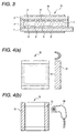
- electrode patterns 3 and 4 are formed on inner surfaces of two insulating base plates 1 and 2 These insulating base plates 1 and 2 are spaced by a prescribed gap and bonded to each other by a sealant 7 on their periphery so that the electrode patterns 3 and 4 are opposite to each other (Fig. 3).
- a liquid crystal material is injected into the prescribed gap to provide a liquid crystal layer 8.
- Polarizing plates 9 and 10 are provided on the outer surfaces of the insulating plates 1 and 2.
- a liquid crystal panel 15 is constructed.
- the feature of the present invention resides in that a light-shielding mask 11 is provided at the edge of the liquid crystal panel from which no electrode pattern is introduced so that it sandwiches the insulating plates 1 and 2 from both sides of the liquid crystal panel.
- the light-shielding mask 11 is preferably formed of a resilient thin metallic plate of phosphor bronze or stainless steel having a thickness of 0.1 - 0.15 mm. This is because these materials can be easily dealt with and can easily interrupt light although it is thin. In order to improve the light-shielding property, the surface of the mask is subjected to lusterless black treatment. Therefore, the mask 11, even if it is very thin, can have sufficient light-shield.
- the black treatment may be ferrite treatment, zinc plating, black coating, etc.
- the thin metallic plate serving as the light mask 11 is bent so that it has a U-shape section with a width of A which is a thickness of the liquid crystal panel (inclusive of the polarizing plates), and its tip is located inside by several degree ( ⁇ ) from the right angle.
- the metallic plate is pushed into the ends of the liquid crystal panel 11 so that it can be easily mounted on the liquid crystal panel 15. Thus, it can be secured to the liquid crystal panel so that it does not easily fall out because of its resiliency.
- an area "D" indicates a display portion.
- the liquid crystal panel 15 has the same configuration as that of a conventional liquid crystal device.
- electrode patterns 3 and 4 which are made of a transparent conductive film of ITO, indium oxide, tin oxide, etc. are provided on the surfaces of insulating base plates 1 and 2 of glass or plastic. These electrode patterns 3 and 4 are patterned using techniques of vacuum evaporation and photolithography. Using the techniques of offset printing of polyimide, orienting films 5 and 6, which determine the arranging direction of molecules of the liquid crystal material, are provided on the surfaces of the electrode patterns 3 and 4. The surfaces of the orienting films 5 and 6 are subjected to rubbing treatment so that the liquid crystal molecules can be easily oriented in a certain direction.
- insulating base plates 1 and 2 are spaced by a prescribed gap through a spacer (not shown) and bonded to each other by a sealant 7 made of an epoxy resin on their periphery so that the electrode patterns 3 and 4 are opposite to each other (Fig. 3).
- a liquid crystal material is injected into the prescribed gap to provide a liquid crystal layer 8.
- Polarizing plates 9 and 10 are provided on the outer surfaces of the insulating plates 1 and 2. In the configuration described above, a liquid crystal panel 15 is constructed.
- the polarizing plates 9 and 10 are provided on the outer surfaces of the insulating base plates 1 and 2 so that their polarizing axes (absorption axes) are in parallel because the polarizing directions are twisted by 90° by the liquid crystal layer 8 which may be made of TN (twist nematic) and configured in the negative type display.
- the liquid crystal layer 8 which may be made of TN (twist nematic) and configured in the negative type display.
- the linear polarized light having passed the one polarizing plate 9 is twisted by 90° by the liquid crystal layer 8 so that it is perpendicular to the polarizing axis of the other polarizing plate 10 and hence interrupted completely.
- the light does not pass to exhibit black.
- the liquid crystal molecules stand up so that the light is not optically rotated by the liquid crystal layer 8.
- the light passes the other polarizing plate 10 as it is, and is recognized as transmitted light.
- the light-shielding mask is only fit in the end of the liquid crystal panel so that the light leaking from the end of the liquid crystal panel, which is attributable to the absence of the liquid crystal layer in the area where the sealant is located, can be completely interrupted. Therefore, in the liquid crystal panel for the negative-type display and large-scale display in which a large number of liquid crystal panels are arranged, the leakage of light from the periphery of the liquid crystal panel or joints therebetween can be disregarded so that the liquid crystal display device with excellent display characteristic can be realized.
- the light-shielding mask can be installed on each liquid crystal panel, in the large-scale display in which a large number of liquid crystal panels are arranged, after the liquid crystal panels have been built into the display, it is not necessary to bond the light shielding tape on each of the joints therebetween. Thus, a large-scale display can be easily realized. Further, replacement of a faulty liquid crystal panel can be also easily performed.
- the embodiment described above was directed to a monochromatic liquid crystal display device.
- the present invention can be more effectively applied to a color liquid display device which is generally in the negative-type display because light does not leak from the periphery of a color display panel.
- the color display device with excellent display characteristic can be realized.
- the liquid crystal display panel was provided with the polarized plates.
- the present invention can be applied to the liquid crystal display panel provided with color filter films instead of the polarized plates.
- the present invention can be applied to a liquid crystal display panel in which first and second base plates having electrode patterns, respectively are bonded with a prescribed gap in their peripheries, a liquid crystal material doped with dichromatic dye is injected in the prescribed gap, a color filter film is provided at the area with no electrode pattern of the first base plate on the front side and another color filter film having the same color is provided at the area with at least the electrode pattern of the second base plate on the rear side.
- Figs. 4A and 4B are views showing the steps in another embodiment according to the present invention.
- a tube of heat-shrinkable resin is prepared as a material of the light-shielding mask 12.
- the heat- shrinkable tube having an internal diameter approximately equal to or slightly larger than the thickness of the liquid crystal panel 15 is cut into two half parts in an axial direction (the section is shown above the light mask 12).
- the part cut from the tube is covered on the end of the liquid crystal panel 15.
- Fig. 4B hot wind is sprayed on the resin by a hot wind blower so that the resin is shrunk.
- terminals of electrode patterns (not shown) are extended in upper and lower directions of the drawing.
- the upper glass plate has a smaller size than that of the lower glass plate so that a level difference is present therebetween.
- the heat- shrinkable tube which has a slightly large diameter may be used.
- the mask covered on the end of the liquid crystal panel with a certain margin, by only spraying hot wind on the mask, the mask can be brought into intimate contact with the end of the liquid crystal panel.
- the liquid crystal display device can be simply completed.
- the mask can be surely fixed on the step.
- a metallic plate or heat-shrinkable tube was used as a light-shielding mask.
- a fitting type mask of resin having the same shape as the metallic plate may be fit in the end of the liquid crystal panel.
- such a mask cannot be made thin unlike the metallic plate, in an application which its thickness is not a serious problem, it can be implemented at lower cost than the metallic plate.
- the gaps between the liquid crystal panels can be stopped up. In this case, it has only to stop up only the narrow areas of the gaps of the liquid crystal panels.
- the display portion of the liquid crystal panel is not covered with the light shielding tape.
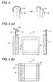
- a light-tight mask 21 is provided with a light-shielding piece 21s which extends outward from the outer edge thereof.
- This embodiment is particularly effective to the case where a plurality of liquid crystal panels are arranged in parallel. This prevents the leakage of light from the gap between the adjacent liquid crystal panels without bonding a light-tight tape.
- Figs. 6A and 6B are views showing the process for implementing this embodiment.
- the light-shielding mask 21 equipped with the light-shielding piece 21s is used.
- the body of the light-shielding mask has a U-shape in section as in the first embodiment.
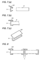
- the light-shielding mask 21 (the section thereof is shown on the upper side), which is formed in the same manner as the light-shielding mask according to the first embodiment shown in Fig. 1, is covered on the end of the liquid crystal panel 15. Subsequently, as seen from Fig. 6B, it is easily mounted on the end of the liquid crystal panel 15 (see Figs. 7A, 7B and 7c). Additionally, as seen from Fig. 6A, a liquid crystal sealing inlet 16 is protruded from the liquid crystal panel.
- the light-shielding mask 21 has a hole H corresponding to the sealing inlet 16. Thus, a gap which leads to leakage of light ⁇ is formed between the adjacent liquid crystal panels. However, the light-shielding piece 21s according to this embodiment covers the gap so that light does not leak from the gap.
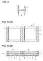
- This embodiment intends to connect two liquid crystal panels using two light-shielding masks which are successively fixed to each other.
- Fig. 9 shows an integral light-mask 11 used in this embodiment.
- the integral light-shielding mask 11 is composed of a first light-shielding mask component and a second light-shielding mask component.
- the shape and material of these light-shielding mask components may be the same as those of the light-shielding mask according to the first embodiment shown in Figs. 1 and 2.
- Figs. 10A and 10B are a top view and sectional view of a liquid crystal panel array in which two liquid crystal panels 15 are coupled with each other using the light-shielding mask 11.
- the adjacent liquid crystal panels can be easily aligned to each other, and coupled with each other with no redundant gap. This configuration is also efficient to eliminate the leakage of light through the gap.
- the leakage of light at the end of the liquid crystal panel can be prevented by a simple structure, thus providing a liquid crystal display device with an excellent display characteristic. Further, where a large number of liquid crystal panels are arranged to constitute a large-scale display, the leakage of light from the joints can be prevented, thereby providing a large-scale display with an excellent display characteristic.
- Electrode patterns 3 and 4 are formed on inner surfaces of two insulating base plates 1 and 2. These two insulating base plates 1 and 2 sandwiches a liquid crystal layer to constitute a liquid crystal panel 15. A light-shielding mask 11 is provided at the end of the liquid crystal panel 15 from which no electrode pattern is introduced so that it sandwiches the insulating plates 1 and 2 from both sides of the liquid crystal panel 15.
Landscapes
- Physics & Mathematics (AREA)
- Nonlinear Science (AREA)
- Mathematical Physics (AREA)
- Chemical & Material Sciences (AREA)
- Crystallography & Structural Chemistry (AREA)
- General Physics & Mathematics (AREA)
- Optics & Photonics (AREA)
- Liquid Crystal (AREA)
- Devices For Indicating Variable Information By Combining Individual Elements (AREA)
Abstract
Description
Claims (19)
- A liquid crystal display device comprisinga liquid crystal panel including two insulating base plates with electrode patterns provided on their surfaces respectively, a sealant which bonds the two insulating base plates to each other at their peripheries with a prescribed gap therebetween so that the electrode patterns are opposite to each other, and a liquid crystal layer provided in the prescribed gap between said two insulating base plates; anda light-shielding mask which is fit in an outer periphery of the sealant at an end of said liquid crystal panel so that it sandwiches said insulating base plates of said liquid crystal panel from both sides.
- A liquid crystal display device according to claim 1, wherein the inner edge of said light-shielding mask is substantially aligned with that of the sealant for the liquid crystal panel.
- A liquid crystal display device according to claim 1, wherein said liquid crystal panel further comprises polarized plates provided outside said first and second insulating base plates, respectively.
- A liquid crystal display device according to claim 1, wherein said light-shielding mask is adapted so that said first and second base plates are fit from both sides.
- A liquid crystal display device according to claim 1, wherein said light-shielding mask has a U-shape in section formed by bending a metallic plate having a light-shielding property and resiliency and having an opening which has an interval slightly smaller than the thickness of the said liquid crystal panel.
- A liquid crystal display device according to claim 1, wherein said light-shielding mask is made of a heat-shrinkable tube of color preventing light from being interrupted.
- A liquid crystal display device according to claim 1, wherein said light-shielding mask is provided on each of both opposite sides of the outer periphery of said liquid crystal panel.
- A liquid crystal display device according to claim 1, wherein said light-shielding mask is provided on each of both opposite sides of the outer periphery of said liquid crystal panel, and on one side located between both opposite sides.
- A liquid crystal display device according to claim 1, wherein said light-shielding mask is provided to cover the entire outer periphery of said liquid crystal panel.
- A liquid crystal display device according to claim 1, wherein said light-shielding mask is provided with a light-shielding piece on at least one side thereof, said light-shielding piece extending outward from the outer edge thereof and serving to interrupt external light from the outer edge of said liquid crystal panel.
- A liquid crystal display device according to claim 1, wherein said light-shielding mask is provided on the outer periphery of said liquid crystal panel and at a coupling portion of two adjacent liquid crystal panels so that said base plates are fit from its both sides.
- A liquid crystal display device according to claim 1, wherein said light-shielding mask includes two light-shielding springs members each having an opening formed in a U-shape in section so as to provide a diameter slightly smaller than the thickness of said liquid crystal panel, said light-shielding spring members being coupled with each other so that their openings are located outside, and two liquid crystal panels are inserted into the corresponding two openings.
- A method of manufacturing a liquid crystal display device comprising the steps of:preparing a liquid crystal panel including two insulating base plates with electrode patterns provided on their surfaces, respectively, a sealant which bonds the two insulating base plates to each other at their peripheries with a prescribed gap therebetween so that the electrode patterns are opposite to each other, and a liquid crystal layer provided in the prescribed gap between said two insulating base plates; andfixing a light-shielding mask which is fit in an outer periphery of the sealant at an end of said liquid crystal panel so that it sandwiches said insulating base plates of said liquid crystal panel from both sides.
- A method of manufacturing a liquid crystal display device according to claim 13, wherein said step of fixing the light-shielding mask comprises the steps:mounting a resilient light shielding tube so that it sandwiches the insulating base plates of said liquid crystal panel from both sides; andheating said light-shielding tube so that it is fit on an outer periphery of the sealant at an end of said liquid crystal panel by heat-shrinkage.
- A method of manufacturing a liquid crystal display device according to claim 13, wherein said step of fixing the light-shielding mask comprises the step of:mounting the insulating base plates of said liquid crystal panel into an opening of a light-shielding spring member formed in a U-shape in section so as to provide a diameter slightly smaller than the thickness of said liquid crystal panel so that the insulating base plates are sandwiched by the light-shielding spring member from both sides.
- A method of manufacturing a liquid crystal display device according to claim 13, wherein said light-shielding mask is made of a heat-shrinkable tube of color preventing light from being interrupted.
- A method of manufacturing a liquid crystal display device according to claim 13, wherein said light-shielding mask is provided on each of both opposite sides of the outer periphery of said liquid crystal panel.
- A method of manufacturing a liquid crystal display device according to claim 13, wherein said step of fixing the light-shielding mask comprises the step of:mounting said light-shielding mask on the outer periphery of said liquid crystal panel and at a coupling portion of two adjacent liquid crystal panels so that said base plates are fit from its both sides, thereby coupling the two adjacent liquid crystal panels.
- A method of manufacturing a liquid crystal display device according to claim 14, wherein said step of fixing the light-shielding mask comprises the step of:preparing an integral light-shielding mask composed of two light-shielding springs members each having an opening formed in a U-shape in section so as to provide a diameter slightly smaller than the thickness of said liquid crystal, said light-shielding spring members being coupled with each other so that their openings are located outside;inserting two liquid crystal panels into the corresponding two openings so that they are coupled with each other.
Applications Claiming Priority (2)
| Application Number | Priority Date | Filing Date | Title |
|---|---|---|---|
| JP25716998 | 1998-09-10 | ||
| JP25716998 | 1998-09-10 |
Publications (3)
| Publication Number | Publication Date |
|---|---|
| EP0985951A2 true EP0985951A2 (en) | 2000-03-15 |
| EP0985951A3 EP0985951A3 (en) | 2004-02-04 |
| EP0985951B1 EP0985951B1 (en) | 2005-11-30 |
Family
ID=17302654
Family Applications (1)
| Application Number | Title | Priority Date | Filing Date |
|---|---|---|---|
| EP99117778A Expired - Lifetime EP0985951B1 (en) | 1998-09-10 | 1999-09-09 | Liquid crystal display device and method of fabricating thereof |
Country Status (5)
| Country | Link |
|---|---|
| US (1) | US6337727B1 (en) |
| EP (1) | EP0985951B1 (en) |
| CN (1) | CN1126977C (en) |
| CA (1) | CA2282046A1 (en) |
| DE (1) | DE69928620T2 (en) |
Cited By (3)
| Publication number | Priority date | Publication date | Assignee | Title |
|---|---|---|---|---|
| EP1209513A3 (en) * | 2000-11-22 | 2003-07-30 | Seiko Epson Corporation | Liquid crystal display device and electronic apparatus provided with the same |
| EP1457811A1 (en) * | 2003-02-28 | 2004-09-15 | EM Microelectronic-Marin SA | Negative-type display device with uniform colour and method of producing such a device |
| US10698246B2 (en) | 2015-04-20 | 2020-06-30 | Guangdong Oppo Mobile Telecommunications Corp., Ltd. | Display screen, display screen assembly, and terminal |
Families Citing this family (20)
| Publication number | Priority date | Publication date | Assignee | Title |
|---|---|---|---|---|
| KR100830524B1 (en) * | 2001-12-29 | 2008-05-21 | 엘지디스플레이 주식회사 | Light leakage prevention structure of liquid crystal display |
| WO2003077019A1 (en) * | 2002-03-14 | 2003-09-18 | Nec Corporation | Optical modulating/displaying device and production method therefor and display apparatus mounting the optical modulating/displaying device thereon |
| US7698833B2 (en) * | 2002-03-15 | 2010-04-20 | Lg Display Co., Ltd. | Apparatus for hardening a sealant located between a pair bonded substrates of liquid crystal display device |
| JP2004004563A (en) * | 2002-03-27 | 2004-01-08 | Fujitsu Display Technologies Corp | Liquid crystal display substrate, liquid crystal display device having the same, method of manufacturing the same, and manufacturing apparatus |
| JP3772888B2 (en) * | 2003-05-02 | 2006-05-10 | セイコーエプソン株式会社 | Electro-optical device and electronic apparatus |
| JP4421868B2 (en) * | 2003-10-10 | 2010-02-24 | キヤノンアネルバ株式会社 | Manufacturing method of liquid crystal panel and gap adjusting device |
| CN100562887C (en) * | 2004-05-13 | 2009-11-25 | 统宝光电股份有限公司 | Touch panel with shading structure |
| CN100334495C (en) * | 2004-06-30 | 2007-08-29 | 友达光电股份有限公司 | Frame glue repair method |
| DE202005005307U1 (en) * | 2005-04-04 | 2006-08-10 | Aeg Gesellschaft für Moderne Informationssysteme mbH | A liquid crystal display element and a liquid crystal display device comprising a plurality of such liquid crystal display elements |
| CN100543565C (en) * | 2006-11-28 | 2009-09-23 | 友达光电股份有限公司 | LCD panel |
| EP2381755B1 (en) * | 2010-04-26 | 2015-11-04 | LG Electronics Inc. | Multi display device |
| US8804090B2 (en) * | 2010-12-02 | 2014-08-12 | Lawrence E. Tannas, Jr. | Methods for creating a minimally visible seal along the edge of a flat panel display |
| KR20120062283A (en) * | 2010-12-06 | 2012-06-14 | 삼성모바일디스플레이주식회사 | An liquid crystal display device and the manufacturing method thereof |
| TWI457656B (en) * | 2011-11-29 | 2014-10-21 | Au Optronics Corp | Optical display panel, panel display module, and method of forming light-blocking structure |
| KR101874954B1 (en) * | 2012-01-19 | 2018-07-06 | 삼성디스플레이 주식회사 | Multi display device |
| CN104204122A (en) * | 2012-03-30 | 2014-12-10 | 早川橡胶株式会社 | Method for separating member using laser light |
| CN102636906B (en) * | 2012-05-09 | 2015-07-15 | 深圳市华星光电技术有限公司 | Optical diaphragm of liquid crystal display device and liquid crystal display device |
| CN108136747B (en) * | 2015-09-30 | 2020-02-18 | 富士胶片株式会社 | Manufacturing method of three-dimensional fluid unit |
| CN107577090B (en) * | 2017-09-26 | 2021-02-19 | 京东方科技集团股份有限公司 | Display panel, manufacturing method thereof and display device |
| CN108169998B (en) * | 2018-01-03 | 2021-01-08 | 京东方科技集团股份有限公司 | Mask plate, use method thereof and exposure equipment |
Family Cites Families (7)
| Publication number | Priority date | Publication date | Assignee | Title |
|---|---|---|---|---|
| JPH03282427A (en) * | 1990-03-29 | 1991-12-12 | Ricoh Co Ltd | Liquid crystal display element |
| US5169693A (en) * | 1990-03-29 | 1992-12-08 | Ricoh Company, Ltd. | Liquid crystal display element |
| US5455696A (en) * | 1992-07-10 | 1995-10-03 | Kabushiki Kaisha Topcon | Display apparatus including a liquid and two plates bonded together by a fluorocarbon resin |
| JPH06186539A (en) * | 1992-10-13 | 1994-07-08 | Afuiniteii Kk | Laminate |
| JPH09258203A (en) * | 1996-03-19 | 1997-10-03 | Hitachi Ltd | Liquid crystal display |
| US5661531A (en) * | 1996-01-29 | 1997-08-26 | Rainbow Displays Inc. | Tiled, flat-panel display having invisible seams |
| JPH1051713A (en) * | 1996-08-02 | 1998-02-20 | Mitsubishi Electric Corp | Projection Television Display Holder |
-
1999
- 1999-09-08 CA CA002282046A patent/CA2282046A1/en not_active Abandoned
- 1999-09-09 US US09/392,631 patent/US6337727B1/en not_active Expired - Fee Related
- 1999-09-09 DE DE69928620T patent/DE69928620T2/en not_active Expired - Fee Related
- 1999-09-09 EP EP99117778A patent/EP0985951B1/en not_active Expired - Lifetime
- 1999-09-10 CN CN99118646A patent/CN1126977C/en not_active Expired - Fee Related
Cited By (3)
| Publication number | Priority date | Publication date | Assignee | Title |
|---|---|---|---|---|
| EP1209513A3 (en) * | 2000-11-22 | 2003-07-30 | Seiko Epson Corporation | Liquid crystal display device and electronic apparatus provided with the same |
| EP1457811A1 (en) * | 2003-02-28 | 2004-09-15 | EM Microelectronic-Marin SA | Negative-type display device with uniform colour and method of producing such a device |
| US10698246B2 (en) | 2015-04-20 | 2020-06-30 | Guangdong Oppo Mobile Telecommunications Corp., Ltd. | Display screen, display screen assembly, and terminal |
Also Published As
| Publication number | Publication date |
|---|---|
| US6337727B1 (en) | 2002-01-08 |
| CN1126977C (en) | 2003-11-05 |
| CN1248713A (en) | 2000-03-29 |
| DE69928620T2 (en) | 2006-07-20 |
| CA2282046A1 (en) | 2000-03-10 |
| DE69928620D1 (en) | 2006-01-05 |
| EP0985951B1 (en) | 2005-11-30 |
| EP0985951A3 (en) | 2004-02-04 |
Similar Documents
| Publication | Publication Date | Title |
|---|---|---|
| US6337727B1 (en) | Liquid crystal display device and method of fabricating thereof | |
| JP4177658B2 (en) | Liquid crystal display | |
| US6573957B1 (en) | Liquid crystal display device | |
| US5796451A (en) | Liquid crystal cell with an external color filter | |
| JP2991407B2 (en) | Liquid crystal display device and method of manufacturing the same | |
| JP3512665B2 (en) | Color liquid crystal panel and manufacturing method thereof | |
| KR960025293A (en) | Liquid crystal display panel and liquid crystal display device | |
| JP2001305561A (en) | Liquid crystal display | |
| WO2007086166A1 (en) | Liquid crystal display device and television receiver | |
| US6335774B1 (en) | Liquid crystal display device and method of fabricating thereof | |
| JP2569548B2 (en) | Projection display device | |
| JP2968987B2 (en) | LCD display | |
| JP2000147473A (en) | Liquid crystal display element and its production | |
| JP3777307B2 (en) | Liquid crystal display | |
| JP3718252B2 (en) | Manufacturing method of liquid crystal display panel | |
| JP2785808B2 (en) | Liquid crystal panel and projection display | |
| JP2000089207A (en) | Liquid crystal display device | |
| JPH10333158A (en) | Liquid crystal display device | |
| JPH04296826A (en) | Liquid crystal display device | |
| JP2003161948A (en) | Liquid crystal display | |
| KR20030042641A (en) | Liquid crystal display having conductive pillar | |
| JPH09101544A (en) | Liquid crystal display | |
| JPH0259999B2 (en) | ||
| JPH05134240A (en) | Negative type liquid crystal display element | |
| JPH0358023A (en) | Liquid crystal display element and its production |
Legal Events
| Date | Code | Title | Description |
|---|---|---|---|
| PUAI | Public reference made under article 153(3) epc to a published international application that has entered the european phase |
Free format text: ORIGINAL CODE: 0009012 |
|
| AK | Designated contracting states |
Kind code of ref document: A2 Designated state(s): AT BE CH CY DE DK ES FI FR GB GR IE IT LI LU MC NL PT SE |
|
| AX | Request for extension of the european patent |
Free format text: AL;LT;LV;MK;RO;SI |
|
| PUAL | Search report despatched |
Free format text: ORIGINAL CODE: 0009013 |
|
| AK | Designated contracting states |
Kind code of ref document: A3 Designated state(s): AT BE CH CY DE DK ES FI FR GB GR IE IT LI LU MC NL PT SE |
|
| AX | Request for extension of the european patent |
Extension state: AL LT LV MK RO SI |
|
| RIC1 | Information provided on ipc code assigned before grant |
Ipc: 7G 02F 1/1335 A |
|
| 17P | Request for examination filed |
Effective date: 20040322 |
|
| 17Q | First examination report despatched |
Effective date: 20040428 |
|
| AKX | Designation fees paid |
Designated state(s): DE FR GB |
|
| GRAP | Despatch of communication of intention to grant a patent |
Free format text: ORIGINAL CODE: EPIDOSNIGR1 |
|
| GRAS | Grant fee paid |
Free format text: ORIGINAL CODE: EPIDOSNIGR3 |
|
| GRAA | (expected) grant |
Free format text: ORIGINAL CODE: 0009210 |
|
| AK | Designated contracting states |
Kind code of ref document: B1 Designated state(s): DE FR GB |
|
| REG | Reference to a national code |
Ref country code: GB Ref legal event code: FG4D |
|
| REF | Corresponds to: |
Ref document number: 69928620 Country of ref document: DE Date of ref document: 20060105 Kind code of ref document: P |
|
| ET | Fr: translation filed | ||
| PLBE | No opposition filed within time limit |
Free format text: ORIGINAL CODE: 0009261 |
|
| STAA | Information on the status of an ep patent application or granted ep patent |
Free format text: STATUS: NO OPPOSITION FILED WITHIN TIME LIMIT |
|
| 26N | No opposition filed |
Effective date: 20060831 |
|
| PGFP | Annual fee paid to national office [announced via postgrant information from national office to epo] |
Ref country code: FR Payment date: 20080915 Year of fee payment: 10 |
|
| PGFP | Annual fee paid to national office [announced via postgrant information from national office to epo] |
Ref country code: GB Payment date: 20080910 Year of fee payment: 10 |
|
| PGFP | Annual fee paid to national office [announced via postgrant information from national office to epo] |
Ref country code: DE Payment date: 20080926 Year of fee payment: 10 |
|
| GBPC | Gb: european patent ceased through non-payment of renewal fee |
Effective date: 20090909 |
|
| REG | Reference to a national code |
Ref country code: FR Ref legal event code: ST Effective date: 20100531 |
|
| PG25 | Lapsed in a contracting state [announced via postgrant information from national office to epo] |
Ref country code: FR Free format text: LAPSE BECAUSE OF NON-PAYMENT OF DUE FEES Effective date: 20090930 Ref country code: DE Free format text: LAPSE BECAUSE OF NON-PAYMENT OF DUE FEES Effective date: 20100401 |
|
| PG25 | Lapsed in a contracting state [announced via postgrant information from national office to epo] |
Ref country code: GB Free format text: LAPSE BECAUSE OF NON-PAYMENT OF DUE FEES Effective date: 20090909 |