BACKGROUND OF THE INVENTION
TECHNICAL ART
-
The present invention relates generally to an organic
EL (electroluminescent) device, and more specifically to
an inorganic/organic junction structure used for a device
comprising an organic compound thin film which emits light
at an applied electric field.
BACKGROUND ART
-
In general, an organic EL device is basically built
up of an ITO or other transparent electrode formed on a
glass substrate, an organic amine base hole transporting
layer laminated on the transparent electrode, an organic
light emitting layer formed of a material having
electronic conductivity and giving out strong light
emission, for instance, an Alq3 material, and an electrode
provided on the organic light emitting layer and formed of
a material having a low work function, for instance, an
MgAg material.
-
As reported so far in the art, the device has a
structure wherein one or plural organic compound layers
are interleaved between a hole injecting electrode and an
electron injecting electrode. The organic compound layer
has a double- or triple-layer structure.
-
Examples of the double-layer structure are a
structure wherein a hole transporting layer and a light
emitting layer are formed between the hole injecting
electrode and the electron injecting electrode, and a
structure wherein a light emitting layer and an electron
transporting layer are formed between the hole injecting
electrode and the electron injecting electrode. In an
exemplary triple-layer structure, a hole transporting
layer, a light emitting layer and an electron transporting
layer are provided between the hole injecting electrode
and the electron injecting electrode. A single-layer
structure wherein a single layer has all functions, too,
is reported in conjunction with a polymer or mixture
system.
-
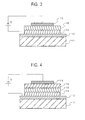
Typical structures of the organic EL device are shown
in Figures 3 and 4.
-
In Fig. 3, a hole transporting layer 14 and a light
emitting layer 15, each made of an organic compound, are
formed between a hole injecting electrode 12 provided on a
substrate 11 and an electron injecting electrode 13. In
this case, the light emitting layer 15 also functions as
an electron transporting layer.
-
In Fig. 4, a hole transporting layer 14, a light
emitting layer 15 and an electron transporting layer 16,
each made of an organic compound, are formed between a
hole injecting electrode 12 provided on a substrate 11 and
an electron injecting electrode 13.
-
A problem common to these organic EL devices is
reliability. In principle, an organic EL device comprises
a hole injecting electrode and an electron injecting
electrode and requires an organic layer for efficient
injection and transportation of holes and electrons from
between these electrodes. However, these materials are
sensitive to damages during device fabrication, and offer
a problem in conjunction with an affinity for electrodes.
Another problem is that the deterioration of an organic
thin film is much severer than that of an LED or LD.
-
Most organic materials are relatively expensive.
Otherwise stated, there is a great merit in providing low-cost
organic EL device products by substituting a partial
constitution film with an inexpensive inorganic material.
-
Furthermore, the development of a device having
higher light emission efficiency, lower driving voltage
and lesser power consumption than ever before is strongly
desired.
-
To provide a solution to such problems, methods of
taking advantage of merits of both an organic material and
an inorganic semiconductor material have been envisaged.
That is, an organic/inorganic semiconductor junction
structure wherein an organic hole transporting layer is
substituted by an inorganic p-type semiconductor has been
contemplated. Such contemplation has been investigated in
Japanese Patent No. 2636341, and JP-A's 2-139893, 2-207488
and 6-119973. However, it is still difficult to obtain an
organic EL device superior to prior art organic ELs in
terms of emission performance and basic device reliability.
SUMMARY OF THE INVENTION
-
One object of the invention is to provide an organic
EL device which possesses the merits of both an organic
material and an inorganic material, has an extended life,
an improved light emission efficiency, a low driving
voltage and high luminance, and is fabricated at low cost.
-
Another object of the invention is to provide an
organic EL device having practically great value in high-performance
flat color display applications.
-
The above object is achieved by the inventions
defined below.
-
(1) An organic EL device comprising a substrate, a
hole injecting electrode and a cathode formed on said
substrate, and at least one organic layer located between
these electrodes, wherein:
- an inorganic insulating electron injecting layer is
located between said cathode and said organic layer,
- said inorganic insulating electron injecting layer
comprising:
- as an oxide having a low work function at least one
oxide having a work function of lower than 2.5 eV, and
- as an oxide having a high work function at least one
oxide having a work function of 2.5 to 4 eV.
-
-
(2) The organic EL device according to (1), wherein
said oxide having a low work function is at least one
oxide selected from the group consisting of lithium oxide,
sodium oxide, potassium oxide, rubidium oxide, cesium
oxide, calcium oxide, strontium oxide, barium oxide, and
yttrium oxide.
-
(3) The organic EL device according to (1), wherein
said oxide having a high work function is at least one
oxide selected from the group consisting of beryllium
oxide, magnesium oxide, titanium oxide, iron oxide,
zirconium oxide, hafnium oxide, lanthanum oxide, cerium
oxide, praseodymium oxide, neodymium oxide, samarium oxide,
europium oxide, gadolinium oxide, terbium oxide,
dysprosium oxide, holmium oxide, erbium oxide, ytterbium
oxide, lutetium oxide, and thorium oxide.
-
(4) The organic EL device according to (1), wherein
said inorganic insulating electron injecting layer
contains 5 to 50 mol% of said oxide having a high work
function.
-
(5) The organic EL device according to (1), wherein
a work function difference between said oxide having a low
work function and said oxide having a high work function
is 0.5 to 2.5 eV.
-
(6) The organic EL device according to (1), wherein
said inorganic insulating electron injecting layer has a
band gap of at least 4 eV.
-
(7) The organic EL device according to (1), wherein
said inorganic insulating electron injecting layer has a
structure where said oxide having a low work function is
present in a large amount on an organic layer side and
said oxide having a high work function is present in a
large amount on a cathode side.
-
(8) The organic EL device according to (1), wherein
said cathode comprises aluminum as a main component.
BRIEF DESCRIPTION OF THE DRAWINGS
-
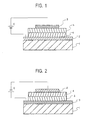
Figure 1 is a sectional schematic of one embodiment
of the organic EL device according to the Invention.
-
Figure 2 is a sectional schematic of another
embodiment of the organic EL device according to the
invention.
-
Figure 3 is a sectional view of an organic EL device
comprising a hole transporting layer and having a double-layer
structure.
-
Figure 4 is a sectional view of an organic EL device
comprising a hole transporting layer and an electron
transporting layer and having a triple-layer structure.
DETAILED EXPLANATION OF THE PREFERRED EMBODIMENTS
-
The organic EL device of the invention comprises a
substrate, a hole injecting electrode and a cathode formed
on the substrate, and at least one organic layer located
between these electrodes, wherein between said cathode and
said organic layer there is provided an inorganic
insulating electron injecting layer. The inorganic
insulating electron injecting layer comprises as an oxide
having a low work function at least one oxide having a
work function of lower than 2.5 eV and as an oxide having
a high work function at least one oxide having a work
function of 2.5 to 4 eV.
-
The "work function" is by definition the magnitude of
the minimum work needed for extracting electrons from a
solid in a vacuum, and corresponds to the depth of a solid
Fermi level measured on the basis of a rest free electron
level in a vacuum. Electrons migrate from a metal having
a low work function toward a metal having a high work
function via the tunnel effect.
-
In the invention, the inorganic insulting electron
injecting layer contains both the oxide having a work
function of lower than 2.5 eV and the oxide having a work
function of 2.5 to 4 eV, so that electrons can be
efficiently injected from the cathode into the organic
layers such as the electron transporting layer and the
light emitting layer, resulting in an emission luminance
improvement. That is, by the incorporation of the oxide
having a high work function found between the work
function of the oxide having a low work function of lower
than 2.5 eV and that of the electron injecting electrode
in the electron injecting layer, the electrons migrate to
the oxide having a low work function and the organic
layers via the oxide having a high work function, so that
the energy barrier at a single stage can be reduced to
facilitate injection of the electrons into the light
emitting layer. It is also possible to use for the
cathode a material having a high work function of about
4.4 eV (4.41 to 4.06 eV), for instance, Al. By allowing
the electron injecting layer to have such composition, the
migration of holes from the organic layer side to the
electron injecting layer can be blocked at their interface,
leading to efficient recombination of holes and electrons
in the light emitting layer. In addition, the organic EL
device can have both the merits of the inorganic material
such as weather resistance and heat resistance and the
merits of the organic material such as a high degree of
design flexibility.
-
The inorganic insulating electron injecting layer
contains as the oxide having a low work function an oxide
having a work function of lower than 2.5 eV, and
preferably 0.5 to 2.3 eV. Such an oxide, for instance,
includes lithium oxide (Li2O), sodium oxide (Na2O),
potassium oxide (K2O), rubidium oxide (Rb2O), cesium oxide
(Cs2O), calcium oxide (CaO), strontium oxide (SrO), barium
oxide (BaO), and yttrium oxide (Y2O3), among which
strontium oxide, and lithium oxide are particularly
preferred. These oxides may be used singly or in
combination of two or more. It is here to be noted that
the oxides may deviate somewhat from their stoichiometric
compositions although they are usually found therewith.
-
In addition, the inorganic insulating electron
injecting layer contains as the oxide having a high work
function an oxide having a work function of 2.5 to 4 eV,
preferably 2.5 to 3.5 eV, and more preferably 2.8 to 3.5
eV. Such an oxide, for instance, includes beryllium oxide
(BeO), magnesium oxide (MgO), titanium oxide (TiO, TiO2),
iron oxide (FeO), zirconium oxide (ZrO2), hafnium oxide
(HfO2), lanthanum oxide (La2O3), cerium oxide (Ce2O3),
praseodymium oxide (Pr2O3), neodymium oxide (Nd2O3),
samarium oxide (Sm2O3), europium oxide (Eu2O3), gadolinium
oxide (Gd2O3), terbium oxide (Tb2O3), dysprosium oxide
(Dy2O3), holmium oxide (Ho2O3), erbium oxide (Er2O3),
ytterbium oxide (Yb2O3), lutetium oxide (Lu2O3), and
thorium oxide (ThO2), among which cerium oxide, and
hafnium oxide are particularly preferred. These oxides
may be used singly or in combination of two or more. It
is here to be noted that the oxides may deviate somewhat
from their stoichiometric compositions although they are
usually found therewith.
-
The oxide having a high work function of 2.5 to 4 eV
should preferably account for 5 to 50 mol%, and especially
10 to 40 mol%, of the inorganic insulating electron
injecting layer. Any deviation from this content range
incurs an electron injection capability drop and an
emission luminance drop.
-
In the invention, the best selection should be made
from combinations of the oxide having a low work function
with the oxide having a high work function while the work
functions of the electron injecting electrode used and the
organic layers used, e.g., the light emitting layer are
taken into consideration. In short, if the work function
of the oxide having a high work function comes in between
the work function of the oxide having a low work function
and the work function of the electron injecting electrode,
the energy barrier can then be minimized. For instance,
it is preferable to use Al (having a work function of 4.4
eV) for the electron injecting electrode, SrO (having a
work function of 1.3 eV) as the oxide having a low work
function for the electron injecting layer, and HfO2
(having a work function of 2.8 eV) as the oxide having a
high work function. Preferably, the work function
difference between the oxide having a low work function
and the oxide having a high work function should be 0.5 to
2.5 eV, and especially 1 to 2 eV.
-
In the inorganic insulating electron injecting layer,
the oxide having a low work function may be uniformly
mixed with the oxide having a high work function. However,
the inorganic insulating electron injecting layer should
preferably have a structure wherein the oxide having a low
work function is present in a large amount on the organic
layer side and the oxide having a high work function is
present in s large amount on the cathode side. Such a
structure enables electrons to be efficiently injected
from the cathode into the light emitting layer, so that a
further improvement in luminance can be obtained.
-
The inorganic insulating electron injecting layer
should preferably have a band gap of at least 4 eV,
especially at least 5 eV, and more especially at least 6
eV. Preferably but not exclusively, the upper limit to
the band gap is usually of the order of 8 eV. The
electron affinity should preferably be of the order of 2.5
to 3.5 eV.
-
The values of the work function and band gap are
determined by a thin-film structure and a thin-film
constituting material. The work function may be measured
as by X-ray photoelectron spectrometry (XPS) harnessing
photoemission, and the band gap value may be measured as
by spectrometry.
-
The inorganic insulating electron injecting layer is
usually in a noncrystalline state.
-
Preferably but not exclusively, the inorganic
insulating electron injecting layer should have a
thickness of the order of 0.2 to 10 nm, and especially 1
to 10 nm.
-
The inorganic insulating electron injecting layer may
be fabricated by various physical or chemical thin-film
formation processes such as a sputtering process, and an
EB evaporation process, with the sputtering process being
preferred.
-
When the inorganic insulating electron injecting
layer is formed by the sputtering process, it is
preferable that the pressure of the sputtering gas during
sputtering is in the range of 0.1 to 1 Pa. For the
sputtering gas, inert gases used with an ordinary
sputtering system, for instance, Ar, Ne, Xe, and Kr may be
used. If required, N2 may be used. Use may then be made
of a sputtering atmosphere comprising a mixture of the
sputtering gas with about 1 to 99% of O2. A single- or
multi-stage sputtering process may be performed using the
aforesaid oxide or oxides for a target or targets.
-
When there is a fear that the organic layers, etc.
may be ashed and so damaged during the lamination of the
inorganic insulating electron injecting layer, it is
preferable to divide the inorganic insulating electron
injecting layer to two layers before lamination. That is,
the first layer is laminated thin with no addition of
oxygen thereto, and the second layer is then laminated
thick with the addition of oxygen thereto. In this case,
the first layer with no oxygen added thereto should have a
thickness that is about 1/5 to 4/5 of the total thickness.
At this time, the oxygen-deficient layer formed with no
addition of oxygen thereto should preferably an oxygen
content of the order of 60 to 90%. The oxide layer formed
with the addition of oxygen thereto is usually present
with stoichiometric composition for an ordinary oxide.
However, the oxide layer composition may deviate somewhat
from the stoichiometric composition. Accordingly, the
difference in oxygen content between the oxygen-deficient
layer and the oxidized layer should preferably be at least
10%, and especially at least 20%. Alternatively, the
oxygen content may change continuously in the above range.
-
For the sputtering process, an RF sputtering process
using an RF power source, a DC sputtering process, etc.
may be used, with the RF sputtering process being most
preferred. Power for a sputtering system is preferably in
the range of 0.1 to 10 W/cm2 for RF sputtering, and the
film formation rate is preferably in the range of 0.5 to
50 nm/min., and especially 1 to 5 nm/min.
-
During film formation, the temperature of the
substrate is about room temperature (25°C) to 150°C.
-
For the cathode (electron injecting electrode)
material, for instance, mention may be made of pure metal
elements such as K, Li, Na, Mg, La, Ce, Ca, Sr, Ba, Al, Ag,
In, Sn, Zn, and Zr, and a binary or ternary alloy system
serving as a stabilier improver and containing these
elements, e.g., Ag·Mg (Ag: 0.1 to 50 at%), Al·Li (Li: 0.01
to 12 at%), In·Mg (Mg: 50 to 80 at%), and Al·Ca (Ca: 0.01
to 20 at%). In the organic EL device of the invention,
the electron injecting layer contains both the oxide
having a high work function and the oxide having a low
work function, so that the energy barrier at a single
stage can be reduced, and so a substance having a high
work function can also be suitable for the cathode. By
use of Al it is thus possible to obtain sufficiently high
electron injection efficiency. For the cathode material,
it is particularly preferable to use Al having a high work
function yet low resistance or an alloy containing at
least 90 at% of Al. For the cathode layer, a thin film
made up of each of these materials, and a multilayer thin
film made of two or more such materials may be used.
-
The cathode thin film should preferably have at least
a certain thickness enough to inject electrons or a
thickness of at least 0.1 nm, preferably at least 0.5 nm,
and more preferably at least 1 nm. Although there is no
particular upper limit to the cathode thickness, the
cathode may usually have a thickness of the order of 1 to
500 nm. Additionally, an auxiliary electrode (protective
electrode) may be located on the cathode.
-
The auxiliary electrode should preferably have at
least a certain thickness enough to ensure electron
injection efficiency and prevent entrance of moisture,
oxygen or organic solvents or a thickness of preferably at
least 50 nm, more preferably at least 100 mm, and even
more preferably 100 to 500 nm. With too thin an auxiliary
electrode, neither is its own effect obtainable, nor is
sufficient connection with terminal electrodes obtainable
because the ability of the auxiliary electrode to cover
steps becomes low. When the auxiliary electrode is too
thick, on the other hand, the growth rate of dark spots
becomes high because of an increase in the stress of the
auxiliary electrode.
-
The auxiliary electrode should preferably be formed
of the optimum material chosen depending on the cathode
material used in combination therewith. For instance, a
low-resistance metal such as Al may be used if it is
important to make up for low electron injection efficiency
of the cathode, and a metal compound such as TiN may be
used if emphasis is placed on sealability. In the
invention, however, it is not always necessary to use the
auxiliary electrode because the use of Al as the cathode
ensures sufficient electron injection efficiency.
-
Preferably but not exclusively, the total thickness
of the cathode plus the auxiliary electrode should usually
be the order of 50 to 500 nm.
-
The hole injecting electrode should preferably be
composed of a material that can inject holes in the hole
injecting layer with high efficiency and has a work
function of 4.5 eV to 5.5 eV, for instance, any one of
tin-doped indium oxide (ITO), zinc-doped indium oxide
(IZO), indium oxide (In2O3), tin oxide (SnO2), and zinc
oxide (ZnO). It is here to be noted that these oxides may
deviate slightly from their stoichiometric compositions.
Regarding ITO, it is desired that the mixing ratio of SnO2
with respect to In2O3 be in the range of 1 to 20 wt%, and
especially 5 to 12 wt%. Regarding IZO, the mixing ratio
of ZnO with respect to In2O3 is usually in the range of 12
to 32 wt%.
-
The hole injecting electrode may further contain
silicon oxide (SIO2) for work function control. The
content of silicon oxide (SiO2) should preferably be of
the order of 0.5 to 10% in terms of the molar ratio of
SiO2 to ITO. The incorporation of SiO2 contributes to an
increase in the work function of ITO.
-
The electrode on the side out of which light is taken
should preferably have a light transmittance of at least
80%, and more especially at least 90% with respect to
light emitted at an emission wavelength of usually 400 to
700 nm. With decreasing transmittance, the light emitted
from the light emitting layer attenuates, and so it is
difficult to obtain the luminance needed for an light
emitting device.
-
The electrode should preferably have a thickness of
50 to 500 nm, and especially 50 to 300 nm. Although there
is no particular upper limit to the electrode thickness,
too thick an electrode gives rise to concerns such as a
transmittance drop, and defoliation. Too thin an
electrode fails to obtain sufficient effect, and offers a
problem in conjunction with film thickness, etc. during
device fabrication.
-
One embodiment of the organic EL device of the
invention should preferably have a multilayer structure
reverse to an ordinary multilayer structure (a hole
injecting layer is located on the substrate side), which
comprises, in order from a substrate 1, a cathode 2, an
inorganic insulating electron injecting layer 4, a light
emitting layer 5 and a hole injecting electrode 3
laminated together on the substrate 1, as typically shown
in Fig. 1. The reversed multilayer structure makes it
possible to prevent damage to the organic layers due to
ashing during the formation of the inorganic insulating
electron injecting layer. As typically shown in Fig. 2, a
multilayer structure comprising, in order from a substrate
1, a hole injecting electrode 3, a light emitting layer 5,
an inorganic insulating electron injecting layer 4 and a
cathode 2 laminated together on the substrate 1 is also
acceptable. Preferably in this case, the inorganic
insulating electron injecting layer should have such a
double-layer structure as already noted. These
embodiments may be properly chosen depending on display
fabrication processes, etc. In Figs. 1 and 2, a driving
power source E is connected between the hole injecting
electrode 2 and the cathode 3. The term "light emitting
layer" 5 is here understood to refer to a light emitting
layer in a broad sense and so encompass a hole injecting
and transporting layer, a light emitting layer in a narrow
sense, an electron transporting layer, etc.
-
In the device according to the invention, layer units
such as an electrode layer/inorganic layer (inorganic
insulating electron injecting layer), a light emitting
layer/electrode layer/inorganic layer, a light emitting
layer/electrode layer/inorganic layer, a light emitting
layer/electrode layer, and so on may be cascaded one upon
another. Such a device structure enables color tone
control of emitted light, and multicolor light emission.
-
The light emitting layer is made up by lamination of
one or two or more organic compound thin films taking part
in at least a light emission function.
-
The light emitting layer has functions of injecting
holes and electrons, transporting them, and recombining
holes and electrons to create excitons. For the light
emitting layer, it is preferable to use a relatively
electronically neutral compound, so that the electrons and
holes can be easily injected and transported in a well-balanced
state.
-
If required, the light emitting layer may contain in
addition to the light emitting layer in a narrow sense a
hole injecting and transporting layer, an electron
transporting layer, etc.
-
The hole injecting and transporting layer has
functions of facilitating injection of holes from the hole
injecting electrode, providing stable transportation of
holes and blocking electrons. The electron transporting
layer, provided as occasion demands, has functions of
facilitating injection of electrons from the inorganic
insulating electron injecting layer, providing stable
transportation of electrons and blocking holes. These
layers are effective for increasing the number of holes
and electrons injected into the light emitting layer and
confining holes and electrons therein for optimizing the
recombination region to improve light emission efficiency.
-
Preferably but not exclusively, the thickness of the
light emitting layer, the thickness of the hole injecting
and transporting layer, and the thickness of the electron
transporting layer should preferably be of the order of
usually 5 to 500 nm, and especially 10 to 300 nm although
varying depending on their formation processes.
-
The thickness of the hole injecting and transporting
layer, and the electron transporting layer is
approximately equal to, or ranges from about 1/10 times to
about 10 times, the thickness of the light emitting layer
although it depends on the design of the
recombination/light emitting region. When the hole
injecting and transporting layer is separated into an
injecting layer and a transporting layer, it is preferable
that the injecting layer is at least 1 nm thick and the
transporting layer is at least 1 nm thick. The upper
limit to thickness is usually about 500 nm for the
injecting layer and about 500 nm for the transporting
layer. The same film thickness is also true of the case
where two injecting and transporting layers are provided.
-
In the organic EL device according to the invention,
the light emitting layer contains a fluorescent material
that is a compound capable of emitting light. The
fluorescent material used herein, for instance, may be at
least one compound selected from compounds such as those
disclosed in JP-A 63-264692, e.g., quinacridone, rubrene,
and styryl dyes. Use may also be made of quinoline
derivatives such as metal complex dyes containing 8-quinolinol
or its derivative as ligands, for instance,
tris(8-quinolinolato)aluminum, tetrapheny[butadiene,
anthracene, perylene, coronene, and 12-phthaloperinone
derivatives. Use may further be made of phenylanthracene
derivatives disclosed in JP-A 8-12600 (Japanese Patent
Application No. 6-110569) and tetraarylethene derivatives
disclosed in JP-A 8-12969 (Japanese Patent Application No.
6-114456).
-
Preferably, the fluorescent compound is used in
combination with a host substance capable of emitting
light by itself; that is, it is preferable that the
fluorescent compound is used as a dopant. In such a case,
the content of the fluorescent compound in the light
emitting layer is in the range of preferably 0.01 to 10%
by weight, and especially 0.1 to 5% by weight. By using
the fluorescent compound in combination with the host
substance, it is possible to vary the wavelength
performance of light emission of the host substance,
thereby making light emission possible on a longer
wavelength side and, hence, improving the light emission
efficiency and stability of the device.
-
Quinolinolato complexes, and aluminum complexes
containing 8-quinolinol or its derivatives as ligands are
preferred for the host substance. Such aluminum complexes
are typically disclosed in JP-A's 63-264692, 3-255190, 5-70733,
5-258859, 6-215874, etc.
-
Exemplary aluminum complexes include tris(8-quinolinolato)aluminum,
bis(8-quinolinolato)magnesium,
bis(benzo{f}-8-quinolinolato)zinc, bis(2-methyl-8-quinolinolato)aluminum
oxide, tris(8-quinolinolato)indium,
tris(5-methyl-8-quinolinolato)aluminum, 8-quinolinolato-lithium,
tris(5-chloro-8-quinolinolato)gallium, bis(5-chloro-8-quinolinolato)calcium,
5,7-dichloro-8-quinolinolato-aluminum,
tris(5,7-dibromo-8-hydroxyquinolinolato)aluminum,
and poly[zinc(II)-bis(8-hydroxy-5-quinolinyl)methane].
-
Use may also be made of aluminum complexes containing
other ligands in addition to 8-quinolinol or its
derivatives, for instance, bis(2-methyl-8-quinolinolato)(phenolato)
aluminum (III), bis(2-metyl-8-quinolinolato)(o-cresolato)
aluminum (III), bis(2-methyl-8-quinolinolato)(m-cresolato)
aluminum (III), bis(2-methyl-8-quinolinolato)(p-cresolato)
aluminum (III),
bis(2-methyl-8-quinolinolato)(o-phenyl-phenolato)aluminum
(III), bis(2-methyl-8-quinolinolato) (m-phenylphenolato)aluminum
(III), bis(2-methyl-8-quinolinolato)
(p-phenylphenolato)aluminum (III), bis(2-methyl-8-quinolinolato)
(2,3-dimethylphenolato)aluminum
(III), bis(2-methyl-8-quinolinolato) (2,6-dimethylphenolato)aluminum
(III), bis(2-methyl-8-quinolinolato)
(3,4-dimethylphenolato)aluminum (III),
bis(2-methyl-8-quinolinolato)(3,5-dimethylphenolato)
aluminum (III), bis(2-methyl-8-quinolinolato) (3,5-di-tert-butylphenolato)aluminum
(III), bis(2-methyl-8-quinolinolato)
(2,6-diphenylphenolato)aluminum (III),
bis(2-methyl-8-quinolinolato)(2,4,6-triphenylphenolato)aluminum
(III), bis(2-methyl-8-quinolinolato)(2,3,6-trimethylphenolato)
aluminum (III),
bis(2-methyl-8-quinolinolato) (2,3,5,6-tetramethylphenolato)aluminum
(III), bis(2-methyl-8-quinolinolato)(1-naphtholato)aluminum
(III), bis(2-methyl-8-quinolinolato)(2-naphtholato)aluminum
(III), bis(2,4-dimethyl-8-quinolinolato)(o-phenylphenolato)aluminum
(III),
bis(2,4-dimethyl-8-quinolinolato)(p-phenylphenolato)aluminum
(III), bis(2,4-dimethyl-8-quinolinolato)(m-phenylphenolato)
aluminum (III), bis(2,4-dimethyl-8-quinolinolato)(3,5-dimethylphenolato)aluminum
(III), bis(2,4-dimethyl-8-quinolinolato)(3,5-di-tert-butylphenolato)aluminum
(III), bis(2-methyl-4-ethyl-8-quinolinolato)(p-cresolato)aluminum
(III), bis(2-methyl-4-methoxy-8-quinolinolato)(p-phenyl-phenolato)aluminum
(III),
bis(2-methyl-5-cyano-8- quinolinolato)(o-cresolato)aluminum
(III), and bis(2-methyl-6-trifluoromethyl-8-quinolinolato)
(2-naphthoiato)aluminum
(III).
-
Besides, use may be made of bis(2-methyl-8-quinolinol-ato)aluminum
(III)-µ-oxo-bis(2-methyl-8-quinolinolato)
aluminum (III), bis(2,4-dimethyl-8-quinolinolato)aluminum
(III)-µ-oxo-bis(2,4-dimethyl-8-quinolinolato)aluminum
(III), bis(4-ethyl-2-methyl-8-quinolinolato)aluminum
(III)-µ-oxo-bis(4-ethyl-2-methyl-8-quinolinolato)aluminum
(III), bis(2-methyl-4-methoxyquinolinolato)aluminum
(IIII)-µ-oxo-bis(2-methyl-4-methoxyquinolinolato)aluminum
(III), bis(5-cyano-2-methyl-8-quinolinolato)aluminum
(III)-µ-oxo-bis(5-cyano-2-methyl-8-quinolinolato)aluminum
(III), bis(2-methyl-5-trifluoromethyl-8-quinolinolato)aluminum
IIII)-µ-oxo-bis(2-methyl-5-trifluoromethyl-8-quinolinolato)aluminum
(III), etc.
-
Other preferable host substances include phenylanthracene
derivatives disclosed in JP-A 8-12600 (Japanese
Patent Application No. 6-110569), tetraarylethene
derivatives disclosed in JP-A 8-12969 (Japanese Patent
Application No. 6-114456), etc.
-
In the practice of the invention, the light emitting
layer may also serve as an electron transporting layer.
In this case, it is preferable to use a fluorescent
material, e.g., tris(8-quinolinolato)aluminum or the like,
which may be provided by deposition by evaporation.
-
If necessary or preferably, the light emitting layer
is formed of a mixed layer of at least one compound
capable of injecting and transporting holes with at least
one compound capable of injecting and transporting
electrons. Preferably in this case, a dopant is
incorporated in the mixed layer. The content of the
dopant compound in the mixed layer is in the range of
preferably 0.01 to 20% by weight, and especially 0.1 to
15% by weight.
-
In the mixed layer with a hopping conduction path
available for carriers, each carrier migrates in the
polarly prevailing substance, so making the injection of
carriers having an opposite polarity unlikely to occur.
This leads to an increase in the service life of the
device due to less damage to the organic compound. By
incorporating the aforesaid dopant in such a mixed layer,
it is possible to vary the wavelength performance of light
emission that the mixed layer itself possesses, thereby
shifting the wavelength of light emission to a longer
wavelength side and improving the intensity of light
emission, and the stability of the device as well.
-
The compound capable of injecting and transporting
holes and the compound capable of injecting and
transporting electrons, both used to form the mixed layer,
may be selected from compounds for the injection and
transportation of holes and compounds for the injection
and transportation of electrons, as will be described
later. Especially for the compounds for the injection and
transportation of holes, it is preferable to use amine
derivatives having strong fluorescence, for instance, hole
transporting materials such as triphenyldiamine
derivatives, styrylamine derivatives, and amine
derivatives having an aromatic fused ring. For the
compounds capable of injecting and transporting electrons,
it is preferable to use metal complexes containing
quinoline derivatives, especially 8-quinolinol or its
derivatives as ligands, in particular, tris(8-quinolinolato)
aluminum (Alq3). It is also preferable to
use the aforesaid phenylanthracene derivatives, and
tetraarylethene derivatives.
-
In this case, the ratio of mixing the compound
capable of injecting and transporting holes with respect
to the compound capable of injecting and transporting
electrons is determined while the carrier mobility and
carrier density are taken into consideration. In general,
however, it is preferred that the weight ratio between the
compound capable of injecting and transporting holes and
the compound capable of injecting and transporting
electrons is of the order of 1/99 to 99/1, particularly
10/90 to 90/10, and more particularly 20/80 to 80/20.
-
The mixed layer should have a thickness that is equal
to or larger than the thickness of a single molecular
layer and less than the thickness of the organic compound
layer. More specifically, the mixed layer has a thickness
of preferably 1 to 85 nm, especially 5 to 60 nm, and more
especially 5 to 50 nm.
-
Preferably, the mixed layer is formed by co-evaporation
where the selected compounds are evaporated
from different evaporation sources. When the compounds to
be mixed have identical or slightly different vapor
pressures (evaporation temperatures), however, they may
have previously been mixed together in the same
evaporation boat for the subsequent evaporation.
Preferably, the compounds are uniformly mixed together in
the mixed layer. However, the compounds in an
archipelagic form may be present in the mixed layer. The
light emitting layer may generally be formed at a given
thickness by the evaporation of the organic fluorescent
substance or coating a dispersion of the organic
fluorescent substance in a resin binder.
-
For the hole injecting and transporting layer, use
may be made of various organic compounds as disclosed in
JP-A's 63-295695, 2-191694, 3-792, 5-234681, 5-239455, 5-299174,
7-126225, 7-126226 and 8-100172 and EP 0650955A1.
Examples are tetraarylbenzidine compounds (triaryldiamine
or triphenyl-diamine (TPD)), aromatic tertiary amines,
hydrazone derivatives, carbazole derivatives, triazole
derivatives, imidazole derivatives, oxadiazole derivatives
having an amino group, oligothiophenes, and polythiophenes.
These compounds may be used singly or in combination of
two or more. Where two or more such compounds are used,
they may be stacked as separate layers, or otherwise mixed.
-
When the hole injecting and transporting layer is
provided as a separate hole injecting layer and a separate
hole transporting layer, two or more compounds are
selected in a preferable combination from the compounds
already mentioned for the hole injecting and transporting
layer. In this regard, it is preferable to laminate
layers in such an order that a compound layer having a
lower ionization potential is disposed contiguous to the
hole injecting electrode (ITO, etc.). It is also
preferable to use a compound having good thin-film
formation capability at the surface of the hole injecting
electrode. This order of lamination holds for the
provision of two or more hole injecting and transporting
layers, and is effective as well for lowering driving
voltage and preventing the occurrence of current leakage
and the appearance and growth of dark spots. Since
deposition by evaporation is utilized for device
fabrication, films as thin as about 1 to 10 nm can be
formed in a uniform and pinhole-free state, which
restrains any change in color tone of emitted light and a
drop of efficiency by re-absorption even if a compound
having a low ionization potential and absorption in the
visible range is used in the hole injecting layer.
-
For the electron transporting layer which is provided
if necessary, there may be used quinoline derivatives such
as organic metal complexes containing 8-quinolinol or its
derivatives as ligands, for instance, tris(8-quinolinolato)aluminum
(Alq3), oxadiazole derivatives,
perylene derivatives, pyridine derivatives, pyrimidine
derivatives, quinoxaline derivative, diphenylquinone
derivatives, and nitro-substituted fluorene derivatives.
The electron transporting layer may also serve as a light
emitting layer. In this case, it is preferable to use
tris(8-quinolilato)aluminum, etc. The electron
transporting layer should preferably be formed by
deposition by evaporation, etc., as is the case with the
light emitting layer. In a preferable embodiment of the
invention, the light emitting layer should also serve as
an electron transporting layer or the electron
transporting layer should otherwise be omitted.
-
Preferably, the hole injecting and transporting layer,
the light emitting layer, and the electron transporting
layer comprising an organic material are formed by a
vacuum evaporation process because a uniform thin film can
then be obtained. With the vacuum evaporation process, it
is thus possible to obtain a uniform thin film in an
amorphous state or with a grain size of up to 0.2 µm. A
grain size of greater than 0.2 µm results in non-uniform
light emission. To avoid this, it is required to make the
driving voltage of the device high. However, this in turn
gives rise to some considerable drop of hole or electron
injection efficiency.
-
No special limitation is imposed on conditions for
vacuum evaporation. However, the vacuum evaporation
should preferably be carried out at a degree of vacuum of
up to
10-4 Pa and a deposition rate of about 0.01 to 1 nm/sec.
Also, the layers should preferably be continuously formed
in vacuo, partly because the deposition of impurities on
the interface between adjacent layers is avoidable
resulting in the achievement of high performance, and
partly because the driving voltage of the device can be
lowered with elimination of dark spots or no growth of
dark spots.
-
When the layers, each containing a plurality of
compounds, are formed by the vacuum evaporation process,
it is preferable that co-evaporation is carried out while
each boat with the compounds charged therein is placed
under temperature control.
-
Preferably, the device is sealed up by means of a
sealing sheet, etc. for the purpose of preventing
oxidation of the organic layers and electrodes in the
device. To prevent penetration of moisture, the sealing
sheet is bonded to the device using an adhesive resin
layer to seal up the device. An inert gas such as Ar, He,
and N2 is preferably used as a sealing gas. Then, the
sealing gas should preferably have a moisture content of
up to 100 ppm, especially up to 10 ppm, and more
especially up to 1 ppm. Although there is no particular
lower limit to the moisture content, the sealing gas
should usually have a moisture content of about 0.1 ppm.
-
The sealing sheet, preferably in a flat sheet form,
may be made of transparent or translucent materials such
as glasses, quartz, and resins, among which the glasses
are preferred. For such glass materials, alkali glass is
preferable from a cost standpoint. Other preferable glass
materials, for instance, include soda lime glass, lead
alkali glass, borosilicate glass, aluminosilicate glass,
and silica glass. In particular, a soda glass material
subjected to no surface treatment is inexpensive and so is
preferable. A metal sheet, a plastic sheet or the like,
too, may be used in place of the sealing glass sheet.
-
For height control, a spacer is used to keep the
sealing sheet at a height as desired. The spacer material
may be resin beads, silica beads, glass beads, glass
fibers, etc., with the glass beads being most preferred.
The spacer is usually in a particulate form having a
uniform particle size. In the invention, however, a
spacer of any desired shape may be used provided that it
can function well. The spacer size should preferably be 1
to 20 µm, especially 1 to 10 µm, and more especially 2 to
8 µm as calculated on a circle diameter basis. A spacer
having such a diameter should preferably have a particle
length of up to about 100 µm. Although there is no
particular lower limit to the particle size, the particle
size should usually be equal to or larger than the
diameter.
-
The spacer may or may not be used when a recess is
provided in the sealing sheet. When the spacer is used,
its size is preferably within the aforesaid range, and
more preferably within the range of 2 to 8 µm.
-
The spacer may have been incorporated in the sealing
adhesive agent or may be incorporated in the sealing
adhesive agent at the time of bonding. The content of the
spacer in the sealing adhesive agent should be preferably
0.01 to 30 wt%, and more preferably 0.1 to 5 wt%.
-
For the adhesive agent, it is preferable to use a
cation curing epoxy resin of the ultraviolet curing type,
although an adhesive agent of the type that ensures stable
adhesion strength and good airtightness may be used.
-
For the substrate on which an organic EL structure is
formed according to the invention, a noncrystalline
substrate such as a glass or quartz substrate, and a
crystalline substrate such as an Si, GaAs, ZnSe, ZnS, GaP
or InP substrate may be used. The crystalline substrate
may also be provided with a crystalline or noncrystalline
buffer layer or a metal buffer layer. For a metal
substrate, Mo, Al, Pt, Ir, Au, Pd, and other metal
substrates may be used. However, it is preferable to use
a glass substrate. The substrate is usually located on
the side out of which light is taken, and so it should
preferably be transparent to light as in the above
electrodes.
-
In the invention, a number of devices may be arranged
on a plane. A color display may be constructed by
changing the colors of light emitted from the devices
arranged on the plane.
-
The substrate may be provided with a color filter
film, fluorescent material-containing color conversion
film or dielectric reflecting film for controlling the
color of light emission.
-
For the color filter film, a color filter employed
with liquid crystal display devices, etc. may be used.
However, it is preferable to control the properties of the
color filter in conformity to the light emitted from the
organic EL device, thereby optimizing the efficiency of
taking out light emission and color purity.
-
By using a color filter capable of cutting off
extraneous light of such short wavelength as absorbed by
the EL device material or the fluorescent conversion layer,
it is possible to improve the light resistance of the
device and the contrast of what is displayed on the device.
-
Instead of the color filter, an optical thin film
such as a dielectric multilayer film may be used.
-
The fluorescent color conversion film absorbs light
emitted from an EL device and gives out light from the
phosphors contained therein for the color conversion of
light emission, and is composed of three components, a
binder, a fluorescent material and a light absorbing
material.
-
In the practice of the invention, it is basically
preferable to use a fluorescent material having high
fluorescent quantum efficiency, and especially a
fluorescent material having strong absorption in an EL
light emission wavelength region. Laser dyes are suitable
for the practice of the invention. To this end, for
instance, it is preferable to use rohodamine compounds,
perylene compounds, cyanine compounds, phthalocyanine
compounds (including subphthalocyanine compounds, etc.),
naphthaloimide compounds, fused cyclic hydrocarbon
compounds, fused heterocyclic compounds, styryl compounds,
and coumarin compounds.
-
For the binder, it is basically preferable to make an
appropriate selection from materials that do not
extinguish fluorescence. It is particularly preferable to
use a material that can be finely patterned by
photolithography, printing or the like. When the color
conversion filter film is provided on the substrate while
it is contact with the hole injecting electrode, it is
also preferable to use a binder material that is not
damaged during ITO or IZO film formation.
-
The light absorbing material is used when light is
not fully absorbed by the fluorescent material, and so may
be dispensed with, if not required. For the light
absorbing material, it is preferable to make a selection
from materials that do not extinguish fluorescence.
-
The organic EL device of the invention is generally
of the DC drive type while it may be of the AC or pulse
drive type. The applied voltage is generally of the order
of 2 to 30 volts.
EXAMPLE
-
The present invention is explained more specifically
with reference to some examples.
Example 1
-
A 7059 substrate (made by Corning) used as a glass
substrate was scrubbed with neutral detergent.
-
Then, the substrate was fixed to a substrate holder
in a vacuum evaporation system, which was evacuated to a
vacuum of 1 x 10⁻⁴ Pa or lower. With the vacuum kept, Al
was deposited by evaporation to a thickness of 200 nm
thereby forming a cathode.
-
With the vacuum still kept, the substrate with the
cathode formed thereon was transferred into a sputtering
system where an inorganic insulating electron injecting
layer was formed to a thickness of 1 nm, using as a target
a mixture of strontium oxide (SrO) and 25 mol% of hafnium
oxide (HfO2). Regarding the film formation conditions
applied to this end, the substrate temperature was 25°C, a
mixture of Ar and O2 at 1:1 was used for the sputtering
gas, the film formation rate was 1 nm/min., the operating
pressure was 0.5 Pa, and the input power was 5 W/cm2.
-
With the vacuum still kept, N,N,N',N'-tetrakis(m-biphenyl)-1,1'-biphenyl-4,4'-diamine
(TPD), tris(8-quinolinolato)aluminum
(Alq3) and rubrene were deposited
by evaporation at an overall deposition rate of 0.2 nm/sec.
to a thickness of 40 nm thereby forming a light emitting
layer. The mixture of TPD and Alq3 at 1:1 by weight was
doped with 5 vol% of rubrene.
-
Then, TPD was deposited by evaporation at a
deposition rate of 0.1 nm/sec. to a thickness of 20 nm
thereby forming a hole transporting layer, and
polythiophene was deposited by evaporation at a deposition
rate of 0.1 nm/sec. to a thickness of 10 nm thereby
forming a hole injecting layer.
-
Further, a 200-nm thick ITO hole injecting electrode
layer was formed at a substrate temperature of 250°C by a
DC magnetron sputtering process using an ITO oxide target.
-
Finally, the EL structure was sealed up by glass to
obtain an organic EL device.
-
By X-ray fluorescence composition analysis, the
SrO/HfO2 mixture thin film was found to have an HfO2
content of 25 mol%.
-
When an electric field was applied to the obtained
organic EL device in the air, it showed diode performance.
When the device was biased with ITO on a positive side and
Al on a negative side, the current increased with
increasing voltage, and distinct light emission was
observed from the sealing sheet side in an ordinary room.
Even upon repetitive emission operations, no luminance
decrease was found.
-
The device was subjected to accelerated testing while
a constant current of 100 mA/cm2 was applied thereto,
thereby examining its emission luminance and life
performance. This organic EL device was found to have an
initial luminance of 5,000 cd/m2 and keep at least 80% of
the initial luminance even after the passage of 300 hours.
In the organic EL device of the invention, neither current
leakage not dark spots were observed.
Comparative Example 1
-
An organic EL device was prepared and estimated as in
Example 1. However, Al was deposited by evaporation to a
thickness of 200 nm, and Li2O was subsequently deposited
by evaporation to a thickness of 1 nm thereby forming an
auxiliary electrode and a cathode, respectively. Instead
of forming the inorganic insulating electron injecting
layer, tris(8-quinolinolato)aluminum (Alq3) was deposited
by evaporation at a deposition rate of 0.2 nm/sec. to a
thickness of 30 nm thereby forming an electron injecting
and transporting layer.
-
When this organic EL device was continuously driven
with a constant current of 100 mA/cm2, the luminance
decayed to half within 300 hours or shorter. In the
organic EL device, current leakage was observed with the
occurrence of dark spots. The luminance was lower than
that of Example 1.
Comparative Example 2
-
An organic EL device was prepared and estimated as in
Example 1 with the exception that the inorganic insulating
electron injecting layer was formed of SrO.
-
The luminance of this organic EL device was about 50%
lower than that of Example 1.
Comparative Example 3
-
An organic EL device was prepared and estimated as in
Example 1 with the exception that the inorganic insulating
electron injecting layer was formed of HfO2.
-
The luminance of this organic EL device was about 70%
lower than that of Example 1.
Example 2
-
An organic EL device was prepared as in Example 1
with the exception that the inorganic insulating electron
injecting layer was formed using strontium oxide (SrO) as
the oxide having a low work function and cerium oxide
(Ce2O3) as the oxide having a high work function.
-
When this organic EL device was continuously driven
with a constant current of 100 mA/cm2 as in Example 1, the
initial luminance was equivalent to that of Example 1.
Even after the passage of 300 hours, at least 80% of the
initial luminance was still kept. In the organic EL
device of this example, neither current leakage nor dark
spots were observed.
Example 3
-
Organic EL devices were prepared as in Example 1 with
the exception that electron injecting layers were formed
using as the oxide having a low work function lithium
oxide (Li2O), sodium oxide (Na2O), potassium oxide (K2O),
rubidium oxide (Rb2O), cesium oxide (Cs2O), calcium oxide
(CaO), barium oxide (BaO), and yttrium oxide (Y2O3)
instead of strontium oxide (SrO). The same effect as in
Example 1 was obtained.
-
Organic EL devices were prepared as in Example 1.
Instead of hafnium oxide (HfO2), however, beryllium oxide
(BeO), magnesium oxide (MgO), titanium oxide (TiO, TiO2),
iron oxide (FeO), zirconium oxide (ZrO2), lanthanum oxide
(La2O3), praseodymium oxide (Pr2O3), neodymium oxide
(Nd2O3), samarium oxide (Sm2O3), europium oxide (Eu2O3),
gadolinium oxide (Gd2O3), terbium oxide (Tb2O3), dysprosium
oxide (Dy2O3), holmium oxide (Ho2O3), erbium oxide (Er2O3),
ytterbium oxide (Yb2O3), lutetium oxide (Lu2O3), and
thorium oxide (ThO2) were used as the oxide having a high
work function. The same effect as in Example 1 was
obtained.
EFFECT OF THE INVENTION
-
According to the invention as explained above, it is
possible to provide an organic EL device which possesses
the merits of both an organic material and an inorganic
material, has an extended life, an improved efficiency, a
low driving voltage and high luminance, and is fabricated
at low cost.
-
It is also possible to provide an organic EL device
having practically great value in high-performance flat
color display applications.