EP0980079B1 - Low cross-talk ball grid array resistor network - Google Patents
Low cross-talk ball grid array resistor network Download PDFInfo
- Publication number
- EP0980079B1 EP0980079B1 EP99306022A EP99306022A EP0980079B1 EP 0980079 B1 EP0980079 B1 EP 0980079B1 EP 99306022 A EP99306022 A EP 99306022A EP 99306022 A EP99306022 A EP 99306022A EP 0980079 B1 EP0980079 B1 EP 0980079B1
- Authority
- EP
- European Patent Office
- Prior art keywords
- common
- resistors
- resistor
- resistor network
- conductor
- Prior art date
- Legal status (The legal status is an assumption and is not a legal conclusion. Google has not performed a legal analysis and makes no representation as to the accuracy of the status listed.)
- Expired - Lifetime
Links
Images

Classifications
-
- H—ELECTRICITY
- H01—ELECTRIC ELEMENTS
- H01C—RESISTORS
- H01C1/00—Details
- H01C1/02—Housing; Enclosing; Embedding; Filling the housing or enclosure
-
- H—ELECTRICITY
- H01—ELECTRIC ELEMENTS
- H01C—RESISTORS
- H01C7/00—Non-adjustable resistors formed as one or more layers or coatings; Non-adjustable resistors made from powdered conducting material or powdered semi-conducting material with or without insulating material
- H01C7/006—Thin film resistors
-
- H—ELECTRICITY
- H01—ELECTRIC ELEMENTS
- H01C—RESISTORS
- H01C17/00—Apparatus or processes specially adapted for manufacturing resistors
- H01C17/22—Apparatus or processes specially adapted for manufacturing resistors adapted for trimming
- H01C17/24—Apparatus or processes specially adapted for manufacturing resistors adapted for trimming by removing or adding resistive material
- H01C17/242—Apparatus or processes specially adapted for manufacturing resistors adapted for trimming by removing or adding resistive material by laser
-
- H—ELECTRICITY
- H01—ELECTRIC ELEMENTS
- H01L—SEMICONDUCTOR DEVICES NOT COVERED BY CLASS H10
- H01L23/00—Details of semiconductor or other solid state devices
- H01L23/52—Arrangements for conducting electric current within the device in operation from one component to another, i.e. interconnections, e.g. wires, lead frames
- H01L23/538—Arrangements for conducting electric current within the device in operation from one component to another, i.e. interconnections, e.g. wires, lead frames the interconnection structure between a plurality of semiconductor chips being formed on, or in, insulating substrates
- H01L23/5386—Geometry or layout of the interconnection structure
-
- H—ELECTRICITY
- H01—ELECTRIC ELEMENTS
- H01L—SEMICONDUCTOR DEVICES NOT COVERED BY CLASS H10
- H01L2924/00—Indexing scheme for arrangements or methods for connecting or disconnecting semiconductor or solid-state bodies as covered by H01L24/00
- H01L2924/0001—Technical content checked by a classifier
- H01L2924/0002—Not covered by any one of groups H01L24/00, H01L24/00 and H01L2224/00
-
- H—ELECTRICITY
- H01—ELECTRIC ELEMENTS
- H01L—SEMICONDUCTOR DEVICES NOT COVERED BY CLASS H10
- H01L2924/00—Indexing scheme for arrangements or methods for connecting or disconnecting semiconductor or solid-state bodies as covered by H01L24/00
- H01L2924/15—Details of package parts other than the semiconductor or other solid state devices to be connected
- H01L2924/151—Die mounting substrate
- H01L2924/153—Connection portion
- H01L2924/1531—Connection portion the connection portion being formed only on the surface of the substrate opposite to the die mounting surface
- H01L2924/15311—Connection portion the connection portion being formed only on the surface of the substrate opposite to the die mounting surface being a ball array, e.g. BGA
-
- H—ELECTRICITY
- H01—ELECTRIC ELEMENTS
- H01L—SEMICONDUCTOR DEVICES NOT COVERED BY CLASS H10
- H01L2924/00—Indexing scheme for arrangements or methods for connecting or disconnecting semiconductor or solid-state bodies as covered by H01L24/00
- H01L2924/30—Technical effects
- H01L2924/301—Electrical effects
- H01L2924/3011—Impedance
Definitions
- This invention generally relates to resistors for electronics.
- the invention is a group of impedance matching or terminating resistors mounted in a high density network or array package using spherical solder connections and having low noise characteristics.
- Resistor networks are commonly used to terminate high speed digital signal lines to minimize unwanted reflections back through the transmission structure which is typically a printed circuit board. In most applications, the terminations are made by placing a resistor with a resistance matching the impedance of the transmission line, at the end of the transmission line. One end of the resistor is connected to a common termination voltage and the other end is connected to the signal line. For these applications a bussed resistor network is a convenient solution, since one end of the termination is common to all signal lines.
- the problem of cross-talk noise causing an erroneous signal becomes more of a problem in all areas of the electronic package and must be taken into consideration when designing electronic packaging. Further, at high frequencies, the high inductance of the common termination lines can cause a high impedance to appear at the end of the transmission line.
- U.S. patent no.4,945,399 is an electronic package with integrated distributed decoupling capacitors.
- U.S. patent no.5,557,502 is a ball grid array package.
- U.S. patent no.4,300,115 is a multi-layer via resistor.
- U.S. patent no.5,821,619 is an all ceramic surface mount sip and dip network having spacers and solder barriers.
- U.S. patent no. 5,379,190 is a chip type composite electronic part and manufacturing method.
- U.S. patent no.5,539,186 is a temperature controlled multi-layer module.
- U.S. patent no.5,216,404 is a SIC thin film thermistor.
- U.S. patent no.4,654,628, is a network resistor unit.
- U.S. patent no.5,661,450 is a low inductance termination resistor array comprising circular resistors, each with a central via at its centre and a plurality of vias connected through a common conductor to the circumferences of all the resistors.
- U.S. patent no.5,729,4308 is a pad array for eg resistors, where the respective ends of all the resistors are connected to one or other of two respective common vias.
- a resistor network for terminating active electronic devices that has low cross-talk noise between the adjoining resistors and the conductors that connect the resistors to other electronic packages.
- Solder spheres are used to connect the resistors to other electronic circuitry such as a printed circuit board.
- the network comprises a substrate having a first surface and a second surface.
- a plurality of resistors are disposed on the first surface, each resistor having a first end and a second end.
- a common via extends through the substrate.
- a plurality of first vias extend through the substrate, connected to the first end of each resistor.
- a common conductor is connected between the common via and the second end of each resistor, the common conductor having a star shape.
- a plurality of solder spheres are located on the second surface, connected to the common via and the first vias.
- the network is characterised in that one of said plurality of resistors is disposed at each point of the star shape of the common conductor.
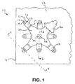
- resistor network assembly 10 has a planar substrate 11 having a top surface 12 and a bottom surface 13.
- the substrate 11 is preferably made out of a ceramic material such as alumina oxide.
- Resistors 14 are disposed and trimmed on the top surface 12 by conventional thick film resistor processing techniques. Resistors 14 have a first end 15 and a second end 17.
- Top conductors 16 are disposed on the top surface 12 and bottom conductors 21 are disposed on the bottom surface 13 by conventional thick film conductor processing techniques.
- Conductors 16 are electrically connected to the first end 15 of resistors 14.
- the conductors 16 and resistors 14 slightly overlap and sinter to form a mechanical and electrical bond during processing.
- a top common conductor 20 is located on top surface 12 and is electrically connected to the second resistor end 17.
- a bottom conductor 23 is located on bottom surface 13.
- the ceramic substrate 11 has cylindrical vias 18 formed therein and which extend through the substrate 11 and are filled with a conductive via fill 19.
- a cylindrical common via 22 extends through the substrate 11 and is filled with a common conductive via fill 24.
- the via fill material is a conventional thick film conductor that is screened into the vias and fired.
- the via fill 19 electrically connects the top and bottom conductors 16 and 21.
- the common via fill 24 electrically connects the top and bottom common conductors 20 and 23.
- Solder spheres 28 are mechanically and electrically attached to the bottom conductors 21 and 23.
- the solder spheres are 10% tin and 90% lead and are commercially available from Alpha Metals Corporation.
- the solder spheres 28 are attached to the conductors 21 and 23 by a reflowed solder paste 29.
- the reflowed solder paste is 63% lead and 37% tin which has a low melting point.
- a terminating voltage is applied to the common via 22 through sphere 28 where the sphere 28 connects to an external electrical circuit such as on a printed circuit board.
- a cover coat 26 is placed over the resistors, the conductors and the common conductor to protect the resistor network from corrosion and abrasion.
- the top common conductor 20 has a star shape and the common via 22 is generally located near the center of the star shape.
- the top common conductor 23 star shape provides a short common connection to the terminating voltage which is connected to the solder sphere 28 through via 22 and minimizes inductance of the common conductor 23 which minimizes cross-talk noise between the resistor/conductor pairs.
- Figure 3 shows a perspective cross-sectional view of figure 1 along line 3-3 with the cover coat 26 removed.
- Figure 4 shows an electrical schematic of the resistor network assembly 10.
- the resistors 14 are connected through terminals 30 to the individual signal lines that are desired to be terminated.
- the common terminal 32 is connected to a terminating voltage of magnitude +V.
- the resistor 14 value is chosen to match the impedance value of the signal line being terminated.
- Resistor network assembly 10 is assembled by the following process sequence:
- resistors there are many different ways of accomplishing the preferred embodiment. For example, although it is contemplated to make substrate 14 out of ceramic, other suitable materials would work, like polyamide or FR4. These materials would require a different resistor system. Additionally, although only one group of 8 resistors 14 was shown on substrate 11, more or fewer resistors 14 could be tied to common via 22. More than one group of resistor network 10 can be placed on one substrate 11.
- the common conductor 20 has shown the common conductor 20 as having a star shape, other star shapes are contemplated such as a star with anywhere from 2 to 100 points.
- the specification showed the common via 22 located near the center of the star shape. It is contemplated to place the common via 22 at other locations such as near the edge of the common conductor 20.
- the specification has shown the resistor network assembly 10 with a cover coat 26. It is contemplated, however, to omit the cover coat.
- solder preforms in place of solder spheres 28.
- solder donuts or wire or squares could be used.
- the solder could be made from materials other than 10/90 tin lead.
- a mixture of tin/indium or tin/bismuth could be used if a lower melting solder is desired.
- a mixture of tin/silver or tin/antimony could be used if a higher temperature solder is desired.
- the steps of processing sequence could be modified from that shown in the specification to produce the same end result.
- the resistors 14 could be placed before the conductors 16 and 20 or the screening of the bottom conductors 21 and 23 could be omitted and the solder spheres 28 reflow soldered directly to the via fill materials 19 and 24.
Description
- This invention generally relates to resistors for electronics. Specifically, the invention is a group of impedance matching or terminating resistors mounted in a high density network or array package using spherical solder connections and having low noise characteristics.
- Resistor networks are commonly used to terminate high speed digital signal lines to minimize unwanted reflections back through the transmission structure which is typically a printed circuit board. In most applications, the terminations are made by placing a resistor with a resistance matching the impedance of the transmission line, at the end of the transmission line. One end of the resistor is connected to a common termination voltage and the other end is connected to the signal line. For these applications a bussed resistor network is a convenient solution, since one end of the termination is common to all signal lines.
- The previous resistor network designs including surface mount, SIP and DIP versions have had resistors and conductor arrangements with individual conductor lines running for a length of same distance on the network before being tied to a common point. This is necessitated because all the external off resistor network connections are made at the periphery of the device and a conductor must be run from the periphery of the device to the individual resistor. The lengthy line length causes each resistor/conductor pair to have a higher mutual inductance between adjoining resistor/conductor pairs and leads to significant cross-talk noise being coupled between the resistor/conductor pairs when the resistor network is employed in its typical use as a terminating or impedance matching resistor for simultaneously switching transistors in an electronic device. As the transistor density and speed of semiconductor devices increase, the problem of cross-talk noise causing an erroneous signal becomes more of a problem in all areas of the electronic package and must be taken into consideration when designing electronic packaging. Further, at high frequencies, the high inductance of the common termination lines can cause a high impedance to appear at the end of the transmission line.
- Despite the advantages of each type of prior art resistor network, none have been easily or economically manufactured with a high density of interconnects per unit area on a printed circuit board. In particular, providing the electrical connections only on the periphery of the resistor network causes the electrical leads to be tightly spaced on the edge of the device, while the area in the interior of the device is unused for electrical interconnections.
- Therefore, there is a current unmet and heretofore long felt need for a resistor network with higher density, low cross-talk noise and improved signal integrity.
- Examples of patents related to the present invention are as follows, and each patent is herein incorporated by reference for the supporting teachings;
- U.S. patent no.4,945,399, is an electronic package with integrated distributed decoupling capacitors.
- U.S. patent no.5,557,502, is a ball grid array package.
- U.S. patent no.4,300,115, is a multi-layer via resistor.
- U.S. patent no.4,658,234, is a resistor network.
- U.S. patent no.5,821,619, is an all ceramic surface mount sip and dip network having spacers and solder barriers.
- U.S. patent no. 5,379,190, is a chip type composite electronic part and manufacturing method.
- U.S. patent no.4,332,341, is a fabrication of circuit packages using solid phase solder bonding.
- U.S. patent no.5,539,186, is a temperature controlled multi-layer module.
- U.S. patent no.5,216,404, is a SIC thin film thermistor.
- U.S. patent no.4,654,628, is a network resistor unit.
- U.S. patent no.5,661,450, is a low inductance termination resistor array comprising circular resistors, each with a central via at its centre and a plurality of vias connected through a common conductor to the circumferences of all the resistors.
- U.S. patent no.5,729,438, is a pad array for eg resistors, where the respective ends of all the resistors are connected to one or other of two respective common vias.
- It is a feature of the invention to provide a resistor network for terminating active electronic devices that has low cross-talk noise between the adjoining resistors and the conductors that connect the resistors to other electronic packages. Specifically, there is a substrate, several resistors, conductors, and vias arranged in a configuration to minimize cross-talk noise. Solder spheres are used to connect the resistors to other electronic circuitry such as a printed circuit board.
- It is a feature of the invention to provide a low cross-talk resistor network according to claim 1. The network comprises a substrate having a first surface and a second surface. A plurality of resistors are disposed on the first surface, each resistor having a first end and a second end. A common via extends through the substrate. A plurality of first vias extend through the substrate, connected to the first end of each resistor. A common conductor is connected between the common via and the second end of each resistor, the common conductor having a star shape. A plurality of solder spheres are located on the second surface, connected to the common via and the first vias. The network is characterised in that one of said plurality of resistors is disposed at each point of the star shape of the common conductor.
- It is a feature of the invention to provide a cover coat disposed over the conductors and resistors.
- It is a feature of the invention to provide the common conductor with a star shape which minimizes inductance of the common conductor.
- It is a feature of the invention to provide a common via located near the center of the star shape.
- It is a further feature of the invention to provide a method of making the resistor network according to
claim 3 as defined in the preceding paragraphs. - There has thus been outlined, rather broadly, the more important features of the invention so that the detailed description thereof that follows may be better understood, and so that the present contribution to the art may be better appreciated. There are, of course, additional features of the invention that will be described hereinafter and which will form the subject matter of the appended claims. Those skilled in the art will appreciate that the preferred embodiment may readily be used as a basis for the designing of other structures, methods and systems for carrying out the several purposes of the present invention falling within the scope of the appended claims.
-
- FIG. 1 is a partial top view of the low cross-talk ball grid array resistor network with a portion of the cover coat removed.
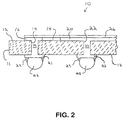
- FIG. 2 is a cross-sectional view of figure 1 along line 2-2.
- FIG. 3 is a perspective cross-sectional view of figure 1 along line 3-3.
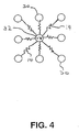
- FIG. 4 is an electrical schematic of the resistor network of figure 1.
- It is noted that the drawings of the invention are not to scale. The drawings are merely schematic representations, not intended to portray specific parameters of the invention. The drawings are intended to depict only typical embodiments of the invention, and therefore should not be considered as limiting the scope of the invention. The invention will be described with additional specificity and detail through the accompanying drawings. The description of the invention may contain, for example, such descriptive terms as up, down, top, bottom, right or left. These terms are meant to provide a general
- Referring to figures 1 and 2, there is a low cross-talk noise
resistor network assembly 10. In particular,resistor network assembly 10 has aplanar substrate 11 having atop surface 12 and abottom surface 13. Thesubstrate 11 is preferably made out of a ceramic material such as alumina oxide.Resistors 14 are disposed and trimmed on thetop surface 12 by conventional thick film resistor processing techniques.Resistors 14 have a first end 15 and a second end 17.Top conductors 16 are disposed on thetop surface 12 andbottom conductors 21 are disposed on thebottom surface 13 by conventional thick film conductor processing techniques.Conductors 16 are electrically connected to the first end 15 ofresistors 14. Theconductors 16 andresistors 14 slightly overlap and sinter to form a mechanical and electrical bond during processing. - A top
common conductor 20 is located ontop surface 12 and is electrically connected to the second resistor end 17. Abottom conductor 23 is located onbottom surface 13. Theceramic substrate 11 has cylindrical vias 18 formed therein and which extend through thesubstrate 11 and are filled with a conductive via fill 19. Similarly, a cylindrical common via 22 extends through thesubstrate 11 and is filled with a common conductive via fill 24. The via fill material is a conventional thick film conductor that is screened into the vias and fired. The via fill 19 electrically connects the top andbottom conductors common conductors Solder spheres 28 are mechanically and electrically attached to thebottom conductors solder spheres 28 are attached to theconductors solder paste 29. The reflowed solder paste is 63% lead and 37% tin which has a low melting point. A terminating voltage is applied to the common via 22 throughsphere 28 where thesphere 28 connects to an external electrical circuit such as on a printed circuit board. Acover coat 26 is placed over the resistors, the conductors and the common conductor to protect the resistor network from corrosion and abrasion. - The top
common conductor 20 has a star shape and the common via 22 is generally located near the center of the star shape. The topcommon conductor 23 star shape provides a short common connection to the terminating voltage which is connected to thesolder sphere 28 through via 22 and minimizes inductance of thecommon conductor 23 which minimizes cross-talk noise between the resistor/conductor pairs. - Figure 3 shows a perspective cross-sectional view of figure 1 along line 3-3 with the
cover coat 26 removed. - Figure 4 shows an electrical schematic of the
resistor network assembly 10. Theresistors 14 are connected throughterminals 30 to the individual signal lines that are desired to be terminated. The common terminal 32 is connected to a terminating voltage of magnitude +V. Theresistor 14 value is chosen to match the impedance value of the signal line being terminated. -
Resistor network assembly 10 is assembled by the following process sequence: - 1. Screen via fill 19 and 24 into
vias 18 and 22 ofsubstrate 11. - 2. Fire in oven.
- 3.
Screen conductors top surface 12. - 4. Fire in oven.
- 5.
Screen conductors bottom surface 13. - 6. Fire in oven.
- 7.
Screen resistors 14 ontotop surface 12. - 8. Fire in oven.
- 9.
Laser trim resistors 14 to proper resistance value. - 10. Screen and cure
cover coat 26. - 11.
Screen solder paste 29 ontoconductors - 12.
Place solder spheres 28 ontoconductors - 13.
Reflow solder paste 29 tobond spheres 28 toconductors - 14.
Test assembly 10. - One of ordinary skill in the art of making resistors will realize that there are many different ways of accomplishing the preferred embodiment. For example, although it is contemplated to make
substrate 14 out of ceramic, other suitable materials would work, like polyamide or FR4. These materials would require a different resistor system. Additionally, although only one group of 8resistors 14 was shown onsubstrate 11, more orfewer resistors 14 could be tied to common via 22. More than one group ofresistor network 10 can be placed on onesubstrate 11. - It is further possible to have other electrical connections through the substrate other than conductor filled vias. It is possible to use staked copper or metal pins in place of the via fill 19 and 24.
- Even though the specification has shown the
common conductor 20 as having a star shape, other star shapes are contemplated such as a star with anywhere from 2 to 100 points. The specification showed the common via 22 located near the center of the star shape. It is contemplated to place the common via 22 at other locations such as near the edge of thecommon conductor 20. - The specification has shown the
resistor network assembly 10 with acover coat 26. It is contemplated, however, to omit the cover coat. - Another variation of the preferred embodiment is to use other types of solder preforms in place of
solder spheres 28. For example, solder donuts or wire or squares could be used. Further, the solder could be made from materials other than 10/90 tin lead. For example, a mixture of tin/indium or tin/bismuth could be used if a lower melting solder is desired. A mixture of tin/silver or tin/antimony could be used if a higher temperature solder is desired. - Further, the steps of processing sequence could be modified from that shown in the specification to produce the same end result. For example, the
resistors 14 could be placed before theconductors bottom conductors solder spheres 28 reflow soldered directly to the via fill materials 19 and 24. - While the invention has been taught with specific reference to these embodiments, someone skilled in the art will recognize that changes can be made in form and detail without departing from the scope of the invention as defined by the appended claims. The described embodiments are to be considered in all respects only as illustrative and not restrictive.
Claims (4)
- A low cross-talk resistor network, comprising:a) a substrate (11) having a first surface (12) and second surface (13);b) a plurality of resistors (14), disposed on the first surface (12), each resistor having a first end (15) and a second end (17);c) a common via (22), extending through the substrate (11);d) a plurality of first vias (18), extending through the substrate (11), connected to the first end (15) of each resistor;e) a common conductor (20) connected between the common via (22) and the second end (17) of each resistor (14); said common conductor (20) having a star shape; andf) a plurality of solder spheres (28), located on the second surface (13), connected to the common via (22) and the first vias (18);characterised in that one of said plurality of resistors is disposed at each point of the star shape of the common conductor (20).
- The resistor network according to Claim 1, wherein a cover coat (26) is disposed over the first surface (12).
- A method of forming a low cross-talk resistor network, comprising the steps of:a) providing a substrate (11) having a first surface (12) and a second surface (13);b) providing a common via (22), extending between the first surface (12) and the second surface (13);c) providing a plurality of first vias (18), extending between the first surface (12) and the second surface (13);d) forming a common conductor (20), disposed on the first surface (12) and connected to the common via (22), the common conductor (20) having a star shape;e) forming a plurality of resistors (14) on the first surface (12), each resistor (14) having a first end (15) connected to the first vias (18) and a second end (17) connected to the common via (22); andf) disposing a plurality of solder spheres (28) on the second surface (13), each solder sphere (28) connected to the common via (22) or the first vias (18);the method characterised in that the step of forming the plurality of resistors on the first surface comprises forming said resistors so that one of said plurality of resistors is disposed at each point of the star shape of the common conductor (20).
- The method according to Claim 3, further comprising disposing a cover coat (26) over the resistors (14), the common conductor (20), the first vias (18) and the common via (22).
Applications Claiming Priority (2)
| Application Number | Priority Date | Filing Date | Title |
|---|---|---|---|
| US132081 | 1993-10-05 | ||
| US09/132,081 US5977863A (en) | 1998-08-10 | 1998-08-10 | Low cross talk ball grid array resistor network |
Publications (3)
| Publication Number | Publication Date |
|---|---|
| EP0980079A2 EP0980079A2 (en) | 2000-02-16 |
| EP0980079A3 EP0980079A3 (en) | 2002-01-02 |
| EP0980079B1 true EP0980079B1 (en) | 2007-02-07 |
Family
ID=22452375
Family Applications (1)
| Application Number | Title | Priority Date | Filing Date |
|---|---|---|---|
| EP99306022A Expired - Lifetime EP0980079B1 (en) | 1998-08-10 | 1999-07-29 | Low cross-talk ball grid array resistor network |
Country Status (6)
| Country | Link |
|---|---|
| US (1) | US5977863A (en) |
| EP (1) | EP0980079B1 (en) |
| JP (1) | JP2000124015A (en) |
| KR (1) | KR100612773B1 (en) |
| DE (1) | DE69935051T2 (en) |
| TW (1) | TW432398B (en) |
Families Citing this family (21)
| Publication number | Priority date | Publication date | Assignee | Title |
|---|---|---|---|---|
| US6326677B1 (en) | 1998-09-04 | 2001-12-04 | Cts Corporation | Ball grid array resistor network |
| US6194979B1 (en) * | 1999-03-18 | 2001-02-27 | Cts Corporation | Ball grid array R-C network with high density |
| US6246312B1 (en) | 2000-07-20 | 2001-06-12 | Cts Corporation | Ball grid array resistor terminator network |
| US6576489B2 (en) * | 2001-05-07 | 2003-06-10 | Applied Materials, Inc. | Methods of forming microstructure devices |
| US6577225B1 (en) | 2002-04-30 | 2003-06-10 | Cts Corporation | Array resistor network |
| JP5091406B2 (en) * | 2002-11-21 | 2012-12-05 | ハドコ サンタ クララ,インコーポレイテッド | Laser trimming of resistors |
| US6972391B2 (en) * | 2002-11-21 | 2005-12-06 | Hadco Santa Clara, Inc. | Laser trimming of annular passive components |
| US7297896B2 (en) * | 2002-11-21 | 2007-11-20 | Hadco Santa Clara, Inc. | Laser trimming of resistors |
| US6897761B2 (en) * | 2002-12-04 | 2005-05-24 | Cts Corporation | Ball grid array resistor network |
| US6882266B2 (en) * | 2003-01-07 | 2005-04-19 | Cts Corporation | Ball grid array resistor network having a ground plane |
| US7180186B2 (en) * | 2003-07-31 | 2007-02-20 | Cts Corporation | Ball grid array package |
| US6946733B2 (en) * | 2003-08-13 | 2005-09-20 | Cts Corporation | Ball grid array package having testing capability after mounting |
| US20050062587A1 (en) * | 2003-09-24 | 2005-03-24 | Wei-Chun Yang | Method and structure of a substrate with built-in via hole resistors |
| US7342804B2 (en) * | 2004-08-09 | 2008-03-11 | Cts Corporation | Ball grid array resistor capacitor network |
| US7724109B2 (en) * | 2005-11-17 | 2010-05-25 | Cts Corporation | Ball grid array filter |
| JP2007150201A (en) * | 2005-11-30 | 2007-06-14 | Toshiba Corp | Chip resistor |
| US7940148B2 (en) * | 2006-11-02 | 2011-05-10 | Cts Corporation | Ball grid array resonator |
| WO2008063507A2 (en) * | 2006-11-17 | 2008-05-29 | Cts Corporation | Voltage controlled oscillator module with ball grid array resonator |
| US20090236134A1 (en) * | 2008-03-20 | 2009-09-24 | Knecht Thomas A | Low frequency ball grid array resonator |
| KR20160052283A (en) * | 2014-11-04 | 2016-05-12 | 삼성전기주식회사 | Resistor element, manufacturing method of the same ans board having the same mounted thereon |
| KR101670140B1 (en) * | 2014-12-15 | 2016-10-27 | 삼성전기주식회사 | Resistor element, manufacturing method of the same ans board having the same mounted thereon |
Family Cites Families (13)
| Publication number | Priority date | Publication date | Assignee | Title |
|---|---|---|---|---|
| US4332341A (en) * | 1979-12-26 | 1982-06-01 | Bell Telephone Laboratories, Incorporated | Fabrication of circuit packages using solid phase solder bonding |
| US4300115A (en) * | 1980-06-02 | 1981-11-10 | The United States Of America As Represented By The Secretary Of The Army | Multilayer via resistors |
| US4658234A (en) * | 1984-06-06 | 1987-04-14 | Alps Electric Co., Ltd. | Resistor network |
| JPH0331046Y2 (en) * | 1985-03-01 | 1991-07-01 | ||
| US4945399A (en) * | 1986-09-30 | 1990-07-31 | International Business Machines Corporation | Electronic package with integrated distributed decoupling capacitors |
| DE69117374T2 (en) * | 1990-07-25 | 1996-08-01 | Matsushita Electric Ind Co Ltd | SiC thin film thermistor and method and manufacturing process. |
| JP2637662B2 (en) * | 1992-02-25 | 1997-08-06 | ローム株式会社 | Method of manufacturing chip-type composite electronic component and method of manufacturing chip-type network resistor |
| US5539186A (en) * | 1992-12-09 | 1996-07-23 | International Business Machines Corporation | Temperature controlled multi-layer module |
| KR0130030B1 (en) * | 1994-08-25 | 1998-10-01 | 김광호 | Column redundancy circuit and method for semiconductor memory device |
| US5557502A (en) * | 1995-03-02 | 1996-09-17 | Intel Corporation | Structure of a thermally and electrically enhanced plastic ball grid array package |
| US5661450A (en) * | 1995-11-21 | 1997-08-26 | Sun Microsystems, Inc. | Low inductance termination resistor arrays |
| WO1997030461A1 (en) * | 1996-02-15 | 1997-08-21 | Bourns, Inc. | Resistor network in ball grid array package |
| US5729438A (en) * | 1996-06-07 | 1998-03-17 | Motorola, Inc. | Discrete component pad array carrier |
-
1998
- 1998-08-10 US US09/132,081 patent/US5977863A/en not_active Expired - Lifetime
-
1999
- 1999-07-29 EP EP99306022A patent/EP0980079B1/en not_active Expired - Lifetime
- 1999-07-29 DE DE69935051T patent/DE69935051T2/en not_active Expired - Fee Related
- 1999-07-29 KR KR1019990031023A patent/KR100612773B1/en not_active IP Right Cessation
- 1999-07-31 TW TW088113090A patent/TW432398B/en not_active IP Right Cessation
- 1999-08-05 JP JP11222727A patent/JP2000124015A/en active Pending
Also Published As
| Publication number | Publication date |
|---|---|
| EP0980079A3 (en) | 2002-01-02 |
| JP2000124015A (en) | 2000-04-28 |
| DE69935051T2 (en) | 2007-11-15 |
| EP0980079A2 (en) | 2000-02-16 |
| KR20000016980A (en) | 2000-03-25 |
| TW432398B (en) | 2001-05-01 |
| DE69935051D1 (en) | 2007-03-22 |
| KR100612773B1 (en) | 2006-08-18 |
| US5977863A (en) | 1999-11-02 |
Similar Documents
| Publication | Publication Date | Title |
|---|---|---|
| EP0980079B1 (en) | Low cross-talk ball grid array resistor network | |
| US6005777A (en) | Ball grid array capacitor | |
| US6326677B1 (en) | Ball grid array resistor network | |
| US6108212A (en) | Surface-mount device package having an integral passive component | |
| KR100367045B1 (en) | Mechanisms with inner layers that support surface-mount components | |
| JP3898891B2 (en) | Via plug adapter | |
| US6246312B1 (en) | Ball grid array resistor terminator network | |
| US6256877B1 (en) | Method for transforming a substrate with edge contacts into a ball grid array | |
| US7335995B2 (en) | Microelectronic assembly having array including passive elements and interconnects | |
| EP0423821B1 (en) | Surface-mount network device | |
| US9095067B2 (en) | Apparatus and method for vertically-structured passive components | |
| US5953213A (en) | Multichip module | |
| US6344682B1 (en) | Semiconductor device comprising a semiconductor element mounted on a substrate and covered by a wiring board | |
| JP2004534376A (en) | Multi-stage array capacitor and manufacturing method thereof | |
| US6097277A (en) | Resistor network with solder sphere connector | |
| US20080043447A1 (en) | Semiconductor package having laser-embedded terminals | |
| US20040120127A1 (en) | Compact circuit module having high mounting accuracy and method of manufacturing the same | |
| US6310392B1 (en) | Stacked micro ball grid array packages | |
| US5384433A (en) | Printed circuit structure including power, decoupling and signal termination | |
| US6577225B1 (en) | Array resistor network | |
| US7084501B2 (en) | Interconnecting component | |
| US8324727B2 (en) | Low profile discrete electronic components and applications of same | |
| US5990421A (en) | Built in board resistors | |
| WO1997030461A1 (en) | Resistor network in ball grid array package | |
| KR920005952Y1 (en) | Semiconductor apparatus |
Legal Events
| Date | Code | Title | Description |
|---|---|---|---|
| PUAI | Public reference made under article 153(3) epc to a published international application that has entered the european phase |
Free format text: ORIGINAL CODE: 0009012 |
|
| AK | Designated contracting states |
Kind code of ref document: A2 Designated state(s): AT BE CH CY DE DK ES FI FR GB GR IE IT LI LU MC NL PT SE Kind code of ref document: A2 Designated state(s): DE FR GB |
|
| AX | Request for extension of the european patent |
Free format text: AL;LT;LV;MK;RO;SI |
|
| PUAL | Search report despatched |
Free format text: ORIGINAL CODE: 0009013 |
|
| AK | Designated contracting states |
Kind code of ref document: A3 Designated state(s): AT BE CH CY DE DK ES FI FR GB GR IE IT LI LU MC NL PT SE |
|
| AX | Request for extension of the european patent |
Free format text: AL;LT;LV;MK;RO;SI |
|
| 17P | Request for examination filed |
Effective date: 20020629 |
|
| AKX | Designation fees paid |
Free format text: DE FR GB |
|
| 17Q | First examination report despatched |
Effective date: 20050208 |
|
| GRAP | Despatch of communication of intention to grant a patent |
Free format text: ORIGINAL CODE: EPIDOSNIGR1 |
|
| GRAS | Grant fee paid |
Free format text: ORIGINAL CODE: EPIDOSNIGR3 |
|
| GRAA | (expected) grant |
Free format text: ORIGINAL CODE: 0009210 |
|
| AK | Designated contracting states |
Kind code of ref document: B1 Designated state(s): DE FR GB |
|
| REG | Reference to a national code |
Ref country code: GB Ref legal event code: FG4D |
|
| REF | Corresponds to: |
Ref document number: 69935051 Country of ref document: DE Date of ref document: 20070322 Kind code of ref document: P |
|
| ET | Fr: translation filed | ||
| PLBE | No opposition filed within time limit |
Free format text: ORIGINAL CODE: 0009261 |
|
| STAA | Information on the status of an ep patent application or granted ep patent |
Free format text: STATUS: NO OPPOSITION FILED WITHIN TIME LIMIT |
|
| 26N | No opposition filed |
Effective date: 20071108 |
|
| PGFP | Annual fee paid to national office [announced via postgrant information from national office to epo] |
Ref country code: FR Payment date: 20090717 Year of fee payment: 11 |
|
| PGFP | Annual fee paid to national office [announced via postgrant information from national office to epo] |
Ref country code: GB Payment date: 20090727 Year of fee payment: 11 Ref country code: DE Payment date: 20090729 Year of fee payment: 11 |
|
| GBPC | Gb: european patent ceased through non-payment of renewal fee |
Effective date: 20100729 |
|
| REG | Reference to a national code |
Ref country code: FR Ref legal event code: ST Effective date: 20110331 |
|
| PG25 | Lapsed in a contracting state [announced via postgrant information from national office to epo] |
Ref country code: DE Free format text: LAPSE BECAUSE OF NON-PAYMENT OF DUE FEES Effective date: 20110201 |
|
| REG | Reference to a national code |
Ref country code: DE Ref legal event code: R119 Ref document number: 69935051 Country of ref document: DE Effective date: 20110201 |
|
| PG25 | Lapsed in a contracting state [announced via postgrant information from national office to epo] |
Ref country code: FR Free format text: LAPSE BECAUSE OF NON-PAYMENT OF DUE FEES Effective date: 20100802 |
|
| PG25 | Lapsed in a contracting state [announced via postgrant information from national office to epo] |
Ref country code: GB Free format text: LAPSE BECAUSE OF NON-PAYMENT OF DUE FEES Effective date: 20100729 |