EP0978143B1 - Semiconductor device comprising a half-bridge circuit - Google Patents
Semiconductor device comprising a half-bridge circuit Download PDFInfo
- Publication number
- EP0978143B1 EP0978143B1 EP98945481A EP98945481A EP0978143B1 EP 0978143 B1 EP0978143 B1 EP 0978143B1 EP 98945481 A EP98945481 A EP 98945481A EP 98945481 A EP98945481 A EP 98945481A EP 0978143 B1 EP0978143 B1 EP 0978143B1
- Authority
- EP
- European Patent Office
- Prior art keywords
- type
- zone
- cup
- shaped
- transistor
- Prior art date
- Legal status (The legal status is an assumption and is not a legal conclusion. Google has not performed a legal analysis and makes no representation as to the accuracy of the status listed.)
- Expired - Lifetime
Links
- 239000004065 semiconductor Substances 0.000 title claims abstract description 18
- 239000000758 substrate Substances 0.000 claims abstract description 32
- 230000015556 catabolic process Effects 0.000 description 5
- 230000001939 inductive effect Effects 0.000 description 4
- 230000000694 effects Effects 0.000 description 3
- 238000010586 diagram Methods 0.000 description 2
- 238000009792 diffusion process Methods 0.000 description 2
- 230000005684 electric field Effects 0.000 description 2
- 230000003071 parasitic effect Effects 0.000 description 2
- XUIMIQQOPSSXEZ-UHFFFAOYSA-N Silicon Chemical compound [Si] XUIMIQQOPSSXEZ-UHFFFAOYSA-N 0.000 description 1
- 230000001427 coherent effect Effects 0.000 description 1
- 238000010276 construction Methods 0.000 description 1
- 230000009849 deactivation Effects 0.000 description 1
- 239000002184 metal Substances 0.000 description 1
- 238000000034 method Methods 0.000 description 1
- 229910021420 polycrystalline silicon Inorganic materials 0.000 description 1
- 229910052710 silicon Inorganic materials 0.000 description 1
- 239000010703 silicon Substances 0.000 description 1
- 238000004804 winding Methods 0.000 description 1
Images

Classifications
-
- H—ELECTRICITY
- H10—SEMICONDUCTOR DEVICES; ELECTRIC SOLID-STATE DEVICES NOT OTHERWISE PROVIDED FOR
- H10D—INORGANIC ELECTRIC SEMICONDUCTOR DEVICES
- H10D84/00—Integrated devices formed in or on semiconductor substrates that comprise only semiconducting layers, e.g. on Si wafers or on GaAs-on-Si wafers
-
- H—ELECTRICITY
- H10—SEMICONDUCTOR DEVICES; ELECTRIC SOLID-STATE DEVICES NOT OTHERWISE PROVIDED FOR
- H10D—INORGANIC ELECTRIC SEMICONDUCTOR DEVICES
- H10D30/00—Field-effect transistors [FET]
- H10D30/60—Insulated-gate field-effect transistors [IGFET]
- H10D30/64—Double-diffused metal-oxide semiconductor [DMOS] FETs
- H10D30/65—Lateral DMOS [LDMOS] FETs
-
- H—ELECTRICITY
- H10—SEMICONDUCTOR DEVICES; ELECTRIC SOLID-STATE DEVICES NOT OTHERWISE PROVIDED FOR
- H10D—INORGANIC ELECTRIC SEMICONDUCTOR DEVICES
- H10D84/00—Integrated devices formed in or on semiconductor substrates that comprise only semiconducting layers, e.g. on Si wafers or on GaAs-on-Si wafers
- H10D84/80—Integrated devices formed in or on semiconductor substrates that comprise only semiconducting layers, e.g. on Si wafers or on GaAs-on-Si wafers characterised by the integration of at least one component covered by groups H10D12/00 or H10D30/00, e.g. integration of IGFETs
- H10D84/811—Combinations of field-effect devices and one or more diodes, capacitors or resistors
-
- H—ELECTRICITY
- H10—SEMICONDUCTOR DEVICES; ELECTRIC SOLID-STATE DEVICES NOT OTHERWISE PROVIDED FOR
- H10D—INORGANIC ELECTRIC SEMICONDUCTOR DEVICES
- H10D84/00—Integrated devices formed in or on semiconductor substrates that comprise only semiconducting layers, e.g. on Si wafers or on GaAs-on-Si wafers
- H10D84/80—Integrated devices formed in or on semiconductor substrates that comprise only semiconducting layers, e.g. on Si wafers or on GaAs-on-Si wafers characterised by the integration of at least one component covered by groups H10D12/00 or H10D30/00, e.g. integration of IGFETs
- H10D84/82—Integrated devices formed in or on semiconductor substrates that comprise only semiconducting layers, e.g. on Si wafers or on GaAs-on-Si wafers characterised by the integration of at least one component covered by groups H10D12/00 or H10D30/00, e.g. integration of IGFETs of only field-effect components
- H10D84/83—Integrated devices formed in or on semiconductor substrates that comprise only semiconducting layers, e.g. on Si wafers or on GaAs-on-Si wafers characterised by the integration of at least one component covered by groups H10D12/00 or H10D30/00, e.g. integration of IGFETs of only field-effect components of only insulated-gate FETs [IGFET]
Definitions
- the invention relates to a semiconductor device comprising a half-bridge circuit with two n-channel DMOS transistors forming a series connection between a terminal V ss for a low voltage and a terminal V dd for a high voltage, which semiconductor device also comprises a semiconductor body with a p-type substrate and, provided on said substrate, an epitaxial layer in which, for the transistors, two separate regions are defined which are surrounded within the semiconductor body by two electrically insulated cup-shaped n-type zones which each have a bottom formed by a buried n-type zone at the interface between the substrate and the epitaxial layer, and a raised wall formed by an n-type zone which extends from the surface across the thickness of the epitaxial layer to the underlying buried zone, each of the transistors comprising an n-type source and drain zone, the source zone of each transistor being located in a p-type backgate region, and, of one of the transistors, hereinafter referred to as first transistor, the source zone being connected to V
- Such a device which can be used, for example, in an electronic ballast for gas-discharge lamps or in driver circuits for motors is known, inter alia, from the article " A versatile 250/300-V IC process for analog and switching applications" A.W. Ludikhuize, published in IEEE Transactions on Electron Devices, Vol. ED-33, No. 12, December 1986, pp. 2008/2015 .
- the use of two half bridges enables the circuit to be readily extended to a full bridge circuit.
- the use of DMOS transistors has various advantages which are known per se, such as sturdiness, which makes the transistor resistant to high voltages and/or high powers.
- this type of transistor can very suitably be used in the case of inductive loads as a result of which the voltage at the output may be higher than V dd and lower than V ss , as the electric charge can be efficiently removed via the body diode of the DMOS.
- an n-type epitaxial layer is used in which islands are formed in known manner by means of a deep p-type diffusion, which islands accommodate the transistors; see, in particular, Fig. 14 and Fig. 15 of said publication.
- the half bridge is constructed symmetrically, that is, the construction of the transistors is identical.
- the n-type cup-shaped zone is connected, both in the first transistor (also referred to as low-side transistor) and in the second transistor (also referred to as high-side transistor), to the drain. In the case of the high-side transistor, this will generally not be problematic.
- the drain, and hence the n-type cup-shaped zone is coupled to the output of the (half) bridge and thus its potential varies.
- the voltage at the output that is the node of the drain of the first transistor and the source of the second transistor, may be reduced to a level which is lower than the substrate voltage, so that the pn-junction between the substrate and the n-type cup-shaped zone of the first transistor becomes forward-poled and electrons are injected into the substrate. This may cause disturbances in other circuit elements or latch-up.
- dV/dt effects may occur, which, in the case of a rapid increase of the potential on the output, also cause a local increase of the potential in the, generally rather high-ohmic, substrate, so that one may observe the occurrence of disturbances and latch-up with neighboring n-type zones at, for example 0 V.
- the invention provides a device as defined by claim 1.
- the semiconductor device in accordance with the invention is characterized in that within the n-type cup-shaped zone belonging to the first transistor, a p-type cup-shaped zone is formed whose bottom is formed by a p-type buried zone which is isolated from the substrate by the buried n-type zone of the n-type cup-shaped zone, and the raised wall of said p-type cup-shaped zone being formed by a p-type zone which extends from the surface to the buried p-type zone, the n-type source and drain zones and a p-type backgate region of the first transistor being arranged in the region surrounded by the p-type cup-shaped zone, and the n-type and p-type cup-shaped zones both being connected to the source zone and the backgate region and to V ss , and the n-type source and drain zones and a p-type backgate region of the second transistor being arranged in the region which is defined by the second n-type cup-shaped zone and which is connected to V dd
- the p-type cup-shaped zone enables the n-type cup-shaped zone of the first transistor (low-side transistor) to be electrically insulated from the drain.
- the voltage V ss can be applied to the n-type cup-shaped zone, thereby precluding that the pn-junction between this zone and the substrate, to which substrate generally also a low voltage is applied, is forward biased when subjected to an inductive load.
- the above-described dV/dt effects are suppressed completely, or at least to a substantial degree, in that the n-type cup-shaped zone is at a fixed potential.
- the epitaxial layer may be of the n-type, with parts of the epitaxial layer being suitable for use as a drift region of the transistors.
- An embodiment which provenly offers particular advantages is characterized in that the epitaxial layer is of the p-type, in which, in each of the regions defined by the cup-shaped zones, an n-type zone, referred to as well, is formed, the well belonging to the first transistor being separated from the associated n-type cup-shaped zone by the p-type cup-shaped zone, and the n-type well belonging to the second transistor being conductively connected to the associated n-type cup-shaped zone.
- a preferred embodiment of a semiconductor device in accordance with the invention is characterized in that the overall doping level of the n-type well of the first transistor, in a direction transverse to the surface, is, at least locally, at most substantially equal to 3.10 12 atoms per cm 2 .
- this condition enables the n-type region to be depleted throughout its thickness before the occurrence of breakdown. Depletion causes the electric fields at the surface to be reduced such that the breakdown voltage becomes (substantially) equal to the theoretically maximum breakdown voltage.
- a further embodiment which, inter alia, has the advantage that also in the other transistor (i.e. high-side transistor), the resurf condition can be met, is characterized in that in the region defined by the n-type cup-shaped zone belonging to the second transistor, a p-type cup-shaped zone is arranged having a bottom formed by a buried p-type zone which is separated from the p-type substrate by the intermediate bottom of the n-type cup-shaped zone, and having a raised wall formed by a p-type region extending from the surface across the epitaxial layer to the buried p-type zone, the n-type source and drain zones and the p-type backgate region of the second transistor being formed in the region of the epitaxial layer surrounded by the cup-shaped p-type zone, and the source zone and the backgate region being jointly connected to the p-type cup-shaped zone.
- Fig. 1 shows a circuit diagram of a half-bridge circuit by means of which an alternating current can be sent through a load 1 with an inductance L, for example a motor winding.
- the current is supplied by a power supply having a terminal V dd for the high voltage and a terminal V ss for the low voltage.
- the bridge circuit comprises two n-channel transistors T 1 (low side) and T 2 (high side) of the DMOS type.
- the drain of the low-side transistor and the source of the high-side transistor are jointly connected to the output 4 of the bridge.
- the source of T 1 and the drain of T 2 are connected, respectively, to V ss and V dd .
- the DMOS transistors have an internal diode 3, also referred to as body diode, which is situated between the source and the drain, the anode of said diode being formed by the backgate region connected to the source, and the cathode of said diode being formed by the drain.
- the gate electrodes of the transistors are connected to a control circuit 5, only schematically shown in the drawing, which supplies control signals, so that the transistors are conducting and non-conducting substantially in phase-opposition,and the current can be carried, by the load 1, alternately in the one direction and the other direction.
- a terminal 2 of the load 1 can be connected to a point of a fixed potential, for example halfway V dd and V ss . At higher power values, it may be advantageous to connect said terminal 2 to the output of a similar half-bridge circuit, thus forming a full-bridge circuit.
- use can be made of three half bridges as shown in Fig. 1 .
- T 1 If, during operation, T 1 is conducting, electric current flows from terminal 2 to V ss .
- T 1 When T 1 is opened (non-conducting), current remains flowing at first due to the presence of the inductance L, so that the potential on the output 4 will increase and may even become higher than V dd .
- the bridge can be discharged again via the diode 3 of T 2 .
- deactivation of T 2 may cause the potential on the output 4 to decrease to a value below V ss , and the electric charge can be removed via the body diode 3 of T 1 .
- Fig. 2 is a sectional view of an embodiment of a semiconductor device in accordance with the invention.
- Said device comprises a p-type silicon substrate 10.
- the resistivity of the substrate is selected taking into account the maximum voltages it should be able to cope with, during operation, without the occurrence of breakdown, and amounts typically to, for example, 10 ⁇ .cm.
- the substrate 10 is epitaxially provided with a p-type layer 11 having a thickness, for example, of 5 ⁇ m and a resistivity of 10 ⁇ .cm. In the epitaxial layer 11, two separate regions are defined, i.e.
- the zones 12 and 13 are electrically separated from each other by intermediate parts of the p-type epitaxial layer 11 in which, if desired, highly doped p-type zones 14 may be provided.
- Said cup-shaped zones each comprise a bottom 12a, 13a which is provided as a highly doped buried n-type zone between the substrate and the epitaxial layer, while the raised walls of the cup-shaped zones are formed by highly doped zones 12b, 13b extending from the surface of the epitaxial layer to the buried zones and forming a coherent zone with said buried zones.
- the regions surrounded by the zones 12 and 13 are provided with relatively low-doped n-type zones 15 and 16, hereinafter referred to as well, which form drift regions of the DMOS transistors.
- Each n-type drift region comprises a p-type surface zone 17, 18, respectively, which forms a backgate region of the transistor.
- the source of the transistors comprises a highly-doped n-type surface zone 19, 20, respectively, which is arranged in the p-type backgate region.
- the surface of the epitaxial layer is covered with a dielectric layer 21 which, at the location of the channels of the transistors, changes into gate oxide on which the gate electrodes 22 and 23 are formed.
- the electrodes 22 and 23, which are customarily used to align the backgate regions 17, 18 and the source zones 19, 20 with respect to each other, are generally made of doped polycrystalline silicon (poly).
- a second, p-type cup-shaped zone 24 which isolates the n-type drift region 15 from the n-type cup-shaped zone 12.
- the bottom of the cup-shaped zone 24 is formed by a buried p-type layer; the raised wall 24b is formed by a p-type zone which extends from the surface to the buried layer 24b.
- the n-type cup-shaped zone and the p-type cup-shaped zone are both connected to the n-type source 19 and the backgate region 17.
- the p-type backgate region 17 and the p-type cup-shaped zone 24 border on each other and are connected, together with the n-type cup-shaped zone, to V ss via the metal source contact 25 which contacts these zones via windows in the oxide layer 21.
- the n-type cup-shaped zone forms the drain zone of T 2 and is connected via the connection 26 to V dd .
- the drain zone of T 1 is formed by the highly doped n-type zone 29 which is separated by the p-type zone 24 from the n-type zone 12 and the substrate 10.
- the drain zone 29 and the source zone 20 of T 2 are connected to the output terminal 4 via, respectively, the contacts 27 and 28.
- the charge is drained completely via the pn-junction between the p-type zones 17, 24 and the n-type zones 15, 29 (body diode 3 of transistor T 1 ). If the potential on the output terminal 4 becomes very high, that is higher than V dd , then, in the high-side transistor T 2 , the pn-junction between the backgate region 18 and the drain 13, 16 (body diode 3 of T 2 ) becomes forward-poled. In combination with the p-type substrate 10, these zones form a parasitic vertical pnp-transistor.
- the voltage between the emitter (p-type zone 18) and the collector (p-type substrate 10) is large, it is very important that the current passing through this parasitic transistor remains low so as to preclude that too much heat is generated. In the present example, this is achieved by the high doping level of the n-type zone 13 which forms part of the base of the transistor, so that substantially all of the charge is removed by the body diode 3 of the DMOS transistor.
- a further advantage of the device described herein can be achieved by selecting the doping level of the n-type drift region 15 of the low-side transistor to be such that the RESURF condition is met.
- the RESURF condition is described, inter alia, in the article " High Voltage, High Current Lateral Devices” by H. Vaes and J. Appels, published in Proc. IEDM 1980, pp. 87/90 .
- the meaning of this condition can be expressed as follows: the product of the thickness and the doping concentration of the n-type drift region 15 is, at least locally, (substantially) equal to 10 12 atoms per cm 2 .
- the n-type region 15 to be, at least locally, depleted from the buried p-type layer across its entire thickness, so that the electric fields at the surface are substantially reduced and electric breakdown occurs at a much higher voltage than in situations where this depletion is absent.
- the (average) doping concentration amounts to approximately 5.10 15 atoms per cm 3 .
- transistor T 1 is practically identical to T 1 of the preceding example.
- transistor T 2 comprises a cup-shaped p-type zone 30 which is situated within the region defined by the cup-shaped n-type zone 13.
- Said cup-shaped zone 30 comprises a buried p-type layer 30a, separated from the p-type substrate 10 by the buried n-type layer 13a, and a raised wall 30b which extends from the surface to the buried zone 30a in the epitaxial layer 11 and is separated from surrounding parts of the epitaxial layer by the n-type zone 13b.
- the transistors may be constructed substantially identically, with the backgate region 18 of T 2 bordering on the raised wall 30b of the cup-shaped p-type zone 30 which is short-circuited to the source zone 20 via the source contact 28.
- the drain comprises a highly doped n-type zone 31 which is provided with a drain contact 32.
- the n-type cup-shaped zone 13 includes a contact 33 which, together with the drain contact 32, is connected to V dd .
- the pn-junction between the cup-shaped zones 13 and 30 may become forward-poled.
- the holes injected into the zone 13 will be retarded by the highly doped n-type zone 13, thus precluding diffusion of these holes to the substrate 10.
- a suitable choice of the doping concentration of the drift region 16 of T 2 enables also the high-side transistor to be constructed as a RESURF transistor, in a manner similar to that of the low-side transistor T 1.
- an n-type epitaxial layer can be used instead of a p-type layer.
- the n-type drift regions in only a part, which borders on the highly-doped drain zones, of the regions surrounded by the cup-shaped zones, so that parts of the epitaxial layer around the backgate regions continue to be of the p-type. It is also possible to provide the transistors with a larger number of source regions forming an interdigital configuration with intermediate drain regions.
Landscapes
- Insulated Gate Type Field-Effect Transistor (AREA)
- Metal-Oxide And Bipolar Metal-Oxide Semiconductor Integrated Circuits (AREA)
Abstract
Description
- The invention relates to a semiconductor device comprising a half-bridge circuit with two n-channel DMOS transistors forming a series connection between a terminal Vss for a low voltage and a terminal Vdd for a high voltage, which semiconductor device also comprises a semiconductor body with a p-type substrate and, provided on said substrate, an epitaxial layer in which, for the transistors, two separate regions are defined which are surrounded within the semiconductor body by two electrically insulated cup-shaped n-type zones which each have a bottom formed by a buried n-type zone at the interface between the substrate and the epitaxial layer, and a raised wall formed by an n-type zone which extends from the surface across the thickness of the epitaxial layer to the underlying buried zone, each of the transistors comprising an n-type source and drain zone, the source zone of each transistor being located in a p-type backgate region, and, of one of the transistors, hereinafter referred to as first transistor, the source zone being connected to Vss and the drain zone being connected to the source zone of the second transistor whose drain zone is connected to Vdd. Such a device, which can be used, for example, in an electronic ballast for gas-discharge lamps or in driver circuits for motors is known, inter alia, from the article "A versatile 250/300-V IC process for analog and switching applications" A.W. Ludikhuize, published in IEEE Transactions on Electron Devices, Vol. ED-33, No. 12, December 1986, pp. 2008/2015. The use of two half bridges enables the circuit to be readily extended to a full bridge circuit. The use of DMOS transistors has various advantages which are known per se, such as sturdiness, which makes the transistor resistant to high voltages and/or high powers. In addition, this type of transistor can very suitably be used in the case of inductive loads as a result of which the voltage at the output may be higher than Vdd and lower than Vss, as the electric charge can be efficiently removed via the body diode of the DMOS.
- In the known device, an n-type epitaxial layer is used in which islands are formed in known manner by means of a deep p-type diffusion, which islands accommodate the transistors; see, in particular, Fig. 14 and Fig. 15 of said publication. The half bridge is constructed symmetrically, that is, the construction of the transistors is identical. As a result, the n-type cup-shaped zone is connected, both in the first transistor (also referred to as low-side transistor) and in the second transistor (also referred to as high-side transistor), to the drain. In the case of the high-side transistor, this will generally not be problematic. In the low-side transistor, however, the drain, and hence the n-type cup-shaped zone, is coupled to the output of the (half) bridge and thus its potential varies. In the case of an inductive load, the voltage at the output, that is the node of the drain of the first transistor and the source of the second transistor, may be reduced to a level which is lower than the substrate voltage, so that the pn-junction between the substrate and the n-type cup-shaped zone of the first transistor becomes forward-poled and electrons are injected into the substrate. This may cause disturbances in other circuit elements or latch-up. In addition, so-called dV/dt effects may occur, which, in the case of a rapid increase of the potential on the output, also cause a local increase of the potential in the, generally rather high-ohmic, substrate, so that one may observe the occurrence of disturbances and latch-up with neighboring n-type zones at, for example 0 V.
- It is an object of the invention to provide, inter alia, a half-bridge circuit comprising two series-connected n-channel DMOS transistors, in which these drawbacks are overcome or at least substantially reduced compared to the known device. The invention provides a device as defined by
claim 1. - The semiconductor device in accordance with the invention is characterized in that within the n-type cup-shaped zone belonging to the first transistor, a p-type cup-shaped zone is formed whose bottom is formed by a p-type buried zone which is isolated from the substrate by the buried n-type zone of the n-type cup-shaped zone, and the raised wall of said p-type cup-shaped zone being formed by a p-type zone which extends from the surface to the buried p-type zone, the n-type source and drain zones and a p-type backgate region of the first transistor being arranged in the region surrounded by the p-type cup-shaped zone, and the n-type and p-type cup-shaped zones both being connected to the source zone and the backgate region and to Vss, and the n-type source and drain zones and a p-type backgate region of the second transistor being arranged in the region which is defined by the second n-type cup-shaped zone and which is connected to Vdd. The p-type cup-shaped zone enables the n-type cup-shaped zone of the first transistor (low-side transistor) to be electrically insulated from the drain. By virtue thereof, the voltage Vss can be applied to the n-type cup-shaped zone, thereby precluding that the pn-junction between this zone and the substrate, to which substrate generally also a low voltage is applied, is forward biased when subjected to an inductive load. Moreover, the above-described dV/dt effects are suppressed completely, or at least to a substantial degree, in that the n-type cup-shaped zone is at a fixed potential.
- The epitaxial layer may be of the n-type, with parts of the epitaxial layer being suitable for use as a drift region of the transistors. An embodiment which provenly offers particular advantages is characterized in that the epitaxial layer is of the p-type, in which, in each of the regions defined by the cup-shaped zones, an n-type zone, referred to as well, is formed, the well belonging to the first transistor being separated from the associated n-type cup-shaped zone by the p-type cup-shaped zone, and the n-type well belonging to the second transistor being conductively connected to the associated n-type cup-shaped zone.
- Since the n-type cup-shaped zone no longer forms part of the drain of the low-side transistor, the n-type drift region within which the drain zone is formed can be given such a thickness and doping concentration that, in case the device must be operated at a high voltage, the resurf (reduced surface field) condition is met. Therefore, a preferred embodiment of a semiconductor device in accordance with the invention is characterized in that the overall doping level of the n-type well of the first transistor, in a direction transverse to the surface, is, at least locally, at most substantially equal to 3.1012 atoms per cm2. As is generally known, this condition enables the n-type region to be depleted throughout its thickness before the occurrence of breakdown. Depletion causes the electric fields at the surface to be reduced such that the breakdown voltage becomes (substantially) equal to the theoretically maximum breakdown voltage.
- A further embodiment which, inter alia, has the advantage that also in the other transistor (i.e. high-side transistor), the resurf condition can be met, is characterized in that in the region defined by the n-type cup-shaped zone belonging to the second transistor, a p-type cup-shaped zone is arranged having a bottom formed by a buried p-type zone which is separated from the p-type substrate by the intermediate bottom of the n-type cup-shaped zone, and having a raised wall formed by a p-type region extending from the surface across the epitaxial layer to the buried p-type zone, the n-type source and drain zones and the p-type backgate region of the second transistor being formed in the region of the epitaxial layer surrounded by the cup-shaped p-type zone, and the source zone and the backgate region being jointly connected to the p-type cup-shaped zone.
- These and other aspects of the invention will be apparent from and elucidated with reference to the embodiments described hereinafter.
- In the drawings:
-
Fig. 1 shows a circuit diagram of a half-bridge circuit with two n-channel DMOS transistors; -
Fig. 2 is a sectional view of a first embodiment of a semiconductor device comprising such a circuit in accordance with the invention; -
Fig. 3 is a sectional view of a variant of the embodiment in the preceding example. - It is noted that the sectional views shown in the drawing are schematic and not to scale.
-
Fig. 1 shows a circuit diagram of a half-bridge circuit by means of which an alternating current can be sent through aload 1 with an inductance L, for example a motor winding. The current is supplied by a power supply having a terminal Vdd for the high voltage and a terminal Vss for the low voltage. The bridge circuit comprises two n-channel transistors T1(low side) and T2 (high side) of the DMOS type. The drain of the low-side transistor and the source of the high-side transistor are jointly connected to theoutput 4 of the bridge. The source of T1 and the drain of T2 are connected, respectively, to Vss and Vdd. The DMOS transistors have an internal diode 3, also referred to as body diode, which is situated between the source and the drain, the anode of said diode being formed by the backgate region connected to the source, and the cathode of said diode being formed by the drain. The effect produced by this diode will be described hereinafter. The gate electrodes of the transistors are connected to acontrol circuit 5, only schematically shown in the drawing, which supplies control signals, so that the transistors are conducting and non-conducting substantially in phase-opposition,and the current can be carried, by theload 1, alternately in the one direction and the other direction. Aterminal 2 of theload 1 can be connected to a point of a fixed potential, for example halfway Vdd and Vss. At higher power values, it may be advantageous to connect saidterminal 2 to the output of a similar half-bridge circuit, thus forming a full-bridge circuit. For 3-phase applications, use can be made of three half bridges as shown inFig. 1 . - If, during operation, T1 is conducting, electric current flows from
terminal 2 to Vss. When T1 is opened (non-conducting), current remains flowing at first due to the presence of the inductance L, so that the potential on theoutput 4 will increase and may even become higher than Vdd. The bridge can be discharged again via the diode 3 of T2. Conversely, when T2 is conducting and the current flows from Vdd toterminal 2, deactivation of T2 may cause the potential on theoutput 4 to decrease to a value below Vss, and the electric charge can be removed via the body diode 3 of T1. -
Fig. 2 is a sectional view of an embodiment of a semiconductor device in accordance with the invention. Said device comprises a p-type silicon substrate 10. The resistivity of the substrate is selected taking into account the maximum voltages it should be able to cope with, during operation, without the occurrence of breakdown, and amounts typically to, for example, 10 Ω.cm. Thesubstrate 10 is epitaxially provided with a p-type layer 11 having a thickness, for example, of 5 µm and a resistivity of 10 Ω.cm. In theepitaxial layer 11, two separate regions are defined, i.e. a first region for T1, which is surrounded by the n-type cup-shaped zone 12, and a second region for T2, which is surrounded by the n-type cup-shaped zone 13. Thezones epitaxial layer 11 in which, if desired, highly doped p-type zones 14 may be provided. Said cup-shaped zones each comprise abottom doped zones zones type zones type surface zone type surface zone dielectric layer 21 which, at the location of the channels of the transistors, changes into gate oxide on which thegate electrodes electrodes backgate regions source zones - In accordance with the invention, in the region surrounded by the cup-shaped n-
type zone 12, a second, p-type cup-shaped zone 24 is provided which isolates the n-type drift region 15 from the n-type cup-shaped zone 12. The bottom of the cup-shaped zone 24 is formed by a buried p-type layer; the raisedwall 24b is formed by a p-type zone which extends from the surface to the buriedlayer 24b. The n-type cup-shaped zone and the p-type cup-shaped zone are both connected to the n-type source 19 and thebackgate region 17. In the present example, the p-type backgate region 17 and the p-type cup-shaped zone 24 border on each other and are connected, together with the n-type cup-shaped zone, to Vss via themetal source contact 25 which contacts these zones via windows in theoxide layer 21. On the other hand, at least in this example in which there is only one source zone, the n-type cup-shaped zone forms the drain zone of T2 and is connected via theconnection 26 to Vdd. The drain zone of T1 is formed by the highly doped n-type zone 29 which is separated by the p-type zone 24 from the n-type zone 12 and thesubstrate 10. Thedrain zone 29 and thesource zone 20 of T2 are connected to theoutput terminal 4 via, respectively, thecontacts - Since fixed voltages, i.e. Vss and Vdd, are applied to the n-type cup-shaped
zones substrate 1, which, in the known device, are caused by rapid and large voltage jumps at the output of the bridge circuit in combination with the relatively high resistivity of thesubstrate 11. As the n-type cup-shapedregion 12 which belongs to the low-side transistor T1 is connected to earth and not to thedrain 29 and theoutput 4, it is additionally precluded that the pn-junction between this zone and the p-type substrate becomes forward-poled when the output obtains a negative potential as a result of the inductive load. The charge is drained completely via the pn-junction between the p-type zones 17, 24 and the n-type zones 15, 29 (body diode 3 of transistor T1). If the potential on theoutput terminal 4 becomes very high, that is higher than Vdd, then, in the high-side transistor T2, the pn-junction between thebackgate region 18 and thedrain 13, 16 (body diode 3 of T2) becomes forward-poled. In combination with the p-type substrate 10, these zones form a parasitic vertical pnp-transistor. As the voltage between the emitter (p-type zone 18) and the collector (p-type substrate 10) is large, it is very important that the current passing through this parasitic transistor remains low so as to preclude that too much heat is generated. In the present example, this is achieved by the high doping level of the n-type zone 13 which forms part of the base of the transistor, so that substantially all of the charge is removed by the body diode 3 of the DMOS transistor. - A further advantage of the device described herein can be achieved by selecting the doping level of the n-
type drift region 15 of the low-side transistor to be such that the RESURF condition is met. The RESURF condition is described, inter alia, in the article "High Voltage, High Current Lateral Devices" by H. Vaes and J. Appels, published in Proc. IEDM 1980, pp. 87/90. The meaning of this condition can be expressed as follows: the product of the thickness and the doping concentration of the n-type drift region 15 is, at least locally, (substantially) equal to 1012 atoms per cm2. These circumstances enable the n-type region 15 to be, at least locally, depleted from the buried p-type layer across its entire thickness, so that the electric fields at the surface are substantially reduced and electric breakdown occurs at a much higher voltage than in situations where this depletion is absent. In the present example, in which the thickness of the n-type drift region 15 is approximately 3 µm, the (average) doping concentration amounts to approximately 5.1015 atoms per cm3. - A variant of the embodiment shown in
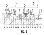
Fig. 2 is shown inFig. 3 . Apart from the fact that, for the sake of simplicity, the transistor ofFig. 3 comprises only onesource zone 19, transistor T1 is practically identical to T1 of the preceding example. Unlike the preceding example, in the embodiment shown inFig. 3 also transistor T2 comprises a cup-shaped p-type zone 30 which is situated within the region defined by the cup-shaped n-type zone 13. Said cup-shaped zone 30 comprises a buried p-type layer 30a, separated from the p-type substrate 10 by the buried n-type layer 13a, and a raisedwall 30b which extends from the surface to the buriedzone 30a in theepitaxial layer 11 and is separated from surrounding parts of the epitaxial layer by the n-type zone 13b. The transistors may be constructed substantially identically, with thebackgate region 18 of T2 bordering on the raisedwall 30b of the cup-shaped p-type zone 30 which is short-circuited to thesource zone 20 via thesource contact 28. The drain comprises a highly doped n-type zone 31 which is provided with adrain contact 32. The n-type cup-shapedzone 13 includes acontact 33 which, together with thedrain contact 32, is connected to Vdd. - During operation, the pn-junction between the cup-shaped
zones 13 and 30 may become forward-poled. The holes injected into thezone 13 will be retarded by the highly doped n-type zone 13, thus precluding diffusion of these holes to thesubstrate 10. In addition, a suitable choice of the doping concentration of thedrift region 16 of T2 enables also the high-side transistor to be constructed as a RESURF transistor, in a manner similar to that of the low-side transistor T1. - It will be obvious that the invention is not limited to the examples described hereinabove, and that within the scope of the invention as defined by the appended claims many variations are possible to those skilled in the art. For example, in the above-described examples, an n-type epitaxial layer can be used instead of a p-type layer. In addition, it is alternatively possible to provide the n-type drift regions in only a part, which borders on the highly-doped drain zones, of the regions surrounded by the cup-shaped zones, so that parts of the epitaxial layer around the backgate regions continue to be of the p-type. It is also possible to provide the transistors with a larger number of source regions forming an interdigital configuration with intermediate drain regions.
Claims (4)
- A semiconductor device comprising a half-bridge circuit with a first and a second n-channel DMOS transistor (T1,T2) forming a series connection between a terminal Vss for a low voltage and a terminal Vdd for a high voltage, which semiconductor device also comprises a semiconductor body with a p-type substrate (10) and, provided on said substrate, an epitaxial layer (11) in which, for the transistors, two separate regions are defined which are surrounded within the semiconductor body by two electrically insulated cup-shaped n-type zones (12,13) which each have a bottom (12a,13a) formed by a buried n-type zone at the interface between the substrate (10) and the epitaxial layer (11), and a raised wall (12b,13b) formed by an n-type zone which extends from an upper surface of the epitaxial layer (11) across the thickness of the epitaxial layer (11) to the underlying buried zone, each of the transistors comprising an n-type source and drain zone, the source zone (19,20) of each transistor being located in a p-type backgate region (17,18), the source zone (19) of the first transistor (T1) being connected to Vss and the drain zone being connected to the source zone (20) of the second transistor (T2) whose drain zone is connected to Vdd, characterized in that within the n-type cup-shaped zone (12) belonging to the first transistor (T1), a p-type cup-shaped zone (24) is formed whose bottom (24a) is formed by a p-type buried zone which is isolated from the substrate (10) by the buried n-type zone of the n-type cup-shaped zone (12), and the raised wall (24b) of said p-type cup-shaped zone (24) being formed by a p-type zone which extends from the upper surface of the epitaxial layer (11) to the buried p-type zone, the n-type source (19) and drain zones and a p-type backgate region (17) of the first transistor (T1) being arranged in the region surrounded by the p-type cup-shaped zone (24), and the n-type and p-type cup-shaped zones both being connected to the source zone and the backgate region and to Vss, and the n-type source and drain zones and a p-type backgate region of the second transistor (T2) being arranged in the region which is defined by the second n-type cup-shaped zone (13) and which is connected to Vdd.
- A semiconductor device as claimed in claim 1, characterized in that the epitaxial layer (11) is p-type, in which, in each of the regions defined by the cup-shaped zones (12,13), an n-type well is formed, the n-type well belonging to the first transistor (T1) being separated from the associated n-type cup-shaped zone (12) by the p-type cup-shaped zone (24), and the n-type well belonging to the second transistor (T2) being conductively connected to the associated n-type cup-shaped zone (13).
- A semiconductor device as claimed in claim 2, characterized in that the overall doping of the n-type well of the first transistor (T1), in a direction transverse to the surface, is, at least locally, at most 3.1012 atoms per cm2.
- A semiconductor device as claimed in any one of the preceding claims, characterized in that in the region defined by the n-type cup-shaped zone (13) belonging to the second transistor (T2), a p-type cup-shaped zone (30) is arranged having a bottom (30a) formed by a buried p-type zone which is separated from the p-type substrate by the intermediate bottom of the n-type cup-shaped zone, and having a raised wall (30b) formed by a p-type region extending from an upper surface of the epitaxial layer across the epitaxial layer to the buried p-type zone, the n-type source and drain zones and the p-type backgate region of the second transistor being formed in the region of the epitaxial layer surrounded by the cup-shaped p-type zone, and the source zone and the backgate region being jointly connected to the p-type cup-shaped zone.
Priority Applications (1)
| Application Number | Priority Date | Filing Date | Title |
|---|---|---|---|
| EP98945481A EP0978143B1 (en) | 1997-10-28 | 1998-10-12 | Semiconductor device comprising a half-bridge circuit |
Applications Claiming Priority (4)
| Application Number | Priority Date | Filing Date | Title |
|---|---|---|---|
| EP97203346 | 1997-10-28 | ||
| EP97203346 | 1997-10-28 | ||
| EP98945481A EP0978143B1 (en) | 1997-10-28 | 1998-10-12 | Semiconductor device comprising a half-bridge circuit |
| PCT/IB1998/001589 WO1999022409A2 (en) | 1997-10-28 | 1998-10-12 | Semiconductor device comprising a half-bridge circuit |
Publications (2)
| Publication Number | Publication Date |
|---|---|
| EP0978143A2 EP0978143A2 (en) | 2000-02-09 |
| EP0978143B1 true EP0978143B1 (en) | 2010-07-14 |
Family
ID=8228875
Family Applications (1)
| Application Number | Title | Priority Date | Filing Date |
|---|---|---|---|
| EP98945481A Expired - Lifetime EP0978143B1 (en) | 1997-10-28 | 1998-10-12 | Semiconductor device comprising a half-bridge circuit |
Country Status (6)
| Country | Link |
|---|---|
| US (1) | US6160304A (en) |
| EP (1) | EP0978143B1 (en) |
| JP (1) | JP2001507524A (en) |
| KR (1) | KR100664333B1 (en) |
| DE (1) | DE69841763D1 (en) |
| WO (1) | WO1999022409A2 (en) |
Families Citing this family (14)
| Publication number | Priority date | Publication date | Assignee | Title |
|---|---|---|---|---|
| KR100534601B1 (en) * | 1999-08-14 | 2005-12-07 | 한국전자통신연구원 | A power IC structure for simplifying fabrication process and characteristic control |
| US6737713B2 (en) * | 2001-07-03 | 2004-05-18 | Tripath Technology, Inc. | Substrate connection in an integrated power circuit |
| US6657274B2 (en) | 2001-10-11 | 2003-12-02 | Microsemi Corporation | Apparatus for controlling a high voltage circuit using a low voltage circuit |
| US6709900B2 (en) * | 2002-06-11 | 2004-03-23 | Texas Instruments Incorporated | Method of fabricating integrated system on a chip protection circuit |
| US6784493B2 (en) * | 2002-06-11 | 2004-08-31 | Texas Instruments Incorporated | Line self protecting multiple output power IC architecture |
| US6710427B2 (en) * | 2002-06-11 | 2004-03-23 | Texas Instruments Incorporated | Distributed power device with dual function minority carrier reduction |
| AU2003283750A1 (en) * | 2002-12-10 | 2004-06-30 | Koninklijke Philips Electronics N.V. | Integrated half-bridge power circuit |
| US7372685B2 (en) * | 2003-05-20 | 2008-05-13 | On Semiconductor | Multi-fault protected high side switch with current sense |
| US7125777B2 (en) * | 2004-07-15 | 2006-10-24 | Fairchild Semiconductor Corporation | Asymmetric hetero-doped high-voltage MOSFET (AH2MOS) |
| KR100834287B1 (en) * | 2006-12-27 | 2008-05-30 | 동부일렉트로닉스 주식회사 | Horizontal type MOS device and its manufacturing method |
| US7741680B2 (en) * | 2008-08-13 | 2010-06-22 | Analog Devices, Inc. | Electro-static discharge and latchup resistant semiconductor device |
| KR102163725B1 (en) | 2013-12-03 | 2020-10-08 | 삼성전자주식회사 | Semiconductor device and method of manufacturing the same |
| JP6326858B2 (en) * | 2014-02-24 | 2018-05-23 | セイコーエプソン株式会社 | Semiconductor device and manufacturing method thereof |
| CN109346466B (en) * | 2018-08-17 | 2020-10-16 | 矽力杰半导体技术(杭州)有限公司 | Semiconductor structure and driver chip |
Family Cites Families (13)
| Publication number | Priority date | Publication date | Assignee | Title |
|---|---|---|---|---|
| KR890001285Y1 (en) * | 1986-04-01 | 1989-03-31 | 김정인 | Advertising system |
| IT1197279B (en) * | 1986-09-25 | 1988-11-30 | Sgs Microelettronica Spa | INTEGRATED DEVICE TO SCREEN THE INJECTION OF CHARGES INTO THE SUBSTRATE, IN PARTICULAR IN PILOTING CIRCUITS OF INDUCTIVE AND / OR CAPACITIVE LOADS |
| JP2788269B2 (en) * | 1988-02-08 | 1998-08-20 | 株式会社東芝 | Semiconductor device and manufacturing method thereof |
| US5156989A (en) * | 1988-11-08 | 1992-10-20 | Siliconix, Incorporated | Complementary, isolated DMOS IC technology |
| EP0544048B1 (en) * | 1991-11-25 | 1997-06-18 | STMicroelectronics S.r.l. | Integrated bridge device optimising conduction power losses |
| EP0544047B1 (en) * | 1991-11-25 | 1998-02-18 | STMicroelectronics S.r.l. | High current MOS transistor integrated bridge structure optimising conduction power losses |
| IT1252623B (en) * | 1991-12-05 | 1995-06-19 | Sgs Thomson Microelectronics | SEMICONDUCTOR DEVICE INCLUDING AT LEAST A POWER TRANSISTOR AND AT LEAST A CONTROL CIRCUIT, WITH DYNAMIC INSULATION CIRCUIT, INTEGRATED IN A MONOLITHIC MANNER IN THE SAME PLATE |
| US5473183A (en) * | 1992-02-21 | 1995-12-05 | Sony Corporation | Semiconductor device of a first conductivity type which has a first well of a second conductivity type formed therein and a second well of the first conductivity type formed in the first well and a pair of MOSFET formed in the first and second wells |
| EP0559996B1 (en) * | 1992-03-12 | 1997-09-10 | STMicroelectronics S.r.l. | Drive circuit, particularly for power MOS half-bridges |
| US5286995A (en) * | 1992-07-14 | 1994-02-15 | Texas Instruments Incorporated | Isolated resurf LDMOS devices for multiple outputs on one die |
| US5373435A (en) * | 1993-05-07 | 1994-12-13 | Philips Electronics North America Corporation | High voltage integrated circuit driver for half-bridge circuit employing a bootstrap diode emulator |
| JP2715941B2 (en) * | 1994-10-31 | 1998-02-18 | 日本電気株式会社 | Method for manufacturing semiconductor device |
| US5834826A (en) * | 1997-05-08 | 1998-11-10 | Stmicroelectronics, Inc. | Protection against adverse parasitic effects in junction-isolated integrated circuits |
-
1998
- 1998-10-12 KR KR1019997005858A patent/KR100664333B1/en not_active IP Right Cessation
- 1998-10-12 WO PCT/IB1998/001589 patent/WO1999022409A2/en active IP Right Grant
- 1998-10-12 DE DE69841763T patent/DE69841763D1/en not_active Expired - Lifetime
- 1998-10-12 EP EP98945481A patent/EP0978143B1/en not_active Expired - Lifetime
- 1998-10-12 JP JP52356799A patent/JP2001507524A/en not_active Ceased
- 1998-10-27 US US09/179,284 patent/US6160304A/en not_active Expired - Lifetime
Also Published As
| Publication number | Publication date |
|---|---|
| WO1999022409A3 (en) | 1999-07-08 |
| KR20000069747A (en) | 2000-11-25 |
| DE69841763D1 (en) | 2010-08-26 |
| US6160304A (en) | 2000-12-12 |
| JP2001507524A (en) | 2001-06-05 |
| EP0978143A2 (en) | 2000-02-09 |
| WO1999022409A2 (en) | 1999-05-06 |
| KR100664333B1 (en) | 2007-01-02 |
Similar Documents
| Publication | Publication Date | Title |
|---|---|---|
| US6288424B1 (en) | Semiconductor device having LDMOS transistors and a screening layer | |
| US10002961B2 (en) | Semiconductor device suppressing current leakage in a bootstrap diode | |
| US5883413A (en) | Lateral high-voltage DMOS transistor with drain zone charge draining | |
| US6130458A (en) | Power IC having SOI structure | |
| KR100326475B1 (en) | Trench-gated mosfet with bidirectional voltage clamping | |
| US6825700B2 (en) | Semiconductor device | |
| US20120267750A1 (en) | Semiconductor apparatus | |
| EP0978143B1 (en) | Semiconductor device comprising a half-bridge circuit | |
| US6225664B1 (en) | Dielectrically isolated IC driver having upper-side and lower-side arm drivers and power IC having the same | |
| US6384431B1 (en) | Insulated gate bipolar transistor | |
| US20030025124A1 (en) | Circuit configuration for load-relieved switching | |
| US5473181A (en) | Integrated circuit arrangement having at least one power component and low-voltage components | |
| US6404015B2 (en) | Semiconductor device | |
| KR100278461B1 (en) | Semiconductor device and method of manufacturing the same | |
| US5556792A (en) | Process for manufacturing a power integrated circuit ("PIC") structure with a vertical IGBT | |
| US6914270B2 (en) | IGBT with PN insulation and production method | |
| US5412234A (en) | Integrated semiconductor circuit having improved breakdown voltage characteristics | |
| KR0136384B1 (en) | Semiconductor device | |
| US6979883B2 (en) | Integrated device in emitter-switching configuration and related manufacturing process | |
| US20230075374A1 (en) | Semiconductor-on-insulator device with lightly doped extension region | |
| EP4429110A1 (en) | High voltage semiconductor device with data transmission from a high voltage domain to a low voltage domain | |
| EP0580254A2 (en) | Integrated semiconductor circuit | |
| WO2021148383A1 (en) | Superjunction transistor device | |
| NL8902345A (en) | HV integrated circuit for intelligent power supply - uses buried layer and isolation barrier to reduce risk of short circuits |
Legal Events
| Date | Code | Title | Description |
|---|---|---|---|
| PUAI | Public reference made under article 153(3) epc to a published international application that has entered the european phase |
Free format text: ORIGINAL CODE: 0009012 |
|
| AK | Designated contracting states |
Kind code of ref document: A2 Designated state(s): DE FR GB IT NL |
|
| 17P | Request for examination filed |
Effective date: 20000110 |
|
| 17Q | First examination report despatched |
Effective date: 20061228 |
|
| RAP1 | Party data changed (applicant data changed or rights of an application transferred) |
Owner name: NXP B.V. |
|
| GRAP | Despatch of communication of intention to grant a patent |
Free format text: ORIGINAL CODE: EPIDOSNIGR1 |
|
| RIC1 | Information provided on ipc code assigned before grant |
Ipc: H01L 27/07 20060101ALI20100105BHEP Ipc: H01L 27/088 20060101ALI20100105BHEP Ipc: H01L 29/78 20060101AFI20100105BHEP |
|
| GRAS | Grant fee paid |
Free format text: ORIGINAL CODE: EPIDOSNIGR3 |
|
| GRAA | (expected) grant |
Free format text: ORIGINAL CODE: 0009210 |
|
| AK | Designated contracting states |
Kind code of ref document: B1 Designated state(s): DE FR GB IT NL |
|
| REG | Reference to a national code |
Ref country code: GB Ref legal event code: FG4D |
|
| REF | Corresponds to: |
Ref document number: 69841763 Country of ref document: DE Date of ref document: 20100826 Kind code of ref document: P |
|
| REG | Reference to a national code |
Ref country code: NL Ref legal event code: VDEP Effective date: 20100714 |
|
| PG25 | Lapsed in a contracting state [announced via postgrant information from national office to epo] |
Ref country code: NL Free format text: LAPSE BECAUSE OF FAILURE TO SUBMIT A TRANSLATION OF THE DESCRIPTION OR TO PAY THE FEE WITHIN THE PRESCRIBED TIME-LIMIT Effective date: 20100714 |
|
| PGFP | Annual fee paid to national office [announced via postgrant information from national office to epo] |
Ref country code: DE Payment date: 20101006 Year of fee payment: 13 |
|
| PLBE | No opposition filed within time limit |
Free format text: ORIGINAL CODE: 0009261 |
|
| STAA | Information on the status of an ep patent application or granted ep patent |
Free format text: STATUS: NO OPPOSITION FILED WITHIN TIME LIMIT |
|
| PG25 | Lapsed in a contracting state [announced via postgrant information from national office to epo] |
Ref country code: IT Free format text: LAPSE BECAUSE OF FAILURE TO SUBMIT A TRANSLATION OF THE DESCRIPTION OR TO PAY THE FEE WITHIN THE PRESCRIBED TIME-LIMIT Effective date: 20100714 |
|
| 26N | No opposition filed |
Effective date: 20110415 |
|
| REG | Reference to a national code |
Ref country code: DE Ref legal event code: R097 Ref document number: 69841763 Country of ref document: DE Effective date: 20110415 |
|
| PGFP | Annual fee paid to national office [announced via postgrant information from national office to epo] |
Ref country code: GB Payment date: 20110926 Year of fee payment: 14 |
|
| PGFP | Annual fee paid to national office [announced via postgrant information from national office to epo] |
Ref country code: FR Payment date: 20111118 Year of fee payment: 14 |
|
| GBPC | Gb: european patent ceased through non-payment of renewal fee |
Effective date: 20121012 |
|
| REG | Reference to a national code |
Ref country code: FR Ref legal event code: ST Effective date: 20130628 |
|
| PG25 | Lapsed in a contracting state [announced via postgrant information from national office to epo] |
Ref country code: DE Free format text: LAPSE BECAUSE OF NON-PAYMENT OF DUE FEES Effective date: 20130501 Ref country code: GB Free format text: LAPSE BECAUSE OF NON-PAYMENT OF DUE FEES Effective date: 20121012 |
|
| REG | Reference to a national code |
Ref country code: DE Ref legal event code: R119 Ref document number: 69841763 Country of ref document: DE Effective date: 20130501 |
|
| PG25 | Lapsed in a contracting state [announced via postgrant information from national office to epo] |
Ref country code: FR Free format text: LAPSE BECAUSE OF NON-PAYMENT OF DUE FEES Effective date: 20121031 |