EP0970397B1 - Optical demultiplexer comprising a diffraction grating - Google Patents
Optical demultiplexer comprising a diffraction grating Download PDFInfo
- Publication number
- EP0970397B1 EP0970397B1 EP97908417A EP97908417A EP0970397B1 EP 0970397 B1 EP0970397 B1 EP 0970397B1 EP 97908417 A EP97908417 A EP 97908417A EP 97908417 A EP97908417 A EP 97908417A EP 0970397 B1 EP0970397 B1 EP 0970397B1
- Authority
- EP
- European Patent Office
- Prior art keywords
- optical demultiplexer
- optical
- grating
- demultiplexer according
- crystalline material
- Prior art date
- Legal status (The legal status is an assumption and is not a legal conclusion. Google has not performed a legal analysis and makes no representation as to the accuracy of the status listed.)
- Expired - Lifetime
Links
Images

Classifications
-
- G—PHYSICS
- G02—OPTICS
- G02B—OPTICAL ELEMENTS, SYSTEMS OR APPARATUS
- G02B6/00—Light guides; Structural details of arrangements comprising light guides and other optical elements, e.g. couplings
- G02B6/10—Light guides; Structural details of arrangements comprising light guides and other optical elements, e.g. couplings of the optical waveguide type
- G02B6/12—Light guides; Structural details of arrangements comprising light guides and other optical elements, e.g. couplings of the optical waveguide type of the integrated circuit kind
- G02B6/122—Basic optical elements, e.g. light-guiding paths
- G02B6/124—Geodesic lenses or integrated gratings
Definitions
- the present invention relates to an optical diffraction grating suitable for use, for example, as a wavelength multiplexer/demultiplexer in an optical telecommunications system.
- WDM wavelength division multiplexing
- the grating is defined using photolithography and dry etched using, for example, chemically assisted ion-beam etching, to form a stepped wall extending perpendicularly through the planar waveguide.
- the grating is then metallised in order to improve its reflectivity.
- This structure offers only limited angular dispersion, and so is not able to accommodate many wavelength channels without becoming unacceptably large.
- EPA0365125 A2 relates to a one-dimensional reflective-type diffraction grating formed on a slab waveguide.
- an optical demultiplexer as specified in claim 1.
- photonic crystalline material denotes a material manufactured with a periodic variation in refractive index, having a periodicity of the order of magnitude of an optical wavelength. As further discussed below, such material is sometimes referred to as "photonic band gap material”.
- the present invention uses photonic crystalline material to provide a grating suitable for integration with other optical components and exhibiting high dispersion and efficiency.
- Photonic crystals are a class of material manufactured with a periodic dielectric structure. The behaviour of photons within such a structure is found to be analogous to that of electrons within a semiconductor. In particular it is found that there are photonic band gaps (PBGs) analogous to electronic band gaps in semiconductor crystals. Photons having wavelengths within the band gap range are forbidden to propagate. Most work on photonic crystals has focused on producing these photonic band gaps. However, a novel analysis by the present inventor has shown that photonic crystals exhibit another property which can be exploited to provide a highly efficient grating.
- PBGs photonic band gaps
- the pitch of the photonic crystal is selected so that the first order diffracted beam is grazingly emergent from the crystal, then the diffracted angle varies sharply with wavelength, while the diffracted beam has a relatively high output intensity, potentially equal to 20% or more of the input optical intensity.
- the region of photonic crystalline material is generally planar.
- the photonic crystalline material may comprise a generally regular array of scattering centres formed in a dielectric material, in which case preferably the array is a minimal array no more than 10 rows deep and preferably only 1, 2 or 3 rows deep.
- the scattering centres may comprise holes formed in a dielectric substrate.
- an effective diffraction grating can be formed from an array which is only a few rows deep. Where 2 or more rows are present, then preferably the spacing between the rows is such that, at a predetermined wavelength of operation, the grazingly emergent beam scattered from one row interferes constructively with the grazingly emergent beam scattered from the or each other row.
- the grating functions as a highly efficient fixed frequency filter and as such is particular valuable for use in WDM systems.
- the means for coupling light to and from the photonic crystalline material include waveguides formed on a common substrate with the photonic crystalline material.
- the waveguides may comprise planar structures, and may be arranged to confine light in the direction normal to the planar surface. It is particularly preferred that the waveguide should be a ridge waveguide arranged also to confine the beam in the plane parallel to the planar surface.
- the grating may be arranged to operate transmissively, with the waveguide for the input beam on one side of the photonic crystalline material, and the waveguide for the output be am on the other side of the photonic crystalline material.
- the grating may be arranged to function reflectively, in which case the means for coupling the input beams and means for coupling the grazingly emergent output beam are located on the same side of the photonic crystalline material.
- the dielectric material is a III-V material, and more preferably is indium phosphide.
- the photonic crystal may comprise a regular array formed from two dielectric materials of differing refractive indices.
- This structure may be formed as an array of holes in a first dielectric material with the holes filled with a second dielectric material.
- the substrate includes, e.g., a quaternary waveguide layer, then the holes may be filled with the same material used to form the basis of the substrate.
- An alternative structure may comprise pillars of a first dielectric material extending into air or into a second dielectric material.
- One of the dielectric materials making up the photonic crystal may have a refractive index which is variable in response to an applied control signal. This may be an electro-optic material responsive to an applied electrical field, or a non-linear optical material responsive to an applied optical control signal.
- the use of a material with a variable refractive index in the photonic crystal enables the grating to function as a tuneable filter.
- a grating comprises a region of photonic crystalline material 1 formed in a multi-layered planar substrate 2.
- An optical system comprising a first lens 31 with a focal length of, e.g. 10cm, and a second lens 32 with a focal length of, e.g. 1cm collimates an input optical beam.
- the lenses 31,32 are separated by a distance y which is equal to the sum of the focal lengths.
- the lens 32 is spaced from a facet of the planar substrate 2 by a distance z of 1 cm in this example.
- the optical system couples light into a waveguide layer 4 where it propagates to meet the photonic crystal 1 with normal incidence.
- a grazingly emergent diffracted beam is transmitted through the photonic crystal 1 and propagated through the waveguide layer 4 and emerges from a side facet of the planar substrate.
- the emergent beam tends to diverge in the direction normal to the planar substrate.
- a cylindrical lens may be used to collimate the emergent beam.
- Figure 2 shows schematically the configuration of the photonic crystal 1.
- the photonic crystal 1 comprises a linear array of holes formed in a substrate of dielectric constant 13 with a pitch of 0.57 ⁇ m.
- a normally incident input beam with a wavelength of around 1550 nm is diffracted by the photonic crystal to produce grazingly emergent transmitted and reflected beams.
- part of the beam passes straight through the photonic crystal without diffraction, and part is reflected.
- the width of the grating w is in this example 800 microns, the distance from the input fibre to the grating is 4mm and the distance from the grating to the.output is 4mm.
- the array may comprise a row of 1000 or more holes.
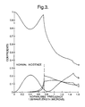
- Figure 3a shows the reflection and transmission coefficient for the normally incident beam as a function of frequency normalised to 1.55 ⁇ m.
- Plot a is the transmission coefficient
- b is the reflection coefficient
- plots c and d are the coefficients of the transmitted and reflected diffracted beams respectively.
- the onset of grazing emergence is seen in plots c and d at a normalised frequency of around 0.8 and is marked by the dashed line.
- the grazingly emergent beam at angles of a few degrees, say 3 to 5 degrees has a practically useful level of optical power and emerges at an angle which varies rapidly with wavelength.
- the grating may be used with a beam incident at an angle of, e.g., 30 degrees.
- Figure 3b shows the reflection and transmission coeffiecients in this case.
- the grazingly emergent output beam for a given wavelength will have different diffraction angles on either side of the normal to the plane of the photonic crystal.
- the pitch and hole size of the array, and the angle of incidence may be varied according to the refractive index of the substrate material and the desired wavelength range in which the grating is to be used.
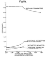
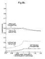
- Figures 8a and 8b are graphs showing the performance of gratings constructed with different pitches and angles of incidence.
- Figure 8a is for a grating with a pitch of 0.47 microns used at normal incidence.
- Figure 8b relates to a grating with a pitch of 0.313 microns used with a beam incident at an angle of 30 degrees to the normal.
- the hole radius in each case is 0.17 microns in 8a and 0.1175 microns in 8b. In both cases, the dielectric constant of the substrate is 10.9, giving a refractive index of 3.3.
- the holes need not have a circular cross section and may, for example, have a cross section which is generally square.
- the array of holes making up the photonic crystal are produced by reactive ion-beam etching (RIE) in a planar InP substrate.
- RIE reactive ion-beam etching
- Figure 5 shows in detail the structure of the planar substrate.
- the process of manufacture can be broken down into two stages: an epitaxy or deposition stage, and a subsequent stage in which the microstructure is etched.
- a waveguiding layer is fabricated on InP semiconductor material by a series of epitaxial depositions using the Metal-Organic Vapour Phase Epitaxy (MOVPE) technique.
- MOVPE Metal-Organic Vapour Phase Epitaxy
- microstructures are etched into the wafer. This is done using reactive ion etching. Direct write technology is used to create the mask directly on the sample.
- the second stage involves the following steps:
- FIG. 6 is a schematic of a photonic crystalline region formed in this manner.
- the holes in the waveguide are filled with a III-V semiconductor material such as InP itself, or a ternary e.g. GaInAs.
- the material used to fill the holes may have a refractive index which is variable in response to an applied control signal.
- it may comprise a liquid crystal material.
- the refractive index of the fill material then varies in response to a control voltage applied to a gate overlying the photonic crystal, allowing the grating to be tuned to a desired wavelength.
- the fill material may be, e.g., a semiconductor chosen to have a strong optical non-linearity. In this case its refractive index is controlled in response to an applied optical control signal.
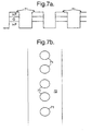
- Figures 7a and 7b show a further alternative structure for the photonic crystal.
- the scattering centres are pillars 71 of the substrate structure, extending into air.
- This structure may be produced by an RIE process as described above for the first example. The process is modified in that prior to the etching step, the silicon nitride photoresist is exposed everywhere except in the regions which are to form pillars. Then in the etching step, in the region 72 around the pillars the substrate is removed down to a depth of e.g. 0.7 microns leaving the pillars free-standing in a narrow trough in the substrate.
- the pillars and in previous examples the holes, have had a circular cross-section, this is not essential for the functioning of the grating, and that scattering centres having other less uniform shapes may be used.
- the cross-section may be generally ellipsoid, and may vary in size at different depths through the hole or pillar. This allows the use of etching processes which may not produce perfectly regular shapes.
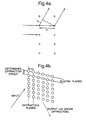
- Figure 4a shows schematically an example using 2 rows of holes, with the separation between the rows selected so that the path difference ⁇ is equal to an integer number of wavelengths, giving constructive interference of the diffracted beam for the design wavelength.
- the array pitch, wavelength and diffracted angle of the form ⁇ a cos ⁇ .
- the 2-dimensional structure can therefore be engineered to act as a fixed filter for one particular wavelength.
- the use of multiple rows of scattering centres is particularly preferred when the scattering centres are relatively weak in effect. This is the case if, for example, the holes etched in the substrate are relatively shallow and stop short of the waveguide layer or if they are filled with a second dielectric material having a refractive index close to that of the substrate. In this case more than a minimal array of holes may be required to produce a diffracted beam of sufficient power, and the array may be, for example, 10 or 15 rows deep.
- Figure 4b shows an example of a lattice which is 6 rows deep.
- This 2-D lattice has two main sets of parallel planes, one running vertically and the other running approximately horizontally.
- the lattice is designed to obtain non-zero order diffraction from one set of planes, and zeroth order diffraction from the other set.
- the condition is applied that both sets of planes should give rise to diffraction in the same direction. Therefore to obtain zero order diffraction (specular reflection), the planes running approximately horizontally should be angled such that their normal bisects the angle between the input beam and the output beam.
- the spacing of these planes is not critical, but it can be advantageous to space them so that the microstructures along the planes have a separation sufficiently small that only zero order diffraction results.
- the planes running approximately horizontally have in general a separation less than the separation of the microstructures in the 1-D array considered originally.
- the following condition applies for first order diffraction: sin ⁇ + sin ⁇ n ⁇ /d where n is the order, ⁇ is the wavelength, d is the separation of the planes or structures, and ⁇ and ⁇ are the angles of incidence of the incoming and outgoing beams.
- a structure which is formed in this way is not limited in operation to a single wavelength, but reinforces and diffracts different wavelengths through different angles. It is therefore suitable, for example, for use as a wavelength division mulitplexing (WDM) demultiplexer.
- WDM wavelength division mulitplexing
- the above discussion treats the photonic crystal as comprising weak scattering centres, producing Bragg diffraction.
- the scattering centres in general produce strong scattering.
- the present inventor has carried out a novel analysis of a one-dimensional array of strong scattering centres, which is set out below.
- G is a reciprocal lattice vector
- the equation for the plane wave coefficients, is where is the plane wave expansion of the inverse of ⁇ (r).
- the auxiliary equation for the plane wave coefficients of the y component of the magnetic field is
- the x axis is chosen to be perpendicular to the plane of the grating.
- To solve the wave equation (1) inside the grating one needs to find the possible components k x of the wavevector for propagation with fixed y component , k v ,and fixed frequency ⁇ .
- the equations (4) and (5) can be converted into an eigenvalue problem for k x From the solutions to this eigenvalue problem one can construct the general solution of the wave equation inside the grating by linear superposition and determine the coefficients by using the continuity of the electric field and its derivatives at the boundary of the grating.
- g is the y component of G.
- k ( k ⁇ ,K ( ⁇ ) / n ) with the ⁇ in the exponent denoting the sign of the imaginary part or in the case of the latter being zero it denotes the sign of the real part.
- k y k y ( 2 ⁇ / a 2 and ⁇ a is the dielectric constant of the material either side of the grating.
- b 1 and b 2 are the reciprocal lattice vectors defined by a i .
- b i 2 ⁇ ij .
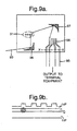
- Figure 9 shows a further alternative layout for a grating embodying the present invention.
- the grating is shown in use as a WDM demultiplexer, receiving a wavelength multiplex from an optical network and selecting 4 different output channels which are transmitted to local terminal equipment (not shown).
- local terminal equipment not shown
- the grating in this case is generally similar in construction to that of Figure 1. It includes a lens ended input fibre 93, a region 91 of photonic crystalline material, and an array of four lens-ended output fibres 95. It differs from the grating of Figure 1 in that concave mirrors 96,97 are used to route the input and output beams.
- the mirrors allow a more compact layout for the grating.
- the mirror 96 on the input side serves to collimate the beam incident on the grating, while the mirror 97 on the output side focuses the output beam onto an array of waveguides for the four different output channels.
- the mirrors may be formed during the course of an RIE process for forming the crystal as discussed above.
- the cross-hatched regions shown in the Figure are etched away to a depth of 1 to 1.5 microns, well below the depth of the waveguide layer. The impinging beam then undergoes total internal reflection at the curved boundary surface between the planar waveguide and air in the etched-away region.
- the input side mirror 96 is spaced from the grating by a distance of 3mm and the output side mirror is spaced from the grating by a similar distance.
- the beams reflected and focused by the output side mirror impinge upon an array 98 of ridge waveguides .
- the input end of the array is located at the focus of the mirror 97.
- Each waveguide is 3 microns wide and the separation between the centres of adjacent waveguides is 6 microns.
- the ridge in each waveguide is 0.5 microns high.
- the waveguides fan-out and are coupled at their output ends to the array of output fibre-waveguides 95 which carry the different channels on to different subscriber terminals.
- Figure 9b is a cross-section through the ridge waveguides on line XX of Figure 9b. The shaded region illustrates the optical mode confined under one of the ridges.
- Figure 10 illustrates for illustrative purposes only another possible stucture for an integrated WDM demultiplexer
- the microstructure 101 is curved and is used in reflection.
- This structure has the advantage that the concave layout of the microstructure eleimates the need for a collimating mirror or lens.
- the fabrication procedure described above allows the grating to be formed in any desired shape, including shapes which cannot be described by simple mathematical functions. The procedure makes possible precise control of the curvature of a microstructure in order to minimise optical aberrations.
- the grating structures described above may be configured to act as polarisation sensitive devices.
- the input beam is directed towards the grating as before.
- the reflected order is picked up, for example by an output waveguide arranged adjacent the input waveguide as in Figure 10.
- the ratio of reflection coefficients has a sharp peak as a function of the signal wavelength.
- This polarisation sensitivity may be exploited, for example, in the construction of a polarisation filter for use in the feedback loop of an active polarisation control system.
- the output from the filter passes to a photodetector and is used to drive a feedback circuit which drives electro-mechanical actuators to twist a fibre polariser.
- a desired polarisation state is maintained at the output of the optical system.
- the grating may also be used as a polarising beam splitter to separate orthogonal polarisation states, for example in coherent communications systems.
- microstructures of the present invention may be used in this context as part of an integrated planar optical receiver. Further, the microstructure of the invention may be used in all-optical switches of the type which employ orthogonally polarised switching and switched beams.
Landscapes
- Physics & Mathematics (AREA)
- Engineering & Computer Science (AREA)
- Microelectronics & Electronic Packaging (AREA)
- General Physics & Mathematics (AREA)
- Optics & Photonics (AREA)
- Optical Integrated Circuits (AREA)
Description
- The present invention relates to an optical diffraction grating suitable for use, for example, as a wavelength multiplexer/demultiplexer in an optical telecommunications system.
- Bulk optic diffraction gratings are well known, and it has previously been proposed to use such gratings as passive multiplexers/demultiplexers in optical networks employing wavelength division multiplexing (WDM). The use of bulk-optic components tends however to result in high packaging and maintenance costs. Accordingly, while the use of such components might be feasible if wavelength multiplexing/demultiplexing was to be confined to a few core switches, bulk optic components are not suitable for more widespread use in a network. Current interest in WDM centres on its use in local access networks in combination with optical time division multiplexing (OTDM) for longer links in the network. There remains a need therefore for a grating which is sufficiently robust and inexpensive to be used in local access loops throughout a network, and possibly to be present in each subscriber terminal.
- The paper by Poguntke and Soole, "Design of A Multistripe Array Grating Integrated Cavity (MAGIC) Laser", Journal of Light Wave Technology, Vol. 11 No. 12 December 1993, discloses a grating formed in an InP-based planar waveguide structure. The grating is defined using photolithography and dry etched using, for example, chemically assisted ion-beam etching, to form a stepped wall extending perpendicularly through the planar waveguide. The grating is then metallised in order to improve its reflectivity. This structure, however, offers only limited angular dispersion, and so is not able to accommodate many wavelength channels without becoming unacceptably large.
- EPA0365125 A2 relates to a one-dimensional reflective-type diffraction grating formed on a slab waveguide.
- According to the present invention, there is provided an optical demultiplexer as specified in claim 1.
- The term photonic crystalline material as used herein denotes a material manufactured with a periodic variation in refractive index, having a periodicity of the order of magnitude of an optical wavelength. As further discussed below, such material is sometimes referred to as "photonic band gap material".
- The present invention uses photonic crystalline material to provide a grating suitable for integration with other optical components and exhibiting high dispersion and efficiency. Photonic crystals are a class of material manufactured with a periodic dielectric structure. The behaviour of photons within such a structure is found to be analogous to that of electrons within a semiconductor. In particular it is found that there are photonic band gaps (PBGs) analogous to electronic band gaps in semiconductor crystals. Photons having wavelengths within the band gap range are forbidden to propagate. Most work on photonic crystals has focused on producing these photonic band gaps. However, a novel analysis by the present inventor has shown that photonic crystals exhibit another property which can be exploited to provide a highly efficient grating. It is found that if the pitch of the photonic crystal is selected so that the first order diffracted beam is grazingly emergent from the crystal, then the diffracted angle varies sharply with wavelength, while the diffracted beam has a relatively high output intensity, potentially equal to 20% or more of the input optical intensity.
- Preferably the region of photonic crystalline material is generally planar. The photonic crystalline material may comprise a generally regular array of scattering centres formed in a dielectric material, in which case preferably the array is a minimal array no more than 10 rows deep and preferably only 1, 2 or 3 rows deep. The scattering centres may comprise holes formed in a dielectric substrate.
- While work on photonic band gap materials has previously aimed at producing extensive 3-dimensional arrays, the present inventor has found that an effective diffraction grating can be formed from an array which is only a few rows deep. Where 2 or more rows are present, then preferably the spacing between the rows is such that, at a predetermined wavelength of operation, the grazingly emergent beam scattered from one row interferes constructively with the grazingly emergent beam scattered from the or each other row.
- When the separation between rows is chosen so that in a preferred scattering direction there is constructive interference, then the grating functions as a highly efficient fixed frequency filter and as such is particular valuable for use in WDM systems.
- The means for coupling light to and from the photonic crystalline material include waveguides formed on a common substrate with the photonic crystalline material. The waveguides may comprise planar structures, and may be arranged to confine light in the direction normal to the planar surface. It is particularly preferred that the waveguide should be a ridge waveguide arranged also to confine the beam in the plane parallel to the planar surface. The grating may be arranged to operate transmissively, with the waveguide for the input beam on one side of the photonic crystalline material, and the waveguide for the output be am on the other side of the photonic crystalline material.
- Alternatively, the grating may be arranged to function reflectively, in which case the means for coupling the input beams and means for coupling the grazingly emergent output beam are located on the same side of the photonic crystalline material.
- Preferably the dielectric material is a III-V material, and more preferably is indium phosphide.
- The photonic crystal may comprise a regular array formed from two dielectric materials of differing refractive indices. This structure may be formed as an array of holes in a first dielectric material with the holes filled with a second dielectric material. Alternatively, where the substrate includes, e.g., a quaternary waveguide layer, then the holes may be filled with the same material used to form the basis of the substrate. An alternative structure may comprise pillars of a first dielectric material extending into air or into a second dielectric material. One of the dielectric materials making up the photonic crystal may have a refractive index which is variable in response to an applied control signal. This may be an electro-optic material responsive to an applied electrical field, or a non-linear optical material responsive to an applied optical control signal.
- The use of a material with a variable refractive index in the photonic crystal enables the grating to function as a tuneable filter.
- Devices and methods of manufacture embodying the present invention will now be described in further detail, by way of example only, with reference to the accompanying drawings in which:
- Figures 1a and 1b are a plan and sectional side view respectively of a grating;
- Figure 2 is a diagram showing schematically the photonic crystal of the grating of Figure 1;
- Figures 3a and 3b are plots of reflection and transmission coefficients as a function of frequency for the photonic crystal of Figure 2;
- Figures 4a and 4b are schematics of alternative photonic crystal microstructures;
- Figure 5 is a cross-sectional view showing the structure of the planar substrate of the grating of Figure 1;
- Figure 6 is a schematic of a second alternative photonic crystal;
- Figures 7a and 7b are sectional and plan views of a third alternative photonic crystal;
- Figures 8a and 8b are plots of reflection and transmission coefficients of further examples of gratings embodying the present invention;
- Figures 9a and 9b are plan and sectional views of a WDM demultiplexer;
- Figure 10 is a plan view of a WDM multiplexer for illustrative purposes only;
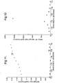
- Figure 11 is a plot showing the polarisation dependence of reflection coefficients of a grating embodying the present invention; and
- Figure 12 is a plot showing the ratio of the reflection coefficients of different polarisation states in the example of Figure 11.
-
- A grating comprises a region of photonic crystalline material 1 formed in a multi-layered planar substrate 2. An optical system comprising a first lens 31 with a focal length of, e.g. 10cm, and a second lens 32 with a focal length of, e.g. 1cm collimates an input optical beam. The lenses 31,32 are separated by a distance y which is equal to the sum of the focal lengths. The lens 32 is spaced from a facet of the planar substrate 2 by a distance z of 1 cm in this example. The optical system couples light into a waveguide layer 4 where it propagates to meet the photonic crystal 1 with normal incidence. A grazingly emergent diffracted beam is transmitted through the photonic crystal 1 and propagated through the waveguide layer 4 and emerges from a side facet of the planar substrate. The emergent beam tends to diverge in the direction normal to the planar substrate. Optionally a cylindrical lens may be used to collimate the emergent beam.
- Figure 2 shows schematically the configuration of the photonic crystal 1. For illustration, it comprises a linear array of holes formed in a substrate of dielectric constant 13 with a pitch of 0.57µm. As shown in the diagram, a normally incident input beam with a wavelength of around 1550 nm is diffracted by the photonic crystal to produce grazingly emergent transmitted and reflected beams. In addition, part of the beam passes straight through the photonic crystal without diffraction, and part is reflected. The width of the grating w is in this example 800 microns, the distance from the input fibre to the grating is 4mm and the distance from the grating to the.output is 4mm. For ease of illustration, only a relatively few holes are shown in the Figure. In practice, as further discussed below, the array may comprise a row of 1000 or more holes.
- Figure 3a shows the reflection and transmission coefficient for the normally incident beam as a function of frequency normalised to 1.55µm. Plot a is the transmission coefficient, b is the reflection coefficient and plots c and d are the coefficients of the transmitted and reflected diffracted beams respectively. The onset of grazing emergence is seen in plots c and d at a normalised frequency of around 0.8 and is marked by the dashed line. As set out in the theoretical analysis below, it is found that the grazingly emergent beam at angles of a few degrees, say 3 to 5 degrees, has a practically useful level of optical power and emerges at an angle which varies rapidly with wavelength.
- As an alternative to use with a normally incident beam, the grating may be used with a beam incident at an angle of, e.g., 30 degrees. Figure 3b shows the reflection and transmission coeffiecients in this case. In this case the grazingly emergent output beam for a given wavelength will have different diffraction angles on either side of the normal to the plane of the photonic crystal.
- The pitch and hole size of the array, and the angle of incidence, may be varied according to the refractive index of the substrate material and the desired wavelength range in which the grating is to be used. Figures 8a and 8b are graphs showing the performance of gratings constructed with different pitches and angles of incidence. Figure 8a is for a grating with a pitch of 0.47 microns used at normal incidence. Figure 8b relates to a grating with a pitch of 0.313 microns used with a beam incident at an angle of 30 degrees to the normal. The hole radius in each case is 0.17 microns in 8a and 0.1175 microns in 8b. In both cases, the dielectric constant of the substrate is 10.9, giving a refractive index of 3.3.
- The holes need not have a circular cross section and may, for example, have a cross section which is generally square.
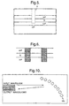
- In the present examples, the array of holes making up the photonic crystal are produced by reactive ion-beam etching (RIE) in a planar InP substrate. Figure 5 shows in detail the structure of the planar substrate.
- The process of manufacture can be broken down into two stages: an epitaxy or deposition stage, and a subsequent stage in which the microstructure is etched. In the first stage, a waveguiding layer is fabricated on InP semiconductor material by a series of epitaxial depositions using the Metal-Organic Vapour Phase Epitaxy (MOVPE) technique. This first stage includes the following steps:
- 1. A buffer layer of 1000nm thickness of InP is deposited;
- 2. A waveguiding layer 300nm thick of InGaAsP is deposited - the composition of the InGaAsP is such that it has a bandgap wavelength of approximately 1.3 microns;
- 3. A cladding layer 300nm thick of InP is deposited. All the deposited materials are nominally pure, i.e. undoped.
-
- Subsequently, in the second stage, microstructures are etched into the wafer. This is done using reactive ion etching. Direct write technology is used to create the mask directly on the sample. The second stage involves the following steps:
- 1. The sample is briefly cleaned in acid and then a 100nm thick layer of silicon nitride Si3N4 is deposited.
- 2. A layer of photoresist which is known as "ebeam resist" and which is sensitive to an electron beam is spun onto the sample to a thickness of approximately 500nm. In this case, the resist used is that manufactured by Nippon Zeon and known as ZEP520.
- 3. The resist is exposed in the desired microstructure pattern using electron beam lithography.
- 4. The resist is then developed. This dissolves the exposed areas. The unexposed ZEP520 remains and forms a mask which is used in the following stages.
- 5. Reactive ion etching using CF4 etches into the silicon nitride layer. This transfers the the mask pattern from the resist layer to the silicon nitride layer.
- 6. The sample is cleaned in two stages. The unexposed resist is removed, and then the polymer which results from the RIE process is removed.
- 7. The main RIE process is carried out. The patterned silicon nitride layer acts as a mask. The etching mixture consists of methane/hydrogen/oxygen. This mixture preferentially etches the InP/InGaAsP material over the silicon nitride mask.
- 8. The polymer resulting from the RIE process of step 7 is removed.
- 9. The sample is thinned from approximately 0.5mm thickness to approximately 150 microns thickness. This makes possible easier cleaving of individual samples. The individual samples are nominally 1x1 mm2. The grating microstructure bisects the samples parallel to the sides.
-
- It will be understood that the above process is described by way of example only, and that a variety of other processes may be used. For example, methane/hydrogen RIE may also be used. The etching may be followed by regrowth to fill the holes with a second dielectric material having a different refractive index to the substrate. Figure 6 is a schematic of a photonic crystalline region formed in this manner. In this example, the holes in the waveguide are filled with a III-V semiconductor material such as InP itself, or a ternary e.g. GaInAs. The material used to fill the holes may have a refractive index which is variable in response to an applied control signal. For example, it may comprise a liquid crystal material. The refractive index of the fill material then varies in response to a control voltage applied to a gate overlying the photonic crystal, allowing the grating to be tuned to a desired wavelength. Alternatively, the fill material may be, e.g., a semiconductor chosen to have a strong optical non-linearity. In this case its refractive index is controlled in response to an applied optical control signal.
- Figures 7a and 7b show a further alternative structure for the photonic crystal. In this example, the scattering centres are pillars 71 of the substrate structure, extending into air. This structure may be produced by an RIE process as described above for the first example. The process is modified in that prior to the etching step, the silicon nitride photoresist is exposed everywhere except in the regions which are to form pillars. Then in the etching step, in the region 72 around the pillars the substrate is removed down to a depth of e.g. 0.7 microns leaving the pillars free-standing in a narrow trough in the substrate. It should be noted that although in this example the pillars, and in previous examples the holes, have had a circular cross-section, this is not essential for the functioning of the grating, and that scattering centres having other less uniform shapes may be used. For example the cross-section may be generally ellipsoid, and may vary in size at different depths through the hole or pillar. This allows the use of etching processes which may not produce perfectly regular shapes.
- Figure 4a shows schematically an example using 2 rows of holes, with the separation between the rows selected so that the path difference δ is equal to an integer number of wavelengths, giving constructive interference of the diffracted beam for the design wavelength. This constraint can be expressed algebraically as λ = b(1-sin(90-)) where b is the separation between the rows and is the diffraction angle. It can been seen that the use of two more rows has the effect of adding a preferred direction to the diffraction. That is, while the simple 1-dimensional array either transmits or reflects the diffracted order, the modified 2-dimensional structure reinforces either the reflected or the transmitted order, depending on the distance b. A structure formed in this way functions as a fixed wavelength filter.
- For the 1-dimensional structure there is also a constraint on the array pitch, wavelength and diffracted angle of the form λ = a cos . Where a 2-dimensional structure is used, so that the constraint of the first equation above also applies, then there is a solution only for a single wavelength. The 2-dimensional structure can therefore be engineered to act as a fixed filter for one particular wavelength. The use of multiple rows of scattering centres is particularly preferred when the scattering centres are relatively weak in effect. This is the case if, for example, the holes etched in the substrate are relatively shallow and stop short of the waveguide layer or if they are filled with a second dielectric material having a refractive index close to that of the substrate. In this case more than a minimal array of holes may be required to produce a diffracted beam of sufficient power, and the array may be, for example, 10 or 15 rows deep.
- Figure 4b shows an example of a lattice which is 6 rows deep. This 2-D lattice has two main sets of parallel planes, one running vertically and the other running approximately horizontally. The lattice is designed to obtain non-zero order diffraction from one set of planes, and zeroth order diffraction from the other set. The condition is applied that both sets of planes should give rise to diffraction in the same direction. Therefore to obtain zero order diffraction (specular reflection), the planes running approximately horizontally should be angled such that their normal bisects the angle between the input beam and the output beam. The spacing of these planes is not critical, but it can be advantageous to space them so that the microstructures along the planes have a separation sufficiently small that only zero order diffraction results. The planes running approximately horizontally have in general a separation less than the separation of the microstructures in the 1-D array considered originally. The following condition applies for first order diffraction:
- For the purposes of illustration, the above discussion treats the photonic crystal as comprising weak scattering centres, producing Bragg diffraction. In reality, the scattering centres in general produce strong scattering. The present inventor has carried out a novel analysis of a one-dimensional array of strong scattering centres, which is set out below.
- The derivation of the dispersion equation for a planar photonic crystal will first be described. Let k i and k d be the wavevectors for the incident and diffracted waves and g a reciprocal lattice vector for the periodic variation of the refractive index which is the essential aspect of the grating. Because the electromagnetic fields that constitute the incident and diffracted waves must belong to the same irreducible representation of the group of translational symmetry operations for the grating, then
- The calculation of field intensities for the reflected transmitted and diffracted beams will now be described. A grating will only be useful at grazing emergence if the grating diffracts sufficient optical power. A measure of this is the square of the electric field in the diffracted beam compared with that in the incident beam. Such calculations have been performed for a single line of air cylinders in indium phosphide for the electric field polarised along the axes of the cylinders, which is taken as the z axis in a Cartesian coordinate system. The wave equation for the electric field E(x,y) derived from the Maxwell equations for propagation in the (x, y) plane, at angular frequency ω, iswhere G is a reciprocal lattice vector and the equation for the plane wave coefficients,
 , is
, is where
where is the plane wave expansion of the inverse of ε(r). The auxiliary equation for the plane wave coefficients of the y component of the magnetic field is
 The x axis is chosen to be perpendicular to the plane of the grating. To solve the wave equation (1) inside the grating one needs to find the possible components k x of the wavevector for propagation with fixed y component , k v ,and fixed frequency ω. The equations (4) and (5) can be converted into an eigenvalue problem for k x
 From the solutions to this eigenvalue problem one can construct the general solution of the wave equation inside the grating by linear superposition and determine the coefficients by using the continuity of the electric field and its derivatives at the boundary of the grating. The resultant set of linear equations obtained is, in partitioned matrix form,
 where
where and the integers ng1 and ng2 are defined by G = ng1bt + ng2b2. g is the y component of G.
K (±) / g and K (±) / n, the z component of the wavevectors of the plane wave solutions outside the grating are defined by - k = (k γ ,K (±) / n) with the ± in the exponent denoting the sign of the imaginary part or in the case of the latter being zero it denotes the sign of the real part. k y =
k y (2π / a 2 and ε a is the dielectric constant of the material either side of the grating. - a1 = (a 1x ,a 1y ) and a2 = (0,a 2) are the lattice vectors of the photonic crystal of which the grating is made. b1 and b2 are the reciprocal lattice vectors defined by a i .b i = 2πδ ij .
- The equation (7) is written explicitly for the case in which the grating is just one period of the photonic crystal thick and the origin of coordinates is taken at the centre of the grating layer.
- The equations derived above will now be applied to illustrate the effectiveness of one example of a WDM grating embodying the present invention. Assuming normal incidence, ϑ d denotes angle of diffracted beam makes with normal to grating. If λ is the wavelength of the light in the medium (either side of the grating) and a is the pitch of the grating, then sin(ϑ d ) = λ / a. For near grazing, emergence ϑ d is close to 90° and it convenient to write ϑ d = π / 2- where is small. Using sin d = cos ≈ 1 - 1 / 2 2 we can easily derive the angle of emergence as a function of wavelength λ ie
- Figure 9 shows a further alternative layout for a grating embodying the present invention. In this example the grating is shown in use as a WDM demultiplexer, receiving a wavelength multiplex from an optical network and selecting 4 different output channels which are transmitted to local terminal equipment (not shown). Such a configuration might be used, for example, in a local access node in a broadband optical telecommunications network. The grating in this case is generally similar in construction to that of Figure 1. It includes a lens ended input fibre 93, a region 91 of photonic crystalline material, and an array of four lens-ended output fibres 95. It differs from the grating of Figure 1 in that concave mirrors 96,97 are used to route the input and output beams. The mirrors allow a more compact layout for the grating. The mirror 96 on the input side serves to collimate the beam incident on the grating, while the mirror 97 on the output side focuses the output beam onto an array of waveguides for the four different output channels. The mirrors may be formed during the course of an RIE process for forming the crystal as discussed above. The cross-hatched regions shown in the Figure are etched away to a depth of 1 to 1.5 microns, well below the depth of the waveguide layer. The impinging beam then undergoes total internal reflection at the curved boundary surface between the planar waveguide and air in the etched-away region. In this example, the input side mirror 96 is spaced from the grating by a distance of 3mm and the output side mirror is spaced from the grating by a similar distance. The beams reflected and focused by the output side mirror impinge upon an array 98 of ridge waveguides . The input end of the array is located at the focus of the mirror 97. Each waveguide is 3 microns wide and the separation between the centres of adjacent waveguides is 6 microns. The ridge in each waveguide is 0.5 microns high. The waveguides fan-out and are coupled at their output ends to the array of output fibre-waveguides 95 which carry the different channels on to different subscriber terminals. Figure 9b is a cross-section through the ridge waveguides on line XX of Figure 9b. The shaded region illustrates the optical mode confined under one of the ridges.
- Figure 10 illustrates for illustrative purposes only another possible stucture for an integrated WDM demultiplexer In this example, the microstructure 101 is curved and is used in reflection. This structure has the advantage that the concave layout of the microstructure eleimates the need for a collimating mirror or lens. The fabrication procedure described above allows the grating to be formed in any desired shape, including shapes which cannot be described by simple mathematical functions. The procedure makes possible precise control of the curvature of a microstructure in order to minimise optical aberrations.
- The grating structures described above may be configured to act as polarisation sensitive devices. In this case the input beam is directed towards the grating as before. Now, however the reflected order is picked up, for example by an output waveguide arranged adjacent the input waveguide as in Figure 10. One polarisation state is found to be reflected far more strongly than the other. Figure 11 shows the reflection coefficients for the TM (transverse magnetic) and TE (transverse electric) polarisation modes in the case of a structure comprising one layer of circular holes with a pitch of 0.46 microns, incident at an angle theta such that sin (theta)=0.05. As shown in Figure 12, the ratio of reflection coefficients has a sharp peak as a function of the signal wavelength. This polarisation sensitivity may be exploited, for example, in the construction of a polarisation filter for use in the feedback loop of an active polarisation control system. In such a system the output from the filter passes to a photodetector and is used to drive a feedback circuit which drives electro-mechanical actuators to twist a fibre polariser. In this way a desired polarisation state is maintained at the output of the optical system. The grating may also be used as a polarising beam splitter to separate orthogonal polarisation states, for example in coherent communications systems. In quantum cryptographic key distribution systems, such as those described in the present applicant's international patent application WO 94/15422, polarisation-sensitive detection is required, and the microstructures of the present invention may be used in this context as part of an integrated planar optical receiver. Further, the microstructure of the invention may be used in all-optical switches of the type which employ orthogonally polarised switching and switched beams.
Claims (15)
- An optical demultiplexer for wavelength multiplexed optical signals, including an optical diffraction arrangement, the optical diffraction arrangement comprising:a) a region of photonic crystalline material, for performing diffraction;b) input coupling means having an input optical waveguide for coupling an input beam to the photonic crystalline material; andc) output coupling means having at least one output optical waveguide, wherein the or each output optical waveguide and the input optical waveguide are formed on a common substrate with the photonic crystalline material, characterised in that the output coupling means is arranged to receive a grazingly emergent beam from the photonic crystalline material, wherein the photonic crystalline material comprises a generally regular array of scattering centres formed in a dielectric material, the generally regular array having a plurality of rows.
- An optical demultiplexer according to claim 1, in which the region of photonic crystalline material is formed in a waveguiding layer of dielectric material.
- An optical demultiplexer according to claim 1 or claim 2, wherein the array is formed by a no more than 10 rows of scattering centres.
- An optical demultiplexer according to any preceding claim, in which the waveguides comprise planar structures arranged to confine light in the direction normal to the planar surface.
- An optical demultiplexer according to claim 4, in which at least one of the waveguides comprises a ridge waveguide arranged to confine light also in the direction parallel to the planar surface.
- An optical demultiplexer according to any one of the preceding claims, in which the grating is configured to operate transmissively, with the means for coupling an input beam and the mean for coupling an output beam located on either side of the photonic crystalline material.
- An optical demultiplexer according to any one of the preceding claims, in which the dielectric material is a III-V material.
- An optical demultiplexer according to claim 7, in which the dielectric material is indium phosphide.
- An optical demultiplexer according to any preceding claim in which the scattering centres comprise holes formed in the dielectric substrate.
- An optical demultiplexer according to claim 9, in which the holes are filled with a dielectric material.
- An optical demultiplexer according to any one of the preceding claims, in which the means for coupling an input beam include means for collimating a beam incident on the region of photonic crystalline material.
- An optical demultiplexer according to any one of the preceding claims, in which the means for coupling an output beam include means for focussing the grazingly emergent output beam.
- An optical demultiplexer according to claim 11 or 12, in which at least one of the means for collimating and the means for focussing comprises a convex reflective surface formed integrally in a common substrate with the region of photonic crystalline material.
- An optical demultiplexer as claimed in any preceding claim wherein the region of photonic crystalline material forms a diffraction grating, and wherein the grazingly emergent beam is emergent, in use, at a grazing angle to the grating, the grazing angle being between three and five degrees.
- An optical demultiplexer as claimed in any preceding, wherein the output coupling means includes a plurality of waveguides, each arranged to receive a respective wavelength channel.
Priority Applications (1)
| Application Number | Priority Date | Filing Date | Title |
|---|---|---|---|
| EP97908417A EP0970397B1 (en) | 1996-03-27 | 1997-03-24 | Optical demultiplexer comprising a diffraction grating |
Applications Claiming Priority (4)
| Application Number | Priority Date | Filing Date | Title |
|---|---|---|---|
| EP96302115 | 1996-03-27 | ||
| EP96302115 | 1996-03-27 | ||
| EP97908417A EP0970397B1 (en) | 1996-03-27 | 1997-03-24 | Optical demultiplexer comprising a diffraction grating |
| PCT/GB1997/000817 WO1997036198A1 (en) | 1996-03-27 | 1997-03-24 | Optical diffraction grating |
Publications (2)
| Publication Number | Publication Date |
|---|---|
| EP0970397A1 EP0970397A1 (en) | 2000-01-12 |
| EP0970397B1 true EP0970397B1 (en) | 2005-06-29 |
Family
ID=8224863
Family Applications (1)
| Application Number | Title | Priority Date | Filing Date |
|---|---|---|---|
| EP97908417A Expired - Lifetime EP0970397B1 (en) | 1996-03-27 | 1997-03-24 | Optical demultiplexer comprising a diffraction grating |
Country Status (7)
| Country | Link |
|---|---|
| US (1) | US6052213A (en) |
| EP (1) | EP0970397B1 (en) |
| JP (1) | JP2000508083A (en) |
| AU (1) | AU2038897A (en) |
| CA (1) | CA2248042C (en) |
| DE (1) | DE69733670T2 (en) |
| WO (1) | WO1997036198A1 (en) |
Families Citing this family (61)
| Publication number | Priority date | Publication date | Assignee | Title |
|---|---|---|---|---|
| DE19745324C2 (en) * | 1997-10-14 | 1999-09-16 | Deutsche Telekom Ag | Method and device for wavelength-selective mixing and / or distribution of polychromatic light |
| US6134369A (en) * | 1999-03-31 | 2000-10-17 | Matsushita Electric Industrial Co. | Compact optical waveguide |
| JP2001075040A (en) * | 1999-09-02 | 2001-03-23 | Ricoh Co Ltd | Laser scanning system |
| US7167615B1 (en) * | 1999-11-05 | 2007-01-23 | Board Of Regents, The University Of Texas System | Resonant waveguide-grating filters and sensors and methods for making and using same |
| US8111401B2 (en) * | 1999-11-05 | 2012-02-07 | Robert Magnusson | Guided-mode resonance sensors employing angular, spectral, modal, and polarization diversity for high-precision sensing in compact formats |
| JP2001141946A (en) * | 1999-11-16 | 2001-05-25 | Oki Electric Ind Co Ltd | Multiplexing and demultiplexing element |
| JP2001272557A (en) * | 2000-03-27 | 2001-10-05 | Minolta Co Ltd | Optical functional element and its manufacturing method |
| US6654533B1 (en) | 2000-06-16 | 2003-11-25 | Metrophotonics Inc. | Polarization independent waveguide structure |
| US6813064B2 (en) * | 2000-07-24 | 2004-11-02 | Sajeev John | Electro-actively tunable photonic bandgap materials |
| US20020027655A1 (en) * | 2000-09-04 | 2002-03-07 | Shigeo Kittaka | Optical device and spectroscopic and polarization separating apparatus using the same |
| US7875434B2 (en) * | 2000-10-30 | 2011-01-25 | Sru Biosystems, Inc. | Label-free methods for performing assays using a colorimetric resonant reflectance optical biosensor |
| US7300803B2 (en) * | 2000-10-30 | 2007-11-27 | Sru Biosystems, Inc. | Label-free methods for performing assays using a colorimetric resonant reflectance optical biosensor |
| US7023544B2 (en) * | 2000-10-30 | 2006-04-04 | Sru Biosystems, Inc. | Method and instrument for detecting biomolecular interactions |
| US7264973B2 (en) * | 2000-10-30 | 2007-09-04 | Sru Biosystems, Inc. | Label-free methods for performing assays using a colorimetric resonant optical biosensor |
| US7142296B2 (en) * | 2000-10-30 | 2006-11-28 | Sru Biosystems, Inc. | Method and apparatus for detecting biomolecular interactions |
| US7217574B2 (en) * | 2000-10-30 | 2007-05-15 | Sru Biosystems, Inc. | Method and apparatus for biosensor spectral shift detection |
| US7101660B2 (en) | 2000-10-30 | 2006-09-05 | Sru Biosystems, Inc. | Method for producing a colorimetric resonant reflection biosensor on rigid surfaces |
| US7615339B2 (en) * | 2000-10-30 | 2009-11-10 | Sru Biosystems, Inc. | Method for producing a colorimetric resonant reflection biosensor on rigid surfaces |
| US7175980B2 (en) * | 2000-10-30 | 2007-02-13 | Sru Biosystems, Inc. | Method of making a plastic colorimetric resonant biosensor device with liquid handling capabilities |
| US7306827B2 (en) | 2000-10-30 | 2007-12-11 | Sru Biosystems, Inc. | Method and machine for replicating holographic gratings on a substrate |
| US7575939B2 (en) * | 2000-10-30 | 2009-08-18 | Sru Biosystems, Inc. | Optical detection of label-free biomolecular interactions using microreplicated plastic sensor elements |
| US7153702B2 (en) | 2000-10-30 | 2006-12-26 | Sru Biosystems, Inc. | Label-free methods for performing assays using a colorimetric resonant reflectance optical biosensor |
| US6951715B2 (en) * | 2000-10-30 | 2005-10-04 | Sru Biosystems, Inc. | Optical detection of label-free biomolecular interactions using microreplicated plastic sensor elements |
| US7070987B2 (en) * | 2000-10-30 | 2006-07-04 | Sru Biosystems, Inc. | Guided mode resonant filter biosensor using a linear grating surface structure |
| US7202076B2 (en) | 2000-10-30 | 2007-04-10 | Sru Biosystems, Inc. | Label-free high-throughput optical technique for detecting biomolecular interactions |
| US20030113766A1 (en) * | 2000-10-30 | 2003-06-19 | Sru Biosystems, Llc | Amine activated colorimetric resonant biosensor |
| US7118710B2 (en) * | 2000-10-30 | 2006-10-10 | Sru Biosystems, Inc. | Label-free high-throughput optical technique for detecting biomolecular interactions |
| US7371562B2 (en) * | 2000-10-30 | 2008-05-13 | Sru Biosystems, Inc. | Guided mode resonant filter biosensor using a linear grating surface structure |
| US20030092075A1 (en) * | 2000-10-30 | 2003-05-15 | Sru Biosystems, Llc | Aldehyde chemical surface activation processes and test methods for colorimetric resonant sensors |
| JP2002303836A (en) | 2001-04-04 | 2002-10-18 | Nec Corp | Optical switch with photonic crystal structure |
| US6466709B1 (en) * | 2001-05-02 | 2002-10-15 | California Institute Of Technology | Photonic crystal microcavities for strong coupling between an atom and the cavity field and method of fabricating the same |
| DE10121462A1 (en) * | 2001-05-02 | 2002-11-21 | Infineon Technologies Ag | grid array |
| WO2003034118A1 (en) * | 2001-10-17 | 2003-04-24 | Risø National Laboratory | A system for electromagnetic field conversion |
| US6721476B2 (en) | 2001-12-03 | 2004-04-13 | Honeywell International Inc. | Optical demultiplexer based on three-dimensionally periodic photonic crystals |
| US20030123827A1 (en) * | 2001-12-28 | 2003-07-03 | Xtalight, Inc. | Systems and methods of manufacturing integrated photonic circuit devices |
| US6991847B2 (en) | 2002-02-07 | 2006-01-31 | Honeywell International Inc. | Light emitting photonic crystals |
| AU2003224626A1 (en) * | 2002-03-07 | 2003-09-22 | The Government Of The United States Of America As Represented By Thesecretary Of The Navy | Photonic-crystal distributed-feedback and distributed-bragg reflector lasers |
| US6649990B2 (en) * | 2002-03-29 | 2003-11-18 | Intel Corporation | Method and apparatus for incorporating a low contrast interface and a high contrast interface into an optical device |
| US7429492B2 (en) * | 2002-09-09 | 2008-09-30 | Sru Biosystems, Inc. | Multiwell plates with integrated biosensors and membranes |
| US7927822B2 (en) | 2002-09-09 | 2011-04-19 | Sru Biosystems, Inc. | Methods for screening cells and antibodies |
| US7309614B1 (en) | 2002-12-04 | 2007-12-18 | Sru Biosystems, Inc. | Self-referencing biodetection method and patterned bioassays |
| US8298780B2 (en) * | 2003-09-22 | 2012-10-30 | X-Body, Inc. | Methods of detection of changes in cells |
| CA2544836A1 (en) * | 2003-11-06 | 2005-05-26 | Guo Bin Wang | High-density amine-functionalized surface |
| DE102004050418B4 (en) * | 2004-10-15 | 2008-08-14 | Yokogawa Electric Corporation, Musashino | Active diffraction grating |
| WO2007050058A1 (en) * | 2005-10-25 | 2007-05-03 | Georgia Tech Research Corporation | Spatial separation of optical frefquency components using photonic crystals |
| CN100462747C (en) * | 2005-12-27 | 2009-02-18 | 中国科学院光电技术研究所 | A three-step beam splitting grating and its manufacturing method |
| DE102006046131B4 (en) * | 2006-09-28 | 2020-06-25 | X-Fab Semiconductor Foundries Ag | Process for manufacturing an optical interface for integrated optical applications |
| JP2010508520A (en) * | 2006-10-31 | 2010-03-18 | エス アール ユー バイオシステムズ,インコーポレイテッド | Method for blocking non-specific protein binding on functionalized surfaces |
| CA2683082A1 (en) * | 2007-04-19 | 2008-10-30 | Sru Biosystems, Inc. | Method for employing a biosensor to detect small molecules that bind directly to immobilized targets |
| US7587103B2 (en) * | 2007-07-09 | 2009-09-08 | Lawrence Livermore National Security, Llc | Method for ultrafast optical deflection enabling optical recording via serrated or graded light illumination |
| US9134307B2 (en) * | 2007-07-11 | 2015-09-15 | X-Body, Inc. | Method for determining ion channel modulating properties of a test reagent |
| AU2008274978A1 (en) * | 2007-07-11 | 2009-01-15 | Sru Biosystems, Inc. | Methods of identifying modulators of ion channels |
| US8244083B2 (en) * | 2007-09-17 | 2012-08-14 | Seidman Abraham N | Steerable, thin far-field electromagnetic beam |
| US8257936B2 (en) * | 2008-04-09 | 2012-09-04 | X-Body Inc. | High resolution label free analysis of cellular properties |
| WO2009149285A1 (en) * | 2008-06-04 | 2009-12-10 | Sru Biosystems, Inc. | Detection of promiscuous small submicrometer aggregates |
| US20100273185A1 (en) * | 2009-04-27 | 2010-10-28 | Sru Biosystems, Inc. | Detection of Biased Agonist Activation |
| EP2430448A1 (en) * | 2009-05-15 | 2012-03-21 | SRU Biosystems, Inc. | Detection of changes in cell populations and mixed cell populations |
| JP2013523095A (en) * | 2010-03-26 | 2013-06-17 | エックス−ボディ インコーポレイテッド | Use of induced pluripotent cells and other cells to screen compound libraries |
| WO2013049942A1 (en) | 2011-10-06 | 2013-04-11 | Valorbec S.E.C. | High efficiency mono-order concave diffraction grating |
| KR101602418B1 (en) * | 2012-04-06 | 2016-03-10 | 코닝정밀소재 주식회사 | Substrate for oled with enhanced light extraction efficiency, method for fabricating thereof and oled having the same |
| EP2741074A1 (en) | 2012-12-04 | 2014-06-11 | F. Hoffmann-La Roche AG | Device for use in the detection of binding affinities |
Family Cites Families (6)
| Publication number | Priority date | Publication date | Assignee | Title |
|---|---|---|---|---|
| FR2579044B1 (en) * | 1985-03-13 | 1988-02-26 | Commissariat Energie Atomique | DEVICE FOR MULTIPLEXING MULTIPLE LIGHT SIGNALS IN INTEGRATED OPTICS |
| GB2222891B (en) * | 1988-09-17 | 1992-01-08 | Stc Plc | Diffraction grating |
| US5245466A (en) * | 1990-08-15 | 1993-09-14 | President And Fellows Of Harvard University And Rowland Institute | Optical matter |
| US5187461A (en) * | 1991-02-15 | 1993-02-16 | Karl Brommer | Low-loss dielectric resonator having a lattice structure with a resonant defect |
| EP0678196B1 (en) * | 1993-01-08 | 2002-04-10 | Massachusetts Institute Of Technology | Low-loss optical and optoelectronic integrated circuits |
| US5726805A (en) * | 1996-06-25 | 1998-03-10 | Sandia Corporation | Optical filter including a sub-wavelength periodic structure and method of making |
-
1997
- 1997-03-24 EP EP97908417A patent/EP0970397B1/en not_active Expired - Lifetime
- 1997-03-24 WO PCT/GB1997/000817 patent/WO1997036198A1/en not_active Ceased
- 1997-03-24 DE DE69733670T patent/DE69733670T2/en not_active Expired - Fee Related
- 1997-03-24 CA CA002248042A patent/CA2248042C/en not_active Expired - Fee Related
- 1997-03-24 AU AU20388/97A patent/AU2038897A/en not_active Abandoned
- 1997-03-24 JP JP9534136A patent/JP2000508083A/en active Pending
- 1997-03-24 US US09/051,537 patent/US6052213A/en not_active Expired - Lifetime
Non-Patent Citations (1)
| Title |
|---|
| POGUNTKE ET AL, J. LIGHTWAVE TECHNOL, vol. 11, no. 12, December 1993 (1993-12-01), pages 2191 - 2200, XP000422683 * |
Also Published As
| Publication number | Publication date |
|---|---|
| DE69733670D1 (en) | 2005-08-04 |
| EP0970397A1 (en) | 2000-01-12 |
| CA2248042C (en) | 2002-04-23 |
| AU2038897A (en) | 1997-10-17 |
| CA2248042A1 (en) | 1997-10-02 |
| US6052213A (en) | 2000-04-18 |
| JP2000508083A (en) | 2000-06-27 |
| DE69733670T2 (en) | 2006-04-20 |
| WO1997036198A1 (en) | 1997-10-02 |
Similar Documents
| Publication | Publication Date | Title |
|---|---|---|
| EP0970397B1 (en) | Optical demultiplexer comprising a diffraction grating | |
| Kosaka et al. | Superprism phenomena in photonic crystals: Toward microscale lightwave circuits | |
| Halir et al. | Subwavelength-grating metamaterial structures for silicon photonic devices | |
| US5937115A (en) | Switchable optical components/structures and methods for the fabrication thereof | |
| US6999156B2 (en) | Tunable subwavelength resonant grating filter | |
| EP1353200B1 (en) | Diffraction grating based fibre-to-waveguide coupler for polarisation independent photonic integrated circuits | |
| US5937113A (en) | Optical grating-based device having a slab waveguide polarization compensating region | |
| US5970190A (en) | Grating-in-etalon polarization insensitive wavelength division multiplexing devices | |
| US6735368B2 (en) | Optical delay device | |
| EP1560048B9 (en) | Optical isolator utilizing a micro-resonator | |
| US5640474A (en) | Easily manufacturable optical self-imaging waveguide | |
| US6385376B1 (en) | Fused vertical coupler for switches, filters and other electro-optic devices | |
| US20030013304A1 (en) | Method for forming passive optical coupling device | |
| US5581639A (en) | Raman-nath diffraction grating | |
| US7881571B2 (en) | Coupling device with compensated birefringence | |
| US20040258355A1 (en) | Micro-structure induced birefringent waveguiding devices and methods of making same | |
| US20030206694A1 (en) | Photonic multi-bandgap lightwave device and methods for manufacturing thereof | |
| US4775206A (en) | Separation structure, optical switching element including such structures and optical switching matrix constituted by these switching elements | |
| US6654533B1 (en) | Polarization independent waveguide structure | |
| WO2003062909A2 (en) | Polarisation converter | |
| JPH0992933A (en) | Wavelength changeable semiconductor laser | |
| Cremer et al. | Bragg gratings on InGaAsP/InP waveguides as polarization independent optical filters | |
| Minier et al. | Superimposed phase gratings in planar optical waveguides for wavelength demultiplexing applications | |
| EP0947860A2 (en) | Optical grating-based device having a slab waveguide polarization compensating region | |
| WO2000048025A1 (en) | Optical components |
Legal Events
| Date | Code | Title | Description |
|---|---|---|---|
| PUAI | Public reference made under article 153(3) epc to a published international application that has entered the european phase |
Free format text: ORIGINAL CODE: 0009012 |
|
| 17P | Request for examination filed |
Effective date: 19980821 |
|
| AK | Designated contracting states |
Kind code of ref document: A1 Designated state(s): BE CH DE DK ES FI FR GB IE IT LI NL PT SE |
|
| 17Q | First examination report despatched |
Effective date: 20001109 |
|
| GRAP | Despatch of communication of intention to grant a patent |
Free format text: ORIGINAL CODE: EPIDOSNIGR1 |
|
| RTI1 | Title (correction) |
Free format text: OPTICAL DEMULTIPLEXER COMPRISING A DIFFRACTION GRATING |
|
| GRAS | Grant fee paid |
Free format text: ORIGINAL CODE: EPIDOSNIGR3 |
|
| GRAA | (expected) grant |
Free format text: ORIGINAL CODE: 0009210 |
|
| AK | Designated contracting states |
Kind code of ref document: B1 Designated state(s): BE CH DE DK ES FI FR GB IE IT LI NL PT SE |
|
| PG25 | Lapsed in a contracting state [announced via postgrant information from national office to epo] |
Ref country code: NL Free format text: LAPSE BECAUSE OF FAILURE TO SUBMIT A TRANSLATION OF THE DESCRIPTION OR TO PAY THE FEE WITHIN THE PRESCRIBED TIME-LIMIT Effective date: 20050629 Ref country code: LI Free format text: LAPSE BECAUSE OF FAILURE TO SUBMIT A TRANSLATION OF THE DESCRIPTION OR TO PAY THE FEE WITHIN THE PRESCRIBED TIME-LIMIT Effective date: 20050629 Ref country code: IT Free format text: LAPSE BECAUSE OF FAILURE TO SUBMIT A TRANSLATION OF THE DESCRIPTION OR TO PAY THE FEE WITHIN THE PRE;WARNING: LAPSES OF ITALIAN PATENTS WITH EFFECTIVE DATE BEFORE 2007 MAY HAVE OCCURRED AT ANY TIME BEFORE 2007. THE CORRECT EFFECTIVE DATE MAY BE DIFFERENT FROM THE ONE RECORDED.SCRIBED TIME-LIMIT Effective date: 20050629 Ref country code: FI Free format text: LAPSE BECAUSE OF FAILURE TO SUBMIT A TRANSLATION OF THE DESCRIPTION OR TO PAY THE FEE WITHIN THE PRESCRIBED TIME-LIMIT Effective date: 20050629 Ref country code: CH Free format text: LAPSE BECAUSE OF FAILURE TO SUBMIT A TRANSLATION OF THE DESCRIPTION OR TO PAY THE FEE WITHIN THE PRESCRIBED TIME-LIMIT Effective date: 20050629 Ref country code: BE Free format text: LAPSE BECAUSE OF FAILURE TO SUBMIT A TRANSLATION OF THE DESCRIPTION OR TO PAY THE FEE WITHIN THE PRESCRIBED TIME-LIMIT Effective date: 20050629 |
|
| REG | Reference to a national code |
Ref country code: GB Ref legal event code: FG4D |
|
| RTI1 | Title (correction) |
Free format text: OPTICAL DEMULTIPLEXER COMPRISING A DIFFRACTION GRATING |
|
| REG | Reference to a national code |
Ref country code: CH Ref legal event code: EP |
|
| REF | Corresponds to: |
Ref document number: 69733670 Country of ref document: DE Date of ref document: 20050804 Kind code of ref document: P |
|
| REG | Reference to a national code |
Ref country code: IE Ref legal event code: FG4D |
|
| PG25 | Lapsed in a contracting state [announced via postgrant information from national office to epo] |
Ref country code: SE Free format text: LAPSE BECAUSE OF FAILURE TO SUBMIT A TRANSLATION OF THE DESCRIPTION OR TO PAY THE FEE WITHIN THE PRESCRIBED TIME-LIMIT Effective date: 20050929 Ref country code: DK Free format text: LAPSE BECAUSE OF FAILURE TO SUBMIT A TRANSLATION OF THE DESCRIPTION OR TO PAY THE FEE WITHIN THE PRESCRIBED TIME-LIMIT Effective date: 20050929 |
|
| PG25 | Lapsed in a contracting state [announced via postgrant information from national office to epo] |
Ref country code: ES Free format text: LAPSE BECAUSE OF FAILURE TO SUBMIT A TRANSLATION OF THE DESCRIPTION OR TO PAY THE FEE WITHIN THE PRESCRIBED TIME-LIMIT Effective date: 20051010 |
|
| NLV1 | Nl: lapsed or annulled due to failure to fulfill the requirements of art. 29p and 29m of the patents act | ||
| PG25 | Lapsed in a contracting state [announced via postgrant information from national office to epo] |
Ref country code: PT Free format text: LAPSE BECAUSE OF FAILURE TO SUBMIT A TRANSLATION OF THE DESCRIPTION OR TO PAY THE FEE WITHIN THE PRESCRIBED TIME-LIMIT Effective date: 20051207 |
|
| REG | Reference to a national code |
Ref country code: CH Ref legal event code: PL |
|
| PG25 | Lapsed in a contracting state [announced via postgrant information from national office to epo] |
Ref country code: IE Free format text: LAPSE BECAUSE OF NON-PAYMENT OF DUE FEES Effective date: 20060324 |
|
| ET | Fr: translation filed | ||
| PLBE | No opposition filed within time limit |
Free format text: ORIGINAL CODE: 0009261 |
|
| STAA | Information on the status of an ep patent application or granted ep patent |
Free format text: STATUS: NO OPPOSITION FILED WITHIN TIME LIMIT |
|
| 26N | No opposition filed |
Effective date: 20060330 |
|
| REG | Reference to a national code |
Ref country code: HK Ref legal event code: WD Ref document number: 1026940 Country of ref document: HK |
|
| REG | Reference to a national code |
Ref country code: IE Ref legal event code: MM4A |
|
| REG | Reference to a national code |
Ref country code: GB Ref legal event code: 732E |
|
| REG | Reference to a national code |
Ref country code: FR Ref legal event code: TP |
|
| PGFP | Annual fee paid to national office [announced via postgrant information from national office to epo] |
Ref country code: GB Payment date: 20090325 Year of fee payment: 13 |
|
| PGFP | Annual fee paid to national office [announced via postgrant information from national office to epo] |
Ref country code: DE Payment date: 20090320 Year of fee payment: 13 |
|
| PGFP | Annual fee paid to national office [announced via postgrant information from national office to epo] |
Ref country code: FR Payment date: 20090312 Year of fee payment: 13 |
|
| GBPC | Gb: european patent ceased through non-payment of renewal fee |
Effective date: 20100324 |
|
| REG | Reference to a national code |
Ref country code: FR Ref legal event code: ST Effective date: 20101130 |
|
| PG25 | Lapsed in a contracting state [announced via postgrant information from national office to epo] |
Ref country code: FR Free format text: LAPSE BECAUSE OF NON-PAYMENT OF DUE FEES Effective date: 20100331 |
|
| PG25 | Lapsed in a contracting state [announced via postgrant information from national office to epo] |
Ref country code: DE Free format text: LAPSE BECAUSE OF NON-PAYMENT OF DUE FEES Effective date: 20101001 |
|
| PG25 | Lapsed in a contracting state [announced via postgrant information from national office to epo] |
Ref country code: GB Free format text: LAPSE BECAUSE OF NON-PAYMENT OF DUE FEES Effective date: 20100324 |