EP0968614B1 - Convergence correction system with power sensor circuit - Google Patents
Convergence correction system with power sensor circuit Download PDFInfo
- Publication number
- EP0968614B1 EP0968614B1 EP98911557A EP98911557A EP0968614B1 EP 0968614 B1 EP0968614 B1 EP 0968614B1 EP 98911557 A EP98911557 A EP 98911557A EP 98911557 A EP98911557 A EP 98911557A EP 0968614 B1 EP0968614 B1 EP 0968614B1
- Authority
- EP
- European Patent Office
- Prior art keywords
- convergence
- voltage
- transistor
- circuit
- power
- Prior art date
- Legal status (The legal status is an assumption and is not a legal conclusion. Google has not performed a legal analysis and makes no representation as to the accuracy of the status listed.)
- Expired - Lifetime
Links
Images

Classifications
-
- H—ELECTRICITY
- H04—ELECTRIC COMMUNICATION TECHNIQUE
- H04N—PICTORIAL COMMUNICATION, e.g. TELEVISION
- H04N9/00—Details of colour television systems
- H04N9/12—Picture reproducers
- H04N9/16—Picture reproducers using cathode ray tubes
- H04N9/28—Arrangements for convergence or focusing
-
- H—ELECTRICITY
- H04—ELECTRIC COMMUNICATION TECHNIQUE
- H04N—PICTORIAL COMMUNICATION, e.g. TELEVISION
- H04N5/00—Details of television systems
- H04N5/63—Generation or supply of power specially adapted for television receivers
Definitions
- the present invention relates to a convergence system for a television receiver according to the preamble of claim 1.
- the convergence system In order to correct a display artifact known as vertical pincushion distortion, a convergence system is utilized to provide a convergence correction wave form or signal to each of the red, blue, and green CRT units. These convergence correction signals correct for the vertical pincushion distortion effect and other distortions, thereby helping to maintain a linear, nondistorted display.
- the convergence system contains a digital convergence IC, a preamplifier (preamp), and a power amplifier (power amp).
- the digital convergence IC generates the correction signal, typically a current, which is applied to the preamp for signal conditioning and differential amplification.
- the preamp provides an output voltage which is applied to the power amp for power amplification before coupling to a convergence yoke coil.
- the preamp typically contains one or more operational amplifiers (op amps).
- the digital convergence IC as well as the preamp and the power amp, require various supply voltages to function properly.
- the digital convergence IC may require a +5V input voltage
- the preamp and power amp may require both +15V and -15V power supply voltages. If, for some reason, the +5V input to the digital convergence IC is disturbed while the IC is providing the correction signal to the preamp, undesired effects may occur. For example, the digital convergence IC may generate inappropriate waveforms, which could damage or destroy the power amp, since the power amp is inductively loaded and produces excessive heat with improper signals (such as signals with DC components).
- the invention proposes a convergence system for a television receiver according to claim 1.
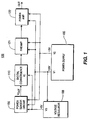
- Convergence system 100 includes a power supply 105, voltage regulator 108, power sensor circuit 150, digital convergence IC 110, preamp 121, and power amp 122.
- power sensor circuit 150 is utilized to enable digital convergence IC 110 only when the relevant supply voltages are being supplied at appropriate levels.
- Digital convergence IC 110 generates a correction signal, which is used to correct for vertical pincushion distortion and other distortions, as described above.
- the correction signal is conditioned by preamp 121 to provide a filtered or processed correction signal, which is then amplified by power amp 122, to provide an amplified output correction signal voltage at the pin marked "OUT".
- This amplified output voltage wave form is applied to a convergence yoke coil of a CRT unit (not shown).
- Power supply 105 provides supply voltages V1 and V2, which have nominal magnitudes of +15V and -15V, respectively, during normal operation.
- Voltages V1 and V2 are provided to preamp 121 and power amp 122 to provide power supplies for these devices.
- Voltages V1 and V2 are also applied as inputs to power sensor circuit 150.
- Voltage V1 is further applied as an input voltage to voltage regulator 108, which uses voltage V1 to derive an output voltage V3 having a magnitude of approximately +5V.
- Voltage V3 is coupled to digital convergence IC 110 to power the IC 110, and also to power sensor circuit 150.
- Output voltage V out of power sensor circuit 150 is coupled at its output terminal to an enable input terminal of digital convergence IC 110.
- voltage V1 is above a respective predetermined threshold and voltage V2 is below a predetermined threshold.
- these thresholds are nominally +12V and -12V, respectively.
- the actual values of the predetermined thresholds may be varied in accordance with circuit, signal, and load requirements.
- the normal range of voltage V1 in this embodiment is thus any voltage above approximately +12V, typically between approximately +12V and approximately +15V.
- the normal range of voltage V2 is any voltage below (i.e., greater in magnitude than) approximately -12V, typically between approximately -12V and approximately 15V.
- power sensor circuit 150 provides an output voltage V out of approximately +2.5V to the enable input terminal of IC 110.
- Digital convergence IC 110 is configured with comparator circuitry (not shown) coupled to its enable input terminal to monitor the V out signal from power sensor circuit 150 so that digital convergence IC 110 shuts down if V out falls below a predetermined minimum voltage, for example approximately +1.5V.
- IC 110 is configured so that IC 110 is enabled as long as Vout is within approximately 2.5V ⁇ 1V. Thus, as long as V out is within the range between approximately +1.5V and approximately +3.5V, IC 110 is enabled.
- IC 110 When IC 110 is enabled, it provides a correction signal to preamp 121 in the form of currents to preamp 121.
- Preamp 121 provides for low-pass filtering and differential amplification of the input correction signal currents, and provides an output voltage signal to power amp 122.
- V out is changed from approximately +2.5V to approximately 0V, thereby causing IC 110 to shut down when it senses that V out is less than approximately +1.5V.
- IC 110 shuts down by disabling the current sources of IC 110 that provide the correction signal current to preamp 121, for example by switching output currents to zero while maintaining a high impedance.
- IC 110 also shuts down by muting the output of preamp 121 by switching the output of preamp 121 to ground, so that preamp 121 does not provide an output voltage to power amp 122.
- a DC component is carefully limited as part of the signal applied to power amp 122 during normal operation, but could become unlimited if the input supply voltage V3 applied to IC 110 is disturbed while IC 110 is enabled.
- voltage V1 falls below its threshold of approximately +12V, causing voltage V out to fall from approximately +2.5V to approximately 0V, which in turn causes IC 110 to shut down.
- voltage V3 will still have a magnitude of approximately +5V for a short time, since voltage regulator 108 allows for a considerable amount of variation in the input voltage V1 before the output voltage V3 is affected.
- voltage V3 remains a t approximately +5V until voltage V1 drops below approximately +10V.
- IC 110 is thus shut down before voltage V3 begins to fall, thereby preventing the aforementioned problem that can arise when voltage V3, which is applied to IC 110, is disturbed before IC 110 is shut down.
- voltages V1, V2, and V3 are initially approximately 0V, and consequently V out equals approximately 0V. Voltages V1 and V2 begin to ramp up in magnitude, towards +15V and -15V, respectively. Until voltage V1 is approximately +8V, voltage V3 equals 0V. When voltage V 1 reaches approximately +8V, voltage regulator 108 has reached a sufficient input voltage to derive an output, and voltage V3 increases from approximately 0V to approximately +5V. When voltages V1 and V2 reach their respective threshold voltages of approximately +12V and approximately -12V, a delay of approximately 5 milliseconds is initiated. After the delay of 5 ms, V out switches from approximately 0V to approximately +2.5V. Thus, during start up, or after IC 110 has been disabled by V out switching to 0V, there is an approximately 5 ms delay after all three voltages V1, V2, and V3 have reached their respective threshold voltages, before IC 110 is enabled.
- This delay prevents IC 110 from erroneously being enabled when noise in convergence system 100 could momentarily cause each voltage V1, V2, V3 to exceed its threshold.
- the delay also helps to keep IC 110 from successively being enabled and disabled if one or more of voltages V1 or V2 is hovering around its respective threshold voltage.
- Circuit 150 is coupled at input terminals 151, 152, and 153 to input voltages V1, V2, and V3, respectively, as also illustrated in Fig. 1.
- Circuit 150 provides an output enable voltage V out at output terminal 155, which is coupled to the enable input of digital convergence IC 110.
- Input terminal 151 of circuit 150 is coupled through resistor R15 to terminals of resistors R13 and R16.
- the other terminal of resistor R13 is coupled to ground, and the other terminal of resistor R16 is coupled to a terminal of resistor R31 and to the base of pnp transistor Q18.
- Input terminal 152 is coupled through resistor R19 to a terminal of resistor R18 and to the base of npn transistor Q19.
- the emitter of transistor Q19 is coupled to ground, and the collector of transistor Q19 is coupled, through resistor R31, to the base of transistor Q18.
- Input terminal 153 is coupled through resistor R18 to the junction of the base of transistor Q19 and resistor R19, to the emitter of transistor Q18, to a terminal of capacitor C42, and to a terminal of resistor R11C, which is a component of IC 110.
- the collector of transistor Q18 is coupled through resistor R70 to the junction of the cathode of diode D3 and terminals of capacitor C42 and resistor R75.
- the anode of diode D3 is coupled to ground, and the other terminal of resistor R75 is coupled to the junction of the base of transistor Q5 and terminals of capacitor C44 and resistor R76, the other terminals of which are coupled to ground.
- the emitter of transistor Q5 is also coupled to ground, and the collector of transistor Q5 is coupled at output terminal 155 to the enable input of digital convergence IC 110, and also to the junction of resistors R11C and R21C of IC 110.
- the other terminal of resistor R21C is coupled to ground.
- Transistor Q19 is preferably of type MPSA20; transistor Q18 is of type MPSA55; and transistor Q5 is of type MPSA20.
- Diode D3 is of type dln4148.
- Resistors R11C, R21C of IC 110 each have a value of 10 K ⁇ .
- Voltage regulator 108 of convergence system 100 is a type 7805 voltage regulator, and power supply 105 is a switch mode power supply.
- power sensor circuit 150 is configured to perform the above-described functions. During normal operation, in power sensor circuit 150, since voltage V3 is derived from a voltage regulator, it is typically a relatively constant +5V during the time when either voltage V1 or voltage V2 would begin to drop out of a normal range and approach their thresholds. Voltage V3 is therefore used as a reference by circuit 150, against which voltages V1 and V2 are measured.
- resistors R18 and R19 form a voltage divider network that divides voltage V2 and compares it to the +5V reference voltage V3. If voltage V2 drops out of its normal range by reaching its threshold voltage of approximately -12V, the voltage at the base of transistor Q19 causes transistor Q19 to turn on, which thus causes transistor Q18 to turn on. As explained previously, turning transistor Q18 on ultimately causes IC 110 to be disabled. Even if a drop in voltage V2 does not imply a drop in voltage V1 and, therefore, in voltage V3 (which is derived from voltage V1), it is still advantageous to shut down IC 110 if voltage V2 falls below its threshold, since this could cause damage to power amp 122 or other components of convergence system 100.
- capacitor C42 performs the above-described delay function. As described above, voltages V1 and V2 begin to ramp up in magnitude, towards +15V and -15V, respectively. Until voltage V1 reaches approximately +8V, voltage V3 equals approximately 0V. When voltage V1 is approximately +8V, voltage V3 quickly increases from approximately 0V to approximately +5V. Transistor Q5 then immediately turns on since, at this point, capacitor C42 has not been charged. However, transistor Q18 is still on at this point, since voltages V1 and V2 have not yet reached their respective threshold voltages of approximately +12V and approximately -12V.
- transistor Q18 since transistor Q18 is still on, this keeps capacitor C42 shorted, thereby keeping it in a discharged state, and thus transistor Q5 stays on.
- voltages V1 and V2 reach their respective threshold voltages of approximately +12V and approximately -12V, transistors Q18 and Q19 both turn off.
- capacitor C42 begins charging and the voltage potential at the terminal of capacitor C42 coupled to diode D3 tends toward ground from approximately +5V.
- the terminal of capacitor C42 coupled to the cathode of diode D3 takes approximately 5 ms to drop from a potential of approximately +5V to approximately +1.2V, at which point transistor Q5 will turn off.
- V out switches from approximately 0V to approximately +2.5V.
Landscapes
- Engineering & Computer Science (AREA)
- Multimedia (AREA)
- Signal Processing (AREA)
- Video Image Reproduction Devices For Color Tv Systems (AREA)
- Amplifiers (AREA)
- Indication And Recording Devices For Special Purposes And Tariff Metering Devices (AREA)
Description
Claims (9)
- A convergence system (100) for a television receiver, said convergence system comprising:a convergence correction circuit (110) for providing a convergence correction signal current,a preamplifier (121) for receiving said convergence correction signal current, characterized in that said convergence system (100) comprises furthera power sensor circuit (150) being coupled to said convergence correction circuit (110) and to said preamplifier (121) for monitoring a power supply voltage (V1, V2, V3) provided to said convergence system (100),said power sensor circuit (150) disabling operation of output current sources of said convergence correction circuit (110), thereby providing zero correction signal currents to said preamplifier (121) and maintaining a high impedance of said convergence correction circuit (110), when the magnitude of said power supply voltage (V1, V2, V3) fulls below a threshold voltage level, and said power sensor circuit (150) enabling operation of the output current sources of said convergence correction circuit (110) thereby providing non-zero correction signal currents to said preamplifier (121) when the magnitude is at or above said threshold voltage level.
- The convergence system of claim 1, wherein said convergence system comprises further a voltage regulator (108) for deriving a derived supply voltage (V3) from said power supply voltage (V1), the magnitude of said derived supply voltage (V3) being less than the magnitude of said power supply voltage (V1), said derived supply voltage (V3) being coupled to said power sensor circuit (150) and to said convergence correction circuit (110),
- The convergence system of claim 2, wherein said power sensor circuit (150) uses said derived supply voltage (V3) as a reference voltage, against which a second and a third power supply voltage (V1, V2) are measured.
- The convergence system of claim 1, wherein said convergence system further comprises a power amplifier (122) for receiving and amplifying convergence correction signal provided by said preamplifier (121), said power amplifier having means for receiving said power supply voltage (V1, V2) to provide power to said power amplifier.
- The convergence system of claim 1,
wherein said power sensor circuit (150) comprises
an input for a connection to an input voltage potential (V1, V2);
a source of reference voltage potential;
a first transistor (Q18) having a control electrode coupled to said input voltage potential, a second electrode of said transistor (Q18) coupled to said source of reference voltage potential, and
delay means responsive to a conductive state of said transistor (Q18) for providing said output signal to said convergence circuit (110) a predetermined time after a change in said conductive state of said transistor (Q18) so to keep said convergence circuit (11c) disabled during said predetermined time and enable said convergence circuit after said predetermined time. - The convergence system of claim 5, wherein said first transistor changes from a conductive state to a non-conductive state when said input voltage potential exceeds a first predetermined threshold level.
- The convergence system of claim 6, wherein said delay means comprises a capacitor (C42) having first and second terminals coupled; respectively to said second electrode and a third electrode of said transistor (Q18).
- The convergence system of claim 7, wherein said output signal is enabled when a voltage at said second terminal of said capacitor falls below a second predetermined threshold voltage.
- A projection television cathode ray tube (CRT) system, comprising a convergence system (100) according to one of the preceding claims.
Applications Claiming Priority (3)
| Application Number | Priority Date | Filing Date | Title |
|---|---|---|---|
| US821189 | 1997-03-19 | ||
| US08/821,189 US5949499A (en) | 1997-03-19 | 1997-03-19 | Power sensor circuit for a conference system |
| PCT/US1998/004708 WO1998042141A1 (en) | 1997-03-19 | 1998-03-11 | Power sensor circuit |
Publications (2)
| Publication Number | Publication Date |
|---|---|
| EP0968614A1 EP0968614A1 (en) | 2000-01-05 |
| EP0968614B1 true EP0968614B1 (en) | 2003-06-11 |
Family
ID=25232756
Family Applications (1)
| Application Number | Title | Priority Date | Filing Date |
|---|---|---|---|
| EP98911557A Expired - Lifetime EP0968614B1 (en) | 1997-03-19 | 1998-03-11 | Convergence correction system with power sensor circuit |
Country Status (9)
| Country | Link |
|---|---|
| US (1) | US5949499A (en) |
| EP (1) | EP0968614B1 (en) |
| JP (1) | JP4100716B2 (en) |
| KR (1) | KR100521113B1 (en) |
| CN (2) | CN101072315A (en) |
| AU (1) | AU6548998A (en) |
| DE (1) | DE69815512T2 (en) |
| MY (1) | MY115577A (en) |
| WO (1) | WO1998042141A1 (en) |
Families Citing this family (4)
| Publication number | Priority date | Publication date | Assignee | Title |
|---|---|---|---|---|
| US6874683B2 (en) * | 1999-10-08 | 2005-04-05 | Canon Kabushiki Kaisha | User programmable smart card interface system for an image album |
| EP1491075A4 (en) * | 2002-04-04 | 2007-02-14 | Thomson Licensing | PROTECTION SYSTEM FOR POWER SUPPLY |
| CN101097249B (en) * | 2006-06-27 | 2011-08-10 | 中兴通讯股份有限公司 | Device used for low voltage electric power detection indicating |
| TW202410000A (en) * | 2022-05-09 | 2024-03-01 | 日商索尼集團公司 | Display system and operation method for display system |
Family Cites Families (8)
| Publication number | Priority date | Publication date | Assignee | Title |
|---|---|---|---|---|
| US4042858A (en) * | 1976-07-08 | 1977-08-16 | Gte Sylvania Incorporated | Television receiver protection circuit |
| US4197558A (en) * | 1978-02-16 | 1980-04-08 | Rca Corporation | Overload protection circuit for video amplifiers |
| JPH0543586Y2 (en) * | 1986-08-20 | 1993-11-02 | ||
| US4716463A (en) * | 1986-10-24 | 1987-12-29 | Zenith Electronics Corporation | Power down sense circuit |
| GB9109595D0 (en) * | 1991-05-02 | 1991-06-26 | Thomson Consumer Electronics | Polling for detection of power supply or other failures of a digital circuit |
| JPH05168025A (en) * | 1991-12-16 | 1993-07-02 | Sanyo Electric Co Ltd | Convergence drift correcting device |
| DE69325277T2 (en) * | 1993-12-31 | 2000-01-20 | Stmicroelectronics S.R.L., Agrate Brianza | Circuit for detecting a drop in supply voltage |
| DE19535868A1 (en) * | 1995-09-27 | 1997-04-03 | Thomson Brandt Gmbh | Circuit for the power supply of several power amplifiers |
-
1997
- 1997-03-19 US US08/821,189 patent/US5949499A/en not_active Expired - Fee Related
-
1998
- 1998-03-11 AU AU65489/98A patent/AU6548998A/en not_active Abandoned
- 1998-03-11 CN CNA200710096892XA patent/CN101072315A/en active Pending
- 1998-03-11 JP JP54059298A patent/JP4100716B2/en not_active Expired - Fee Related
- 1998-03-11 WO PCT/US1998/004708 patent/WO1998042141A1/en not_active Ceased
- 1998-03-11 CN CNB988035294A patent/CN100409694C/en not_active Expired - Fee Related
- 1998-03-11 DE DE69815512T patent/DE69815512T2/en not_active Expired - Fee Related
- 1998-03-11 EP EP98911557A patent/EP0968614B1/en not_active Expired - Lifetime
- 1998-03-11 KR KR10-1999-7008468A patent/KR100521113B1/en not_active Expired - Fee Related
- 1998-03-19 MY MYPI98001202A patent/MY115577A/en unknown
Non-Patent Citations (5)
| Title |
|---|
| ALLEN C.: "Analog Supervisor Chip Keeps Microprocessor out of Trouble", ELECTRONIC DESIGN, 30 April 1987 (1987-04-30), USA, pages 105 - 108 * |
| Data Sheet of Dallas Semiconductors DS1231, Pages 212 to 222 * |
| Data Sheet of Dallas Semiconductors DS1259, Pages 223 to 229 * |
| RS Components Data Sheet for RS3543 Power Supply Supervisor, July 1984 * |
| STRAHM M.: "Applications of a Swiss-made Watchdog", ELECTRONIC PRODUCT DESIGN, September 1987 (1987-09-01), pages 57 - 58 * |
Also Published As
| Publication number | Publication date |
|---|---|
| DE69815512T2 (en) | 2004-02-12 |
| MY115577A (en) | 2003-07-31 |
| KR100521113B1 (en) | 2005-10-14 |
| CN101072315A (en) | 2007-11-14 |
| US5949499A (en) | 1999-09-07 |
| KR20000076366A (en) | 2000-12-26 |
| WO1998042141A1 (en) | 1998-09-24 |
| JP4100716B2 (en) | 2008-06-11 |
| EP0968614A1 (en) | 2000-01-05 |
| AU6548998A (en) | 1998-10-12 |
| DE69815512D1 (en) | 2003-07-17 |
| JP2001516538A (en) | 2001-09-25 |
| CN1251242A (en) | 2000-04-19 |
| CN100409694C (en) | 2008-08-06 |
Similar Documents
| Publication | Publication Date | Title |
|---|---|---|
| CA1138100A (en) | Automatic kinescope biasing system | |
| US4042858A (en) | Television receiver protection circuit | |
| US4137552A (en) | Automatic beam current limiter with independently determined threshold level and dynamic control range | |
| CA1063712A (en) | Amplifier suitable for use as a color kinescope driver | |
| CA1257382A (en) | Television receiver with delayed display | |
| EP0968614B1 (en) | Convergence correction system with power sensor circuit | |
| CA1199103A (en) | Kinescope black level current sensing apparatus | |
| US6285401B1 (en) | Apparatus for suppressing overshoots in kinescope beam current measurement pulses | |
| KR920003724B1 (en) | Automatic Image Tube Bias Control | |
| US5410222A (en) | Sample pulse generator for automatic kinescope bias system | |
| KR100307572B1 (en) | Automatic kinescope bias device to prevent hot start flash | |
| JPS5820511B2 (en) | Color signal processing device | |
| KR910006459B1 (en) | Signal sampling device | |
| HK1111843A (en) | Power sensor circuit | |
| KR100465919B1 (en) | Display driver apparatus | |
| MXPA99008532A (en) | Power sensor circuit | |
| JP3077067B2 (en) | Television receiver | |
| MXPA04009648A (en) | Power supply protection arrangement. | |
| KR810001367B1 (en) | Auto Beam Current Limiter | |
| US4484227A (en) | Automatic kinescope bias control system compensated for sense point impedance variations | |
| JPH05505713A (en) | Beam current limiting configuration with threshold responsive to peak amplitude | |
| JPH02196289A (en) | Horizontal deflecting circuit | |
| JPH04373389A (en) | Transistor circuit for amplifying | |
| EP1001620A2 (en) | Apparatus for suppressing overshoots in kinescope beam current measurement pulses | |
| MXPA99010437A (en) | Apparatus to delete overmodulations in pulses of measure of beam current of cinesco |
Legal Events
| Date | Code | Title | Description |
|---|---|---|---|
| PUAI | Public reference made under article 153(3) epc to a published international application that has entered the european phase |
Free format text: ORIGINAL CODE: 0009012 |
|
| 17P | Request for examination filed |
Effective date: 19990910 |
|
| AK | Designated contracting states |
Kind code of ref document: A1 Designated state(s): DE GB |
|
| 17Q | First examination report despatched |
Effective date: 20000731 |
|
| GRAH | Despatch of communication of intention to grant a patent |
Free format text: ORIGINAL CODE: EPIDOS IGRA |
|
| RTI1 | Title (correction) |
Free format text: CONVERGENCE CORRECTION SYSTEM WITH POWER SENSOR CIRCUIT |
|
| GRAH | Despatch of communication of intention to grant a patent |
Free format text: ORIGINAL CODE: EPIDOS IGRA |
|
| GRAA | (expected) grant |
Free format text: ORIGINAL CODE: 0009210 |
|
| AK | Designated contracting states |
Designated state(s): DE GB |
|
| REG | Reference to a national code |
Ref country code: GB Ref legal event code: FG4D |
|
| REG | Reference to a national code |
Ref country code: GB Ref legal event code: 746 Effective date: 20030624 |
|
| REF | Corresponds to: |
Ref document number: 69815512 Country of ref document: DE Date of ref document: 20030717 Kind code of ref document: P |
|
| PLBE | No opposition filed within time limit |
Free format text: ORIGINAL CODE: 0009261 |
|
| STAA | Information on the status of an ep patent application or granted ep patent |
Free format text: STATUS: NO OPPOSITION FILED WITHIN TIME LIMIT |
|
| 26N | No opposition filed |
Effective date: 20040312 |
|
| PGFP | Annual fee paid to national office [announced via postgrant information from national office to epo] |
Ref country code: GB Payment date: 20080228 Year of fee payment: 11 |
|
| PGFP | Annual fee paid to national office [announced via postgrant information from national office to epo] |
Ref country code: DE Payment date: 20080319 Year of fee payment: 11 |
|
| GBPC | Gb: european patent ceased through non-payment of renewal fee |
Effective date: 20090311 |
|
| PG25 | Lapsed in a contracting state [announced via postgrant information from national office to epo] |
Ref country code: DE Free format text: LAPSE BECAUSE OF NON-PAYMENT OF DUE FEES Effective date: 20091001 |
|
| PG25 | Lapsed in a contracting state [announced via postgrant information from national office to epo] |
Ref country code: GB Free format text: LAPSE BECAUSE OF NON-PAYMENT OF DUE FEES Effective date: 20090311 |