EP0967838A1 - Thin film heating assemblies - Google Patents
Thin film heating assemblies Download PDFInfo
- Publication number
- EP0967838A1 EP0967838A1 EP98111684A EP98111684A EP0967838A1 EP 0967838 A1 EP0967838 A1 EP 0967838A1 EP 98111684 A EP98111684 A EP 98111684A EP 98111684 A EP98111684 A EP 98111684A EP 0967838 A1 EP0967838 A1 EP 0967838A1
- Authority
- EP
- European Patent Office
- Prior art keywords
- assembly
- substrate
- face
- resistive film
- heating
- Prior art date
- Legal status (The legal status is an assumption and is not a legal conclusion. Google has not performed a legal analysis and makes no representation as to the accuracy of the status listed.)
- Granted
Links
Images


Classifications
-
- H—ELECTRICITY
- H05—ELECTRIC TECHNIQUES NOT OTHERWISE PROVIDED FOR
- H05B—ELECTRIC HEATING; ELECTRIC LIGHT SOURCES NOT OTHERWISE PROVIDED FOR; CIRCUIT ARRANGEMENTS FOR ELECTRIC LIGHT SOURCES, IN GENERAL
- H05B3/00—Ohmic-resistance heating
- H05B3/20—Heating elements having extended surface area substantially in a two-dimensional plane, e.g. plate-heater
- H05B3/22—Heating elements having extended surface area substantially in a two-dimensional plane, e.g. plate-heater non-flexible
- H05B3/26—Heating elements having extended surface area substantially in a two-dimensional plane, e.g. plate-heater non-flexible heating conductor mounted on insulating base
- H05B3/265—Heating elements having extended surface area substantially in a two-dimensional plane, e.g. plate-heater non-flexible heating conductor mounted on insulating base the insulating base being an inorganic material, e.g. ceramic
-
- H—ELECTRICITY
- H05—ELECTRIC TECHNIQUES NOT OTHERWISE PROVIDED FOR
- H05B—ELECTRIC HEATING; ELECTRIC LIGHT SOURCES NOT OTHERWISE PROVIDED FOR; CIRCUIT ARRANGEMENTS FOR ELECTRIC LIGHT SOURCES, IN GENERAL
- H05B3/00—Ohmic-resistance heating
- H05B3/20—Heating elements having extended surface area substantially in a two-dimensional plane, e.g. plate-heater
- H05B3/22—Heating elements having extended surface area substantially in a two-dimensional plane, e.g. plate-heater non-flexible
- H05B3/26—Heating elements having extended surface area substantially in a two-dimensional plane, e.g. plate-heater non-flexible heating conductor mounted on insulating base
- H05B3/262—Heating elements having extended surface area substantially in a two-dimensional plane, e.g. plate-heater non-flexible heating conductor mounted on insulating base the insulating base being an insulated metal plate
-
- H—ELECTRICITY
- H05—ELECTRIC TECHNIQUES NOT OTHERWISE PROVIDED FOR
- H05B—ELECTRIC HEATING; ELECTRIC LIGHT SOURCES NOT OTHERWISE PROVIDED FOR; CIRCUIT ARRANGEMENTS FOR ELECTRIC LIGHT SOURCES, IN GENERAL
- H05B3/00—Ohmic-resistance heating
- H05B3/68—Heating arrangements specially adapted for cooking plates or analogous hot-plates
- H05B3/74—Non-metallic plates, e.g. vitroceramic, ceramic or glassceramic hobs, also including power or control circuits
- H05B3/748—Resistive heating elements, i.e. heating elements exposed to the air, e.g. coil wire heater
-
- H—ELECTRICITY
- H05—ELECTRIC TECHNIQUES NOT OTHERWISE PROVIDED FOR
- H05B—ELECTRIC HEATING; ELECTRIC LIGHT SOURCES NOT OTHERWISE PROVIDED FOR; CIRCUIT ARRANGEMENTS FOR ELECTRIC LIGHT SOURCES, IN GENERAL
- H05B2203/00—Aspects relating to Ohmic resistive heating covered by group H05B3/00
- H05B2203/016—Heaters using particular connecting means
-
- H—ELECTRICITY
- H05—ELECTRIC TECHNIQUES NOT OTHERWISE PROVIDED FOR
- H05B—ELECTRIC HEATING; ELECTRIC LIGHT SOURCES NOT OTHERWISE PROVIDED FOR; CIRCUIT ARRANGEMENTS FOR ELECTRIC LIGHT SOURCES, IN GENERAL
- H05B2203/00—Aspects relating to Ohmic resistive heating covered by group H05B3/00
- H05B2203/02—Heaters using heating elements having a positive temperature coefficient
Definitions
- the present invention relates to electric heating assemblies comprising a thin resistive film.
- the present invention assembly finds wide application in cooking appliances and related devices.
- Film heating elements comprising a layer of an electrically conductive metal are known such as disclosed in U.S. Patent 2,564,709 to Mochel which is herein incorporated by reference. Such film heating elements have typically been used for defrosting circuits on vehicular window assemblies. Other types of film heating devices are known, such as those disclosed in U.S. Patent 4,536,645 to Mio et al., which is herein incorporated by reference.
- Film heating elements have not found acceptance within the appliance industry although several film devices have been disclosed such as in U.S. Patents 4,889,974 to Auding et al. and 4,298,789 to Eichelberger et al., both of which are herein incorporated by reference. This is believed to result from a lack of reliability and serviceability associated with most contemplated film heating elements. Thus, there is a need for an assembly utilizing a film heating element that is both reliable and serviceable. Furthermore, it would be desirable to provide a film heating assembly that could be readily adapted and utilized in a wide variety of appliance applications.
- a heating assembly comprising a planar substrate, a thin electrically resistive film disposed on the substrate, and a non-stick layer disposed on an opposite side of the substrate.
- the resistive film may comprise a metal oxide or doped metal oxide.
- the non-stick layer may comprise polytetrafluoroethylene.
- One or more electrically insulating layers can be disposed between the resistive film and the substrate or on the top side of the substrate.
- the heating assembly may also comprise electrically conductive electrodes in electrical association with the resistive film, the electrodes preferably comprising a cermet-based silver thick film material.
- the substrate may comprise porcelainized carbon steel, porcelainized ferritic stainless steel, aluminum oxide, glass ceramic designated under the trade name Ceran, Si 3 N 4 -ceramic, or combinations thereof.
- the present invention provides a warming assembly comprising a substrate such as for example an appliance cook top, a thin electrically resistive film in thermal association with the cook top, and at least two electrically conductive electrodes in electrical association with the resistive film.
- the appliance cook top may comprise a glass ceramic material.
- One or more layers of an electrically insulating adhesive material may be disposed around the resistive film.
- various clamping assemblies can be utilized for maintaining the resistive film in thermal association with the cook top.
- the warming assembly may further comprise an appliance mounting channel by which the warming assembly is supported.
- the present invention provides cooking appliances comprising the noted heating and warming assemblies.
- an appliance comprising a planar heating or warming assembly that provides a cooking surface, an enclosure for supporting and containing the assembly, and a controller for adjusting and maintaining the temperature of the assembly.
- an appliance is provided that comprises a glass ceramic cook top in conjunction with the noted heating or warming assemblies.
- an appliance is provided that utilizes one or more of the heating assemblies as heating panels disposed within an oven interior. The present invention also provides appliances utilizing the noted heating or warming assemblies in combination with conventional heating elements known in the art.
- the present invention provides heating and warming assemblies that utilize a thin electrically resistive film.
- the term “thin film” generally refers to films having a thickness from about 0.1 to about 1.0 micrometers.
- the term “heating assembly” generally refers to an assembly that is capable of providing a temperature of between about 200°C and about 350°C along its heating surface.
- the heating assemblies described herein may be designed and constructed so that they are operable at temperatures higher than 350°C, such as up to about 400°C.
- the term “warming assembly” as used herein generally refers to an assembly that is capable of providing a surface temperature between about 40°C and about 200°C along its heating surface.
- the preferred embodiment thin film heating assemblies of the present invention generally comprise (i) a substrate, (ii) a resistive film for heat generation in thermal association with the substrate, (iii) one or more electrically conductive electrodes or bus bars in electrical association with the resistive film, and (iv) a non-stick layer disposed on the exposed surface(s) of the assembly.
- the preferred embodiment thin film heating assemblies may further comprise (v) one or more dielectric or electrically insulating layers disposed on one or both sides of the resistive film (ii), or on the substrate side that is opposite the substrate side facing the resistive film. In some applications, it may also be preferred to provide an electrically conductive layer on the substrate side opposite the substrate side facing the resistive film. This is described in greater detail below.
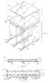
- FIG. 1 is an exploded view of a first preferred embodiment thin film heating assembly 110 in accordance with the present invention.
- the accompanying figures are not necessarily to scale.
- the thickness of the resistive film and other layers has been exaggerated to better illustrate the structure and relationship of the various components.
- the resistive film may be several orders of magnitude thinner than other components of the assemblies such as for instance the substrate. This aspect is described in greater detail below. Referring to FIG.
- assembly 110 comprises a substrate 120, one or more resistive films 130 disposed on one side of the substrate 120 and in thermal association with the substrate 120, one or more outer electrodes 140 that are in electrical association with the resistive films 130 and disposed on the same side of the substrate 120 as the resistive films 130, one or more inner electrodes 150 that are also in electrical association with the resistive films 130 and disposed on the same side of the substrate 120 as the resistive films 130 and the outer electrodes 140, and a non-stick layer 160 disposed on a side of the substrate 120 opposite the substrate side facing the resistive films 130 and the electrodes 140 and 150.
- the substrate 120 is preferably planar having a first or outer (upper) face 122, an oppositely directed second or inner (lower) face 124, and a peripheral edge 121.
- the substrate 120 is depicted in FIG. 1 as rectangular in shape, it is to be understood that the substrate 120 may have nearly any shape including circular, oval, and elliptical shapes.
- the thickness of the substrate 120 is generally dictated by the end use requirements for the assembly 110. Typical thicknesses for the substrate 120 range from about 0.5 millimeters up to about 1 centimeter. It is preferred that the thickness of the substrate 120 is generally uniform. Although it is generally preferred that the substrate 120 is flat, it is contemplated that one or both sides of the substrate could be curved or otherwise nonplanar.
- the substrate 120 is generally planar having one finished, relatively smooth face and a second dimpled face. This configuration is typical for substrates of glass ceramic, particularly those available under the designation Ceran.
- the smooth face of the substrate serves as the outer or upper face 122 and the dimpled face serves as the inner or lower face 124.
- the resistive films 130 each have a top surface 132 and a bottom surface 134. As noted, multiple resistive films 130 can be utilized in the present invention assemblies. It is preferred that all films 130 be disposed in the same plane. It is also preferred that the top surface 132 of each resistive film 130 be directed toward, and most preferably immediately adjacent and in contact with, the second face 124 of the substrate 120. The configuration promotes thermal conduction between the resistive films 130 and the substrate 120. It is also preferred that the entirety or at least a majority of the surface area of the second face 124 be covered by the resistive films 130. Accordingly, the collective shape resulting from the resistive films 130 is preferably similar to the shape of the substrate 120. The preferred thickness for the resistive films 130 is described below.
- the outer electrodes 140 and inner electrodes 150 are preferably straight or linear and oriented parallel with the plane of the substrate 120.
- the electrodes 140 and 150 are preferably thin strip-like elements having a length dimension significantly greater than their width dimension.
- the thickness of each electrode 140 and 150 is preferably from about 5 to about 25 micrometers.
- Each outer electrode 140 includes an electrical lead or termination 142, a top face 144, and a bottom face 146.
- Each inner electrode 150 includes an electrical lead or termination 152, a top face 154, and a bottom face 156.
- FIG. 1 illustrates the outer electrodes 140 as disposed alongside and adjacent an outer edge of the assembly 110, it is to be understood that one or more, or all of the outer electrodes 140 could be disposed near an intermediate region of the assembly 110.
- other configurations for the inner electrodes 150 and the combination of the inner electrodes 150 and the outer electrodes 140 are contemplated.
- the present invention includes a wide array of configurations and arrangements for the resistive film 130 and the electrodes 140 and 150.
- the electrodes 140 and 150 of an alternate assembly 112 can be disposed immediately adjacent the substrate 120, and the resistive film 130 disposed and overlying not only the substrate 120 but also the electrodes 140 and 150. Additional aspects of the preferred embodiment electrodes 140 and 150 are discussed below.
- the non-stick layer 160 includes an outwardly facing surface 162 and a second surface 164.
- the outwardly facing surface 162 preferably constitutes the exposed heating surface of the assembly 110.
- the second surface 164 is preferably disposed immediately adjacent and in contact with the first face 122 of the substrate 120.
- the assembly 110 is preferably powered by appropriate connection to an electrical power source, such as a three-wire 220 volt supply.
- Assembly 110 is connected to such a source by connecting the outer electrodes 140 to a respective hot line, e.g. H 1 or H 2 , and if desired, an inner electrode 150 can be connected to ground or neutral, e.g. N.
- the assembly 110 can also be appropriately connected to other three-wire systems, or to two-wire systems.
- FIG. 2 is a cross-sectional view of the first preferred embodiment thin film heating assembly 110 taken along line 2-2 shown in FIG. 1. As illustrated in FIG. 2, it is preferred that the resistive films 130 are disposed underneath and immediately adjacent the substrate 120. The resistive thin films 130 are electrically connected to the electrodes 140 and 150 by disposing the electrodes directly on top, or underneath, the thin films 130.
- FIG. 2A is a cross-sectional view of another preferred embodiment thin film heating assembly 118 in accordance with the present invention.
- the thin film heating assembly 118 comprises the previously described substrate 120, resistive films 130, one or more outer electrodes 140, one or more inner electrodes 150, and the non-stick layer 160.
- the assembly 118 further comprises a dielectric or electrically insulating layer 170 disposed between the substrate 120 and the layer of the resistive films 130.
- the electrically insulating layer 170 can be disposed on the bottom surface 134 of the resistive films 130.
- the electrically insulating layer 170 has a size and shape sufficient for it to cover, or substantially so, the components upon which it is disposed.
- the components upon which the electrically insulating layer 170 is disposed include the substrate 120, the resistive films 130, the outer electrodes 140, and the inner electrode 150.
- the electrically insulating layer 170 may be disposed on the substrate side opposite the substrate side facing the resistive film, i.e. side 122.
- the thickness of the electrically insulating layer 170 primarily depends upon the electrical insulation properties, i.e. the volume resistivity and dielectric constant, of the material forming the layer 170, and the electrical operating characteristics of the thin film heating assembly 118.
- the thickness of the layer 170 may also vary depending upon the particular application, but should in all cases, be sufficiently thick to prevent electrical current loss or short circuiting of the resistive films 130, the outer electrodes 140, and the inner electrodes 150. As described in greater detail below, it may in some applications be preferred to provide an electrically conductive layer on the outermost top surface of the assembly. This layer may be in addition to, or replace, the layer 170 when layer 170 is disposed on the substrate side opposite the substrate side facing the resistive film.
- the substrate (i) can be nearly any heat resistant, relatively rigid material.
- the material selected for the substrate (i) should also exhibit electrical insulating properties or be coated or otherwise treated to have such property.
- the material selected for the substrate (i) should have a relatively low coefficient of thermal expansion. Examples of materials suitable for use as the substrate (i) include, but are not limited to, porcelainized carbon steel, porcelainized ferritic stainless steel, aluminum oxide, glass ceramic commonly referred to as Ceran, Si 3 N 4 -ceramic, and combinations of the foregoing.
- a particularly preferred material for the substrate is glass ceramic.
- a preferred glass ceramic is Li 2 Al 2 Si 2 O 6 beta-quartz (LAS), such as available from Eurokera or Schott. If a porcelainized steel is selected for use as the substrate (i), it should be free of alkali and alkali earth metals so as to maintain good electrical insulating properties at temperatures above 150° C. A supplier of such porcelainized steel substrates is Ferro. Glass ceramic is generally preferred since as compared to other substrates, glass ceramic exhibits a relatively low thermal shear stress. The coefficient of thermal expansion of glass ceramic is essentially zero as compared to steel having a coefficient of thermal expansion of about 11 ppm. The use of near zero thermal expansion glass ceramic significantly reduces the tendency of crazing and cracking of other layers or films deposited on the glass substrate such as tin dioxide.
- LAS Li 2 Al 2 Si 2 O 6 beta-quartz
- the electrically resistive film (ii) can be a thin film of metal oxide such as for instance tin dioxide, a cermet-based thick film material, a polymer-based thick film material, or any type of electrically resistive film or coating. It is preferred that the resistive film (ii) is a thin film of metal oxide, and most preferred that the metal oxide thin film be a doped tin dioxide thin film. A preferred dopant for tin dioxide is 0.1 to 0.5 weight percent fluorine. It is also preferred that the metal oxide thin film be deposited on a face of the substrate (i) by an atmospheric chemical vapor deposition (ACVD) process.
- a preferred dopant for tin dioxide is 0.1 to 0.5 weight percent fluorine.
- the metal oxide thin film be deposited on a face of the substrate (i) by an atmospheric chemical vapor deposition (ACVD) process.
- ACCVD atmospheric chemical vapor deposition
- One preferred metal oxide for example is tin dioxide thin film doped with approximately 0.4 weight percent fluorine, and applied by an atmospheric chemical vapor deposition process at approximately 550°C. It is contemplated that other techniques for depositing the resistive film (ii) could be utilized. For instance, liquid materials or resistive film precursors could be applied by spraying and if necessary followed by additional spray coatings, exposure to heat or radiation, or other operations depending upon the end use application.
- the material utilized for forming the resistive film (ii) has a positive temperature coefficient (PTC) with respect to its electrical resistance.
- PTC positive temperature coefficient
- the temperature coefficient of resistance may be adjusted by adding appropriate amounts of oxides of iron, cobalt, nickel, niobium, tantalum, zirconium, and hafnium. It is important that the resistive film (ii) exhibit a PTC so that electrical resistance of the film increases with temperature. This property prevents temperature runaway during application of electrical power to the heating assembly. It is preferable to utilize a resistive film that has a linear PTC in the range of 25° to 400°C. Doped tin dioxide exhibits this property.
- the resistive film (ii) should be able to accommodate a power density of between about 1.0 to about 20 W/cm 2 and a current density of between about 11,000 to 90,000 A/cm 2 .
- the thickness of the resistive film (ii) varies depending upon the materials utilized for the resistive film (ii) and the particular application.
- the preferred thickness of such films generally ranges from about 0.1 to about 0.5 micrometers for most metal oxides or doped metal oxides, including tin dioxide.
- the thickness of the resistive film when formed from a thick-film material is between about 1 and about 25 micrometers.
- a tin dioxide thin film may be applied to the dimpled underside of a Ceran type glass ceramic substrate.
- a dimpled surface has a greater amount of surface area available for bonding than a relatively smooth surface. The increased surface area decreases the wattage or power density carried by the thin film and so, promotes reliability of the thin film.
- the dimpled surface also prevents or minimizes fractures of the substrate.
- a dimpled substrate have a particular configuration as follows.
- the dimpled surface preferably comprises a plurality of closely arranged dimples that project outward a distance of from about 40 to about 200 micrometers from the substrate surface.
- Each dimple is preferably oval shaped and oriented so that its major diameter is parallel with the longitudinal axis of the substrate. It is most preferred that all of the dimples, or at least a majority, be oriented parallel to one another and with the longitudinal axis of the substrate.
- the preferred major diameter for each oval is about 2.1 millimeters.
- the preferred minor diameter of each oval is about 1.75 millimeters.
- the ovals are preferably spaced from each other by about 3.4 millimeters between centerpoints of adjacent dimples as measured along their width or minor diameter, and about 2.5 millimeters between centerpoints of adjacent dimples as measured along their length or major diameter.
- the electrodes or bus bars (iii) are preferably formed from a cermet-based silver thick film material. It is contemplated that other electrically conductive materials could be utilized for the electrodes (iii). The selected materials should be compatible with other materials utilized in the resulting heating assembly.
- a preferred material for the electrodes is a silver cermet. This preferred material is applied by screen printing. In its printable state, it comprises a carrier or solvent, glass frit, and silver particles. When deposited on a glass substrate and fired at approximately 550°C, it forms a blend with the glass substrate as a continuous phase with the silver particles dispersed therein. Silver cermet materials are available from DuPont, ESL, and Ferro for example.
- the non-stick layer (iv) is preferably formed from crosslinked silicone or polytetrafluoroethylene (PTFE) impregnating a porous scratch resistant structure like flame sprayed stainless steel.
- PTFE polytetrafluoroethylene
- Various crosslinked silicone compositions may be utilized for the non-stick layer (iv).
- the optional dielectric layer (v) is preferably any electrically insulating material that is suitable for exposure to relatively high temperatures, such as generated by the heating assemblies described herein.
- materials include silicone dioxide, titanium dioxide, inorganic high temperature cements, sealing glasses, sol gel applied ceramics such as zirconia applied as a sol gel, high temperature paint, plasma or flame sprayed ceramics, or combinations thereof.
- the dielectric material selected preferably has a coefficient of thermal expansion as close to the substrate (i) as possible.
- a specific example of a preferred material for the dielectric layer is a glass layer fused to a glass ceramic substrate. Such fusing can be performed at temperatures in the range of 600°C to 850°C.
- a preferred material for the dielectric layer is a thin film of titanium dioxide TiO 2 . This can be applied via atmospheric chemical vapor deposition.
- a further specific example of a preferred material for the dielectric layer is a ceramic material, for instance an alumina-based ceramic material, that is plasma sprayed or HVOF sprayed.
- Another specific example of a preferred material is zirconium dioxide (ZrO 2 ) that is applied as a sol gel.
- the optional dielectric layer (v) can be incorporated into any of the heating or warming assemblies described herein. Multiple dielectric layers may be utilized where necessary.
- a preferred location for incorporating one or more electrically insulating layers in the assemblies described herein is between the electrically resistive film (ii) and the substrate (i) and on the upper substrate side.
- the present invention includes assemblies comprising a top or outermost layer of an electrically conductive material. It may in some applications, be desirable to provide an electrical connection between that top electrically conductive material and an electrical ground.
- a preferred material for this top electrically conductive grounding layer is ACVD fluorine doped tin dioxide (SnO 2 ) thin film having a thickness of from about 0.1 to about 0.5 micrometers, or an Invar-alloy film, for example Fe-Ni, having a thickness of from about 0.1 to about 10 micrometers.
- any or all of the electrode or bus bars (iii), the non-stick layer (iv), and/or the dielectric layer (v), and the optional safety ground layer can be formed by screen printing techniques, spray coating operations, or other suitable techniques depending upon the characteristics of the starting materials.
- the electrodes or bus bars (iii) are formed from an initially flowable material, such as thick film paste materials, it is preferred to screen print the electrode material directly onto the surface of interest. This enables formation of any desired arrangement or pattern of electrodes or bus bars in a simple and economical fashion.
- CTE coefficient of thermal expansion
- the substrate (i) preferably comprises a glass ceramic.
- the resistive film (ii) is preferably formed from doped ACVD tin dioxide.
- a cermet-based silver thick film is utilized for the electrodes or bus bars (iii).
- the non-stick layer (iv) consists of crosslinked silicone or PTFE impregnating a porous scratch resistant structure like flame sprayed stainless steel or plasma sprayed ceramic.
- Heating by the thin film heating assemblies, such as assembly 110 is performed by passing electrical current through the resistive film 130. This is preferably achieved by electrically connecting the electrical leads 142 to a voltage source.
- a controller can be used to regulate the flow of electric current to control the temperature of the resistive film or the heating assembly. If utilizing doped tin oxide for the resistive film (ii), the linear PTC characteristic of that material enables direct temperature control by monitoring the change in current versus temperature change.
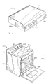
- FIG. 3 illustrates a griddle 200 comprising a thin film heating assembly 210, one or more controls 220, and an enclosure 230.
- the thin film heating assembly 210 is preferably similar to the previously described heating assemblies.
- the heating assembly 210 is incorporated within the enclosure 230 by techniques known to those skilled in the art.
- FIG. 4 illustrates a domestic range 300 comprising a plurality of thin film heating assemblies in accordance with the present invention.
- the range 300 comprises a planar, relatively large surface area griddle 310 utilizing a thin film heating assembly such as the previously described heating assembly 210.
- the range 300 may comprise one or more oven heating panels 330 disposed in the lower portion of the range 300 that employ the thin film heating assembly of the present invention. These oven heating panels 330 are described in greater detail below.
- the range 300 may utilize any combination of the griddle 310 and the oven heating panels 330.
- the range 300 may further comprise one or more heating element elements 348 in the form of conventional electrical resistance elements known in the art, or in accordance with the present invention thin film heating assemblies.
- the range 300 generally comprises an enclosure 340, a door 346 pivotally attached thereto, and indicators and electronic controls 342 and 344 respectively, for monitoring and controlling the operation of the griddle 310, the oven heating panels 330, and the heating element elements 348.
- the thin film heating assembly of the present invention is particularly well suited for use as an oven heating panel that can supplement and most preferably replace conventional oven baking elements.
- Replacing conventional oven baking elements with the heating assembly of the present invention provides an oven that is significantly easier to clean.
- the non-stick outer surface of a thin film heating assembly that is incorporated into an oven heating panel and elimination of conventional baking elements facilitate cleaning the oven after use.
- Replacement of conventional baking elements with a heating panel utilizing the thin film heating assembly increases the effective oven volume.
- replacement of conventional baking elements with a heating panel utilizing the thin film heating assembly results in energy savings and promotes temperature uniformity within the oven interior.
- the oven heating panels 330 can be disposed along any wall or portion thereof within the oven interior.
- one or more oven heating panels are disposed along the rear wall of the oven interior.
- one or more oven heating panels are located on the bottom wall of the oven interior, preferably replacing a conventional lower baking element.
- one or more oven heating panels are located on the top wall of the oven interior, preferably replacing a conventional upper heating element such as a broiling element. It is also contemplated to incorporate one or more heating panels on the inward facing surface of the oven door 346. All of the noted oven heating panels could be employed in any combination.
- the present invention includes a range or oven comprising a plurality of oven heating panels 330 disposed on any combination of surfaces defining the oven interior. It is also contemplated that a plurality of oven heating panels 330 may be located on a single wall or common surface of the oven interior. This may be desirable so that exposed noncovered portions of the underlying wall such as between spaced apart adjacent oven heating panels 330, can provide mounting or support provisions for oven racks, rotisserie components, lights, viewing windows, or other items.
- the shape of the oven heating panels is not critical.
- a range comprises a plurality of oven heating panels disposed in the lower portion of the oven interior. At least one of the oven heating panels is adapted to be selectively positioned to different locations within the oven interior, much like an oven rack may be placed at various locations within the oven interior.
- FIG. 4A illustrates an alternate preferred embodiment range 305 comprising one or more selectively positionable oven heating panels 332.
- the range 305 preferably comprises many of the same components as previously described with respect to the range 300 shown in FIG.
- the range 305 further comprises a selectively positionable oven heating panel 332 that can be placed at various locations within the oven interior.
- the range 305 will typically include one or more upper racks 320 disposed near the upper portion of the oven interior, and one or more lower racks 322 disposed near the lower portion of the oven interior.
- the interior side walls of the oven provide horizontally extending support ridges or ledges 324 for supporting an upper or lower oven rack 320 or 322, or a positionable oven heating panel 332.
- the selectively positionable oven heating panels 332 can be placed at any location within the interior of the oven provided sufficient supports are provided at the desired location such as a pair of support ridges 324. This feature of a selectively positionable heating panel provides significantly greater flexibility in heating or baking operations than with conventional ovens utilizing non-positionable heating elements.
- the positionable oven heating panel 332 may be moved to a new location within the oven interior, such as location 334 depicted in FIG. 4A by dashed lines, by sliding or otherwise removing the panel 332 outward from the oven interior, as one would remove an oven rack such as upper rack 320, and then placing the panel 332 at the new location, e.g. location 334, within the oven interior.
- a flexible cable housed within an appropriate flexible cover or conduit can be used to provide both electrical power and control signals to the panel 332.
- the flexible cable may extend from a rear wall of the oven interior to a rearwardly directed edge or the underside of the panel 332.
- a plurality of plug receptacles could be provided on one or more walls of the oven interior, and one or more corresponding mating receptacles provided on the panel 332 such that upon appropriate placement of the panel, such as between a pair of support ridges 324 and against the oven rear wall, the plugs are engaged thereby completing the requisite power and control circuits between the panel 332 and the range 305.
- the oven heating panel 330 or 332 comprises a thin film heating assembly generally corresponding to the previously described thin film heating assemblies, and further comprises a coating or layer of suitable material adapted for exposure to the oven interior.
- an oven heating panel 330 or 332 can be formed by utilizing a suitable oven interior coating material known in the art as the previously described non-stick layer (iv) in conjunction with any of the previously noted preferred embodiment thin film heating assemblies.
- the present invention also provides a warming assembly comprising a thin electrically resistive film.
- the warming assembly is particularly well suited for providing a warming zone on a cook top and preferably a smooth planar cook top such as used in modern ranges and cooking appliances.
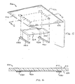
- FIG. 5 is a perspective view of the underside of a first preferred embodiment thin film warming assembly 400 in accordance with the present invention.
- the assembly 400 comprises a cook top 410, a thin electrically resistive film 420 disposed on the underside of the cook top 410, and one or more bus bars 430 in electrical association with the resistive film 420.
- the cook top 410 has a top heating surface 412 upon which is typically placed containers or food items to be heated or warmed, and a cook top underside 414.
- the cook top 410 is preferably a glass ceramic cook top as known in the art.
- the resistive film 420 corresponds to the thin film 130 of the previously described thin film heating assemblies.
- the resistive film 420 is preferably tin dioxide.
- the resistive film 420 has an upper surface 422 and a lower surface 424.
- the resistive film 420 is preferably deposited on the underside of the cook top 410 such that the upper surface 422 of the resistive film 420 is in contact with the cook top underside 414.
- the bus bars 430 correspond to the previously described electrodes 140 and 150.
- the bus bars 430 are preferably formed from a cermet-based thick film.
- Each bus bar 430 comprises a termination pad 432 at which external electrical connections to the bus bar 430 are established.
- FIG. 6 illustrates a cross-sectional view of the first preferred embodiment thin film warming assembly 400 shown in FIG. 5 taken along line 6-6. Again, it will be appreciated that the illustration is not necessarily to scale. It is to be understood that although FIGS. 5 and 6 depict the resistive film 420 in a stacked or overlying relationship with the bus bars 430, alternate configurations are included in the present invention.
- FIG. 7 is an exploded view of a second preferred embodiment of a thin film warming assembly 500 having such a configuration.
- the assembly 500 comprises a cook top 510 similar to the previously described cook top 410.
- the cook top 510 provides a top cooking, heating, or warming surface 512 and an underside surface 514.
- the assembly 500 further comprises a substrate 540 and a resistive film 520 deposited or otherwise disposed thereon.
- the substrate 540 corresponds to the previously described substrate 120, and provides a first face 542 and a second face 544.
- the resistive film 520 corresponds to the previously described resistive film 130, and includes an upper surface 522 and a lower surface 524.
- the assembly 500 further comprises an adhesive layer 550 disposed between the cook top 510 and the resistive film 520 for securing and maintaining those components in heat transfer relationship with each other.
- the adhesive layer 550 includes a top surface 552 and a bottom surface 554. Most preferably, the adhesive layer 550 is disposed between the underside 514 of the cook top 510 and the upper surface 522 of the resistive film 520.
- the adhesive layer 550 can be formed from nearly any adhesive suitable for the end use conditions for the assembly 500.
- the adhesive used for the adhesive layer 550 is a heat conductive, heat resistant, two component silicone elastomer.
- the adhesive layer 550 is electrically insulating.
- the assembly 500 also comprises one or more bus bars 530 in electrical association with the resistive film 520.
- the bus bars 530 each provide a termination area 532 and correspond to the previously described electrodes 140 and 150.
- the bus bars 530 are preferably disposed alongside or adjacent two opposite edges of the resistive film 520 as shown in FIG. 7.
- Other affixment techniques besides the use of adhesives could be employed for securing the resistive film 520 to the cook top 510. It will be appreciated that although FIG. 7 illustrates the resistive film 520 in a stacked or overlying relationsh-ip with the bus bars 530, alternate configurations are included in the present invention.
- FIG. 7A is a detailed exploded view of a preferred end connection at a bus bar 530 of the assembly 500 shown in FIG. 7.
- the bus bar 530 comprises an inclined segment 534 extending between the bus bar termination 532 and the major portion of the bus bar 530.
- the inclined segment 534 is angled away from the underside 514 of the cook top 510 so as to provide a clearance space between the bus bar 530 and the underside 514 of the cook top 510.
- One or more electrical leads 570 are connected to the bus bar 530 and specifically to the bus bar termination 532 by a threaded fastener 574 and nut 576.
- an electrically insulating end cap 578 is preferably disposed over the end of the fastener 574.
- the end cap 578 can be formed from nearly any electrically insulating flexible material. A heat resistant silicone rubber tubing has been found useful for the end cap 578.
- FIG. 7A it is also within the scope of the invention to utilize a rivet connection between an electrical lead, such as lead 570 in FIG. 7A, and the bus bar termination 532. It is also contemplated that the bus bar or electrode could be disposed immediately adjacent to the substrate or cook top instead of being spaced therefrom as shown in FIG. 7A. An aperture is then preferably provided at the location for attachment of an electrical lead, and a fastener or rivet inserted therethrough. An electrically insulating washer or fastener can be used at the point of attachment between the electrical lead and bus bar, so that the portion of the fastener or rivet on the opposite side of the substrate is electrically isolated from the electrical lead and bus bar.
- the present invention includes additional coupling assemblies for providing electrical connection between the thin film heating or warming assembly and the appliance, or at least the power supply leads.
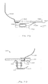
- a second preferred embodiment electrical coupling assembly 1000 is illustrated in FIGS. 7B and 7C.
- the second preferred embodiment electrical coupling assembly 1000 comprises a receptacle 1010 affixed to a heating or warming assembly as described herein.
- FIGS. 7B and 7C illustrate the electrical coupling assembly 1000 affixed to a substrate 1040, and in electrical association with a resistive film 1050.
- the receptacle 1010 may be a conventional female plug coupler as known in the art and available from Amp.
- the receptacle 1010 provides a receiving chamber 1012 for releasably engaging a corresponding male connector.
- the receptacle 1010 comprises one or more electrical conductors 1030 accessible from the receiving chamber 1012.
- the conductors 1030 extend to, or are in electrical association with, a corresponding number of bus bars 1032, such as disposed on the underside of the resistive film 1050.
- the electrical conductors 1030 are preferably electrically connected to the respective bus bars 1032 at a corresponding number of termination regions 1034. All electrical connections between the conductors 1030 and the bus bar termination regions 1034 are preferably achieved by soldering.
- the connector assembly 1000 is utilized to selectively establish electrical connections between the heating or warming assembly and the appliance or product enclosure. The electrical connections may be for power supply connections or for control signal or electrical measurement connections.
- FIG. 7B also illustrates a mounting configuration for a heating or warming assembly of the present invention.
- One or more enclosure panels 1060 such as constituting an appliance enclosure may be formed to provide a generally horizontal lip 1062 upon which the heating or warming assembly is mounted and affixed.
- the previously described receptacle 1010 can be affixed to the enclosure panel 1060.
- Other techniques for mounting a heating or warming assembly within an enclosure can be utilized including for instance threaded fasteners and rivets.
- FIG. 7D A third preferred embodiment electrical coupling assembly 1100 is illustrated in FIG. 7D.
- This third preferred embodiment coupling assembly 1100 comprises a dual prong union member 1110 having a first projection 1112 and a second projection 1114, both projections for establishing electrical connection therebetween.
- the union member 1110 further has a resilient mounting member 1120 adapted for affixment to an enclosure panel 1130 or an enclosure mounting frame 1132.
- the union member 1110 is attached to a heating or warming assembly described herein, preferably by welding or brazing the mounting member 1120 to a peripheral edge or lip of the enclosure panel 1130 or to a region of the enclosure mounting frame 1132.
- the mounting member 1120 may be affixed to a heating or warming assembly by mechanical fasteners such as rivets 1134 shown in FIG. 7D.
- the second projection 1114 should contact a termination region of a bus bar or other electrical component. Accordingly, electrical connection to the bus bar at the second projection 1114 is made at the first projection 1112.
- the coupling assemblies described herein are exemplary, and the present invention heating and warming assemblies may utilize nearly any type of electrical connector to establish power, signal, or other electrical current flows to and from the heating or warming assembly.
- FIG. 8 is an exploded view of a third preferred embodiment thin film warming assembly 600 in accordance with the present invention.
- the assembly 600 comprises a cook top 610 similar to the previously described cook top 410.
- the cook top 610 provides a top cooking, heating, or warming surface 612 and an underside surface 614.
- the assembly 600 further comprises a substrate 640 and a resistive film 620 deposited or disposed thereon.
- the substrate 640 is similar to the previously described substrate 120, and provides a first face 642 and a second face 644.
- the resistive film 620 corresponds to the previously described resistive film 130, and includes an upper surface 622 and a lower surface 624.
- the assembly 600 further comprises bus bars 630 which correspond to the previously described electrodes 140 and 150.
- the bus bars 630 are disposed on the side of the film 620 opposite the cook top 610.
- the bus bars 630 are preferably disposed proximate to the opposite edges of the resistive film 620.
- the termination ends 632 of the bus bars 630 may also be configured as the configuration depicted in FIG. 7A. Alternatively or in addition, electrical connections can be established by the assemblies shown in FIGS. 7B-7D.
- the substrate 640 and resistive film 620 are affixed to and placed in thermal association with the cook top 610 by one or more clamps 660.
- the clamps 660 enable the assembly of substrate 640, the resistive film 620, and the bus bars 630 to be releasably engaged with the cook top 610.
- each clamp 660 is preferably affixed to the underside 614 of the cook top 610 by an effective amount of an adhesive 670.
- the adhesive 670 is preferably a single component heat resistant silicone elastomer known to those skilled in the art.
- the thin film warming assembly 600 includes variant embodiments in which one or more clamps 660 are affixed to the cook top 610 by mechanical fasteners or other techniques besides the use of adhesives.
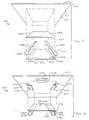
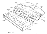
- FIG. 9 is an exploded view of a fourth preferred embodiment thin film warming assembly 700 in accordance with the present invention.
- the assembly 700 comprises a cook top 710 similar to the previously described cook top 410.
- the cook top 710 provides a top cooking, heating, or warming surface 712 and an underside surface 714.
- the assembly 700 further comprises a substrate 740 and a resistive film 720 deposited or otherwise disposed thereon.
- the assembly 700 is particularly well suited for placement upon a mounting channel 750 such as provided by an appliance, the mounting channel having an upper surface 752 and a lower surface 754.
- the mounting channel 750 is typically horizontally disposed along an upper region in most domestic ranges or ovens.
- the substrate 740 and the resistive film 720 are held or secured to the cook top 710 by a bouquet spring assembly 760.
- the spring assembly 760 comprises one or more resilient clamping legs 762 extending radially outward from a center support member 766. Each clamping leg 762 preferably provides a separate clamping member 764 that engages the substrate 740 or connecting members projecting therefrom. Most preferably, each clamping member 764 engages an edge of the substrate 740 and prevents movement thereof.
- the spring assembly 760 comprises four clamping legs 762, extending generally horizontally outward from a center support member 766 and spaced from each other by 90°, and four corresponding clamping members 764.
- the distance between the clamping members 764 of opposite legs 762 is approximately the same as the respective dimension of the substrate 740 to be retained by the spring assembly 760. It is particularly preferred that the clamping members 764 are formed from an electrically insulating material. Examples of suitable dielectric materials include, but are not limited to, steatite, porcelain, or a phenolic-based polymeric material reinforced with glass fibers. As will be understood, there are numerous techniques for affixing the substrate 740, carrying the resistive film 720 thereon, to the spring assembly 760. The clamping members 764 may be attached to the substrate 740 by an adhesive or mechanical fasteners, and then the clamping members 764 affixed to the corresponding distal ends of the clamping legs 762 by adhesive or fasteners. It is also envisioned that the clamping members 764 could be integrally formed with the spring assembly 760.
- FIG. 10 is an elevational view of the fourth preferred embodiment thin film warming assembly 700 when fully assembled.
- FIGS. 9 and 10 do not explicitly illustrate the bus bars, it is to be understood that the assembly 700 comprises one or more bus bars similar to the previously described bus bars 430, 530, and 630 utilized in the assemblies 400, 500, and 600 described herein. Accordingly, the preferred connection configuration shown in FIG. 7A or others described herein may be utilized in conjunction with the bus bars for the assembly 700.
- All of the previously described warmer assemblies 400, 500, 600, and 700 are preferably powered and operated via a temperature controller that regulates the temperature of the warming surface of the assembly between 40°C and 200°C.
- the warmer assembly may comprise a temperature sensor to provide closed loop control.
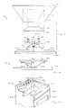
- FIG. 11 illustrates a preferred embodiment range 800 comprising an enclosure 810 having a door 830 pivotally mounted thereon.
- the door 830 provides access to an interior chamber such as an oven (not shown). Such chamber is accessed by opening the door 830 by use of a handle 832.
- the range 800 may also comprise one or more controls 820 and indicators 822 as known in the art.
- the range 800 further comprises one or more heating elements 840 disposed upon or immediately below a cook top 860.
- the range 800 comprises four heating elements 840.
- the heating elements 840 may be in the form of conventional electrical resistance elements known in the art, or in accordance with the present invention thin film heating assemblies described herein, such as the thin film heating assemblies 110, 112, and 118.
- the range 800 also preferably comprises a warming element 850 that provides an upper warming surface 852.
- the warming element preferably corresponds to any one of the previously described warming assemblies 400, 500, 600, or 700. It is most preferred to incorporate the warming element 850 in combination with four heating elements 840 as illustrated in FIG. 11. Although the warming element 850 is shown as centrally disposed between the four heating elements 840, other configurations are included within the scope of the present invention.
- Another particularly preferred heating assembly in accordance with the present invention comprises a planar substrate such as the previously described substrate 120 or cook top such as the previously noted cook top 410, 510, 610, or 710, that comprises glass ceramic of Ceran type in combination with a thin electrically resistive film of tin oxide deposited or otherwise disposed on the glass ceramic.
- This combination and layered configuration is well suited for use as a cooking unit in a griddle, an oven, a heating element, or as a warming element.
- heating and warming assemblies described herein utilize the electrically resistive film disposed on an opposite side of a substrate or cook top from the side upon which cooking occurs
- the present invention includes variations in which the resistive film is disposed on the same side of the substrate or cook top as the cooking surface.
- the present invention also includes a heating or warming assembly having an outermost top layer that is electrically conductive.
- This electrically conductive top layer is preferably connected to an electrical ground. The use of such an electrically conductive outermost top layer connected to a ground, safeguards against accidental electrical shorting or discharge through a metal container on the assembly to an individual.
- thermochromic materials pigments, or inks be incorporated in one or more layers of the previously described assemblies.
- thermochromic materials would be incorporated in a dielectric top layer for a glass ceramic cook top.
- the dielectric layer, containing the thermochromic materials should be confined to the heating zones and preferably, would exhibit a color change to red upon heating.
- a heating assembly in accordance with the present invention comprising a substrate of porcelainized steel and a resistive film of tin oxide was continuously cycled at 260°C for more than 7500 hours, without any significant change in performance. Cycling was performed at 260°C and included energizing the heating assembly for 45 minutes followed by deenergizing the assembly for 15 minutes. It is surprising and remarkable that such cycling could be performed over such a long period of time without degradation of performance. This feat is even more remarkable since the cycling was performed at 260°C.
- the present invention provides electrically powered thin film heating elements that are both reliable and serviceable.
- the elements provide excellent heating characteristics and performance.
- the elements are particularly amenable for incorporation in domestic and industrial heating or cooking appliances.
Abstract
Description
- The present invention relates to electric heating assemblies comprising a thin resistive film. The present invention assembly finds wide application in cooking appliances and related devices.
- Film heating elements comprising a layer of an electrically conductive metal are known such as disclosed in U.S. Patent 2,564,709 to Mochel which is herein incorporated by reference. Such film heating elements have typically been used for defrosting circuits on vehicular window assemblies. Other types of film heating devices are known, such as those disclosed in U.S. Patent 4,536,645 to Mio et al., which is herein incorporated by reference.
- Film heating elements have not found acceptance within the appliance industry although several film devices have been disclosed such as in U.S. Patents 4,889,974 to Auding et al. and 4,298,789 to Eichelberger et al., both of which are herein incorporated by reference. This is believed to result from a lack of reliability and serviceability associated with most contemplated film heating elements. Thus, there is a need for an assembly utilizing a film heating element that is both reliable and serviceable. Furthermore, it would be desirable to provide a film heating assembly that could be readily adapted and utilized in a wide variety of appliance applications.
- The present invention achieves all of the foregoing objectives and provides in one aspect, a heating assembly comprising a planar substrate, a thin electrically resistive film disposed on the substrate, and a non-stick layer disposed on an opposite side of the substrate. The resistive film may comprise a metal oxide or doped metal oxide. The non-stick layer may comprise polytetrafluoroethylene. One or more electrically insulating layers can be disposed between the resistive film and the substrate or on the top side of the substrate. The heating assembly may also comprise electrically conductive electrodes in electrical association with the resistive film, the electrodes preferably comprising a cermet-based silver thick film material. The substrate may comprise porcelainized carbon steel, porcelainized ferritic stainless steel, aluminum oxide, glass ceramic designated under the trade name Ceran, Si3N4-ceramic, or combinations thereof.
- In another aspect, the present invention provides a warming assembly comprising a substrate such as for example an appliance cook top, a thin electrically resistive film in thermal association with the cook top, and at least two electrically conductive electrodes in electrical association with the resistive film. The appliance cook top may comprise a glass ceramic material. One or more layers of an electrically insulating adhesive material may be disposed around the resistive film. Alternatively, various clamping assemblies can be utilized for maintaining the resistive film in thermal association with the cook top. The warming assembly may further comprise an appliance mounting channel by which the warming assembly is supported.
- In yet another aspect, the present invention provides cooking appliances comprising the noted heating and warming assemblies. In one embodiment, an appliance is provided comprising a planar heating or warming assembly that provides a cooking surface, an enclosure for supporting and containing the assembly, and a controller for adjusting and maintaining the temperature of the assembly. In another embodiment, an appliance is provided that comprises a glass ceramic cook top in conjunction with the noted heating or warming assemblies. In another embodiment, an appliance is provided that utilizes one or more of the heating assemblies as heating panels disposed within an oven interior. The present invention also provides appliances utilizing the noted heating or warming assemblies in combination with conventional heating elements known in the art.
-
- FIG. 1 is an exploded view of a first preferred embodiment thin film heating assembly in accordance with the present invention;
- FIG. 1A is a partial perspective view of an alternate preferred embodiment thin film heating assembly;
- FIG. 2 is a cross-sectional view of the first preferred embodiment thin film heating assembly taken along line 2-2 in FIG. 1 after fabrication;
- FIG. 2A is a cross-sectional view of another preferred embodiment thin film heating assembly;
- FIG. 3 is a perspective view of a heating device utilizing a thin film heating assembly in accordance with the present invention;
- FIG. 4 is a perspective view of a range utilizing a plurality of thin film heating assemblies in accordance with the present invention;
- FIG. 4A is a front perspective view of a range illustrating a selectively positionable thin film heating assembly in accordance with the present invention;
- FIG. 5 is an exploded view of the underside of a first preferred embodiment thin film warming assembly in accordance with the present invention;
- FIG. 6 is a cross-sectional view of the first preferred embodiment thin film warming assembly shown in FIG. 5 taken along line 6-6;
- FIG. 7 is an exploded view of a second preferred embodiment thin film warming assembly in accordance with the present invention;
- FIG. 7A is a detailed view of a first preferred end connection at a bus bar utilized in the thin film warming assembly illustrated in FIG 7;
- FIG. 7B is a view illustrating a second preferred embodiment electrical connector assembly in accordance with the present invention;
- FIG. 7C is a partial perspective view of the electrical connector assembly illustrated in FIG. 7B;
- FIG. 7D is a view illustrating a third preferred embodiment electrical connector assembly in accordance with the present invention;
- FIG. 8 is an exploded view of a third preferred embodiment thin film warming assembly in accordance with the present invention;
- FIG. 9 is an exploded view of a fourth preferred embodiment thin film warming assembly in accordance with the present invention;
- FIG. 10 is an elevational view of the fourth preferred embodiment thin film warming assembly shown in FIG. 9; and
- FIG. 11 is a perspective view of a range comprising a thin film warming element in accordance with the present invention.
-
- The present invention provides heating and warming assemblies that utilize a thin electrically resistive film. As referred to herein, the term "thin film" generally refers to films having a thickness from about 0.1 to about 1.0 micrometers. The term "thick film" as used herein, refers to films having a thickness from about 1.0 to about 25 micrometers. In the assemblies described herein, the term "heating assembly" generally refers to an assembly that is capable of providing a temperature of between about 200°C and about 350°C along its heating surface. The heating assemblies described herein may be designed and constructed so that they are operable at temperatures higher than 350°C, such as up to about 400°C. The term "warming assembly" as used herein generally refers to an assembly that is capable of providing a surface temperature between about 40°C and about 200°C along its heating surface.
- The preferred embodiment thin film heating assemblies of the present invention generally comprise (i) a substrate, (ii) a resistive film for heat generation in thermal association with the substrate, (iii) one or more electrically conductive electrodes or bus bars in electrical association with the resistive film, and (iv) a non-stick layer disposed on the exposed surface(s) of the assembly. The preferred embodiment thin film heating assemblies may further comprise (v) one or more dielectric or electrically insulating layers disposed on one or both sides of the resistive film (ii), or on the substrate side that is opposite the substrate side facing the resistive film. In some applications, it may also be preferred to provide an electrically conductive layer on the substrate side opposite the substrate side facing the resistive film. This is described in greater detail below.
- FIG. 1 is an exploded view of a first preferred embodiment thin
film heating assembly 110 in accordance with the present invention. Before describing the particulars of the various preferred embodiments, it is to be noted that the accompanying figures are not necessarily to scale. In many of the figures, the thickness of the resistive film and other layers has been exaggerated to better illustrate the structure and relationship of the various components. In actual practice however, the resistive film may be several orders of magnitude thinner than other components of the assemblies such as for instance the substrate. This aspect is described in greater detail below. Referring to FIG. 1,assembly 110 comprises asubstrate 120, one or moreresistive films 130 disposed on one side of thesubstrate 120 and in thermal association with thesubstrate 120, one or moreouter electrodes 140 that are in electrical association with theresistive films 130 and disposed on the same side of thesubstrate 120 as theresistive films 130, one or moreinner electrodes 150 that are also in electrical association with theresistive films 130 and disposed on the same side of thesubstrate 120 as theresistive films 130 and theouter electrodes 140, and anon-stick layer 160 disposed on a side of thesubstrate 120 opposite the substrate side facing theresistive films 130 and theelectrodes - The
substrate 120 is preferably planar having a first or outer (upper)face 122, an oppositely directed second or inner (lower)face 124, and aperipheral edge 121. Although thesubstrate 120 is depicted in FIG. 1 as rectangular in shape, it is to be understood that thesubstrate 120 may have nearly any shape including circular, oval, and elliptical shapes. The thickness of thesubstrate 120 is generally dictated by the end use requirements for theassembly 110. Typical thicknesses for thesubstrate 120 range from about 0.5 millimeters up to about 1 centimeter. It is preferred that the thickness of thesubstrate 120 is generally uniform. Although it is generally preferred that thesubstrate 120 is flat, it is contemplated that one or both sides of the substrate could be curved or otherwise nonplanar. - Another preferred configuration for the
substrate 120 is generally planar having one finished, relatively smooth face and a second dimpled face. This configuration is typical for substrates of glass ceramic, particularly those available under the designation Ceran. When a substrate having such a configuration is incorporated into the assemblies of the invention and so utilized assubstrate 120 inassembly 110 for instance, the smooth face of the substrate serves as the outer orupper face 122 and the dimpled face serves as the inner orlower face 124. - The
resistive films 130 each have atop surface 132 and abottom surface 134. As noted, multipleresistive films 130 can be utilized in the present invention assemblies. It is preferred that allfilms 130 be disposed in the same plane. It is also preferred that thetop surface 132 of eachresistive film 130 be directed toward, and most preferably immediately adjacent and in contact with, thesecond face 124 of thesubstrate 120. The configuration promotes thermal conduction between theresistive films 130 and thesubstrate 120. It is also preferred that the entirety or at least a majority of the surface area of thesecond face 124 be covered by theresistive films 130. Accordingly, the collective shape resulting from theresistive films 130 is preferably similar to the shape of thesubstrate 120. The preferred thickness for theresistive films 130 is described below. - The
outer electrodes 140 andinner electrodes 150 are preferably straight or linear and oriented parallel with the plane of thesubstrate 120. Theelectrodes electrode outer electrode 140 includes an electrical lead ortermination 142, atop face 144, and abottom face 146. Eachinner electrode 150 includes an electrical lead ortermination 152, atop face 154, and abottom face 156. Although FIG. 1 illustrates theouter electrodes 140 as disposed alongside and adjacent an outer edge of theassembly 110, it is to be understood that one or more, or all of theouter electrodes 140 could be disposed near an intermediate region of theassembly 110. Similarly, other configurations for theinner electrodes 150 and the combination of theinner electrodes 150 and theouter electrodes 140 are contemplated. - Referring to FIG. 1A, the present invention includes a wide array of configurations and arrangements for the
resistive film 130 and theelectrodes electrodes alternate assembly 112 can be disposed immediately adjacent thesubstrate 120, and theresistive film 130 disposed and overlying not only thesubstrate 120 but also theelectrodes preferred embodiment electrodes - As shown in FIG. 1, the
non-stick layer 160 includes an outwardly facingsurface 162 and asecond surface 164. The outwardly facingsurface 162 preferably constitutes the exposed heating surface of theassembly 110. Thesecond surface 164 is preferably disposed immediately adjacent and in contact with thefirst face 122 of thesubstrate 120. - The
assembly 110 is preferably powered by appropriate connection to an electrical power source, such as a three-wire 220 volt supply.Assembly 110 is connected to such a source by connecting theouter electrodes 140 to a respective hot line, e.g. H1 or H2, and if desired, aninner electrode 150 can be connected to ground or neutral, e.g. N. Theassembly 110 can also be appropriately connected to other three-wire systems, or to two-wire systems. - FIG. 2 is a cross-sectional view of the first preferred embodiment thin
film heating assembly 110 taken along line 2-2 shown in FIG. 1. As illustrated in FIG. 2, it is preferred that theresistive films 130 are disposed underneath and immediately adjacent thesubstrate 120. The resistivethin films 130 are electrically connected to theelectrodes thin films 130. - FIG. 2A is a cross-sectional view of another preferred embodiment thin film heating assembly 118 in accordance with the present invention. The thin film heating assembly 118 comprises the previously described
substrate 120,resistive films 130, one or moreouter electrodes 140, one or moreinner electrodes 150, and thenon-stick layer 160. The assembly 118 further comprises a dielectric or electrically insulatinglayer 170 disposed between thesubstrate 120 and the layer of theresistive films 130. Alternatively or in addition, the electrically insulatinglayer 170 can be disposed on thebottom surface 134 of theresistive films 130. The electrically insulatinglayer 170 has a size and shape sufficient for it to cover, or substantially so, the components upon which it is disposed. Typically, the components upon which the electrically insulatinglayer 170 is disposed include thesubstrate 120, theresistive films 130, theouter electrodes 140, and theinner electrode 150. Alternatively or in addition, the electrically insulatinglayer 170 may be disposed on the substrate side opposite the substrate side facing the resistive film, i.e.side 122. The thickness of the electrically insulatinglayer 170 primarily depends upon the electrical insulation properties, i.e. the volume resistivity and dielectric constant, of the material forming thelayer 170, and the electrical operating characteristics of the thin film heating assembly 118. The thickness of thelayer 170 may also vary depending upon the particular application, but should in all cases, be sufficiently thick to prevent electrical current loss or short circuiting of theresistive films 130, theouter electrodes 140, and theinner electrodes 150. As described in greater detail below, it may in some applications be preferred to provide an electrically conductive layer on the outermost top surface of the assembly. This layer may be in addition to, or replace, thelayer 170 whenlayer 170 is disposed on the substrate side opposite the substrate side facing the resistive film. - The preferred materials for the various components of preferred heating assemblies in accordance with the present invention are as follows. The substrate (i) can be nearly any heat resistant, relatively rigid material. The material selected for the substrate (i) should also exhibit electrical insulating properties or be coated or otherwise treated to have such property. The material selected for the substrate (i) should have a relatively low coefficient of thermal expansion. Examples of materials suitable for use as the substrate (i) include, but are not limited to, porcelainized carbon steel, porcelainized ferritic stainless steel, aluminum oxide, glass ceramic commonly referred to as Ceran, Si3N4-ceramic, and combinations of the foregoing. A particularly preferred material for the substrate is glass ceramic. A preferred glass ceramic is Li2Al2Si2O6 beta-quartz (LAS), such as available from Eurokera or Schott. If a porcelainized steel is selected for use as the substrate (i), it should be free of alkali and alkali earth metals so as to maintain good electrical insulating properties at temperatures above 150° C. A supplier of such porcelainized steel substrates is Ferro. Glass ceramic is generally preferred since as compared to other substrates, glass ceramic exhibits a relatively low thermal shear stress. The coefficient of thermal expansion of glass ceramic is essentially zero as compared to steel having a coefficient of thermal expansion of about 11 ppm. The use of near zero thermal expansion glass ceramic significantly reduces the tendency of crazing and cracking of other layers or films deposited on the glass substrate such as tin dioxide.
- The electrically resistive film (ii) can be a thin film of metal oxide such as for instance tin dioxide, a cermet-based thick film material, a polymer-based thick film material, or any type of electrically resistive film or coating. It is preferred that the resistive film (ii) is a thin film of metal oxide, and most preferred that the metal oxide thin film be a doped tin dioxide thin film. A preferred dopant for tin dioxide is 0.1 to 0.5 weight percent fluorine. It is also preferred that the metal oxide thin film be deposited on a face of the substrate (i) by an atmospheric chemical vapor deposition (ACVD) process. One preferred metal oxide for example, is tin dioxide thin film doped with approximately 0.4 weight percent fluorine, and applied by an atmospheric chemical vapor deposition process at approximately 550°C. It is contemplated that other techniques for depositing the resistive film (ii) could be utilized. For instance, liquid materials or resistive film precursors could be applied by spraying and if necessary followed by additional spray coatings, exposure to heat or radiation, or other operations depending upon the end use application.
- The material utilized for forming the resistive film (ii) has a positive temperature coefficient (PTC) with respect to its electrical resistance. When utilizing a metal oxide such as tin oxide, the temperature coefficient of resistance may be adjusted by adding appropriate amounts of oxides of iron, cobalt, nickel, niobium, tantalum, zirconium, and hafnium. It is important that the resistive film (ii) exhibit a PTC so that electrical resistance of the film increases with temperature. This property prevents temperature runaway during application of electrical power to the heating assembly. It is preferable to utilize a resistive film that has a linear PTC in the range of 25° to 400°C. Doped tin dioxide exhibits this property. The resistive film (ii) should be able to accommodate a power density of between about 1.0 to about 20 W/cm2 and a current density of between about 11,000 to 90,000 A/cm2.
- The thickness of the resistive film (ii) varies depending upon the materials utilized for the resistive film (ii) and the particular application. The preferred thickness of such films generally ranges from about 0.1 to about 0.5 micrometers for most metal oxides or doped metal oxides, including tin dioxide. The thickness of the resistive film when formed from a thick-film material, for instance a cermet-based thick film material or a polymer-based thick film material, is between about 1 and about 25 micrometers.
- A tin dioxide thin film may be applied to the dimpled underside of a Ceran type glass ceramic substrate. Although not wishing to be bound to any particular theory, it is believed that superior adhesion is achieved between a thin film and a dimpled or irregular surface substrate as compared to a substrate having a smooth surface. A dimpled surface has a greater amount of surface area available for bonding than a relatively smooth surface. The increased surface area decreases the wattage or power density carried by the thin film and so, promotes reliability of the thin film. The dimpled surface also prevents or minimizes fractures of the substrate. By depositing a thin film directly on the dimpled face of a substrate, the occurrence of scratches or fissures in the thin film is reduced. Since there is essentially no tensile stress at the peaks or high points of the dimples, the propagation of cracks in the substrate and adjacent films, is significantly minimized. Depositing a thin film directly upon a dimpled surface is preferred as compared to applying a thick film cermet material or adhesive material on the dimpled surface, since deposition of a thin film does not produce differential stresses on the glass ceramic and resulting shear and fracture. Furthermore, the dimpled surface promotes gripping for an electrical edge connector used for transmission of electrical power to the thin film layer. Moreover, direct deposition of a thin film on a dimpled substrate surface avoids having to smooth or otherwise finish the dimpled surface. This will in many applications provide significant economic advantage. It may in some instances be desirable to apply an intermediate dielectric layer between the underside of the Ceran substrate and the tin dioxide film.
- It is preferred that a dimpled substrate have a particular configuration as follows. For a substrate having a thickness from about 4 to about 5 millimeters, the dimpled surface preferably comprises a plurality of closely arranged dimples that project outward a distance of from about 40 to about 200 micrometers from the substrate surface. Each dimple is preferably oval shaped and oriented so that its major diameter is parallel with the longitudinal axis of the substrate. It is most preferred that all of the dimples, or at least a majority, be oriented parallel to one another and with the longitudinal axis of the substrate. The preferred major diameter for each oval is about 2.1 millimeters. The preferred minor diameter of each oval is about 1.75 millimeters. The ovals are preferably spaced from each other by about 3.4 millimeters between centerpoints of adjacent dimples as measured along their width or minor diameter, and about 2.5 millimeters between centerpoints of adjacent dimples as measured along their length or major diameter.
- The electrodes or bus bars (iii) are preferably formed from a cermet-based silver thick film material. It is contemplated that other electrically conductive materials could be utilized for the electrodes (iii). The selected materials should be compatible with other materials utilized in the resulting heating assembly. A preferred material for the electrodes is a silver cermet. This preferred material is applied by screen printing. In its printable state, it comprises a carrier or solvent, glass frit, and silver particles. When deposited on a glass substrate and fired at approximately 550°C, it forms a blend with the glass substrate as a continuous phase with the silver particles dispersed therein. Silver cermet materials are available from DuPont, ESL, and Ferro for example.
- The non-stick layer (iv) is preferably formed from crosslinked silicone or polytetrafluoroethylene (PTFE) impregnating a porous scratch resistant structure like flame sprayed stainless steel. Various crosslinked silicone compositions may be utilized for the non-stick layer (iv).
- The optional dielectric layer (v) is preferably any electrically insulating material that is suitable for exposure to relatively high temperatures, such as generated by the heating assemblies described herein. Examples of such materials include silicone dioxide, titanium dioxide, inorganic high temperature cements, sealing glasses, sol gel applied ceramics such as zirconia applied as a sol gel, high temperature paint, plasma or flame sprayed ceramics, or combinations thereof. The dielectric material selected preferably has a coefficient of thermal expansion as close to the substrate (i) as possible. A specific example of a preferred material for the dielectric layer is a glass layer fused to a glass ceramic substrate. Such fusing can be performed at temperatures in the range of 600°C to 850°C. Another specific example of a preferred material for the dielectric layer is a thin film of titanium dioxide TiO2. This can be applied via atmospheric chemical vapor deposition. A further specific example of a preferred material for the dielectric layer is a ceramic material, for instance an alumina-based ceramic material, that is plasma sprayed or HVOF sprayed. Another specific example of a preferred material is zirconium dioxide (ZrO2) that is applied as a sol gel.
- The optional dielectric layer (v) can be incorporated into any of the heating or warming assemblies described herein. Multiple dielectric layers may be utilized where necessary. A preferred location for incorporating one or more electrically insulating layers in the assemblies described herein is between the electrically resistive film (ii) and the substrate (i) and on the upper substrate side.
- As noted, the present invention includes assemblies comprising a top or outermost layer of an electrically conductive material. It may in some applications, be desirable to provide an electrical connection between that top electrically conductive material and an electrical ground. A preferred material for this top electrically conductive grounding layer is ACVD fluorine doped tin dioxide (SnO2) thin film having a thickness of from about 0.1 to about 0.5 micrometers, or an Invar-alloy film, for example Fe-Ni, having a thickness of from about 0.1 to about 10 micrometers.
- Any or all of the electrode or bus bars (iii), the non-stick layer (iv), and/or the dielectric layer (v), and the optional safety ground layer can be formed by screen printing techniques, spray coating operations, or other suitable techniques depending upon the characteristics of the starting materials. For applications in which the electrodes or bus bars (iii) are formed from an initially flowable material, such as thick film paste materials, it is preferred to screen print the electrode material directly onto the surface of interest. This enables formation of any desired arrangement or pattern of electrodes or bus bars in a simple and economical fashion.
- The coefficient of thermal expansion (CTE) of components (i) - (iv) and optional dielectric layer (v) and safety ground layer is preferably closely matched. Careful selection of the materials utilized for components (i) - (iv) and the noted optional layers, and appropriate matching of their respective thermal expansion characteristics ensure that the resulting assembly will exhibit high durability and minimal failure occurrences.
- A preferred combination of materials for the various components is as follows. The substrate (i) preferably comprises a glass ceramic. The resistive film (ii) is preferably formed from doped ACVD tin dioxide. A cermet-based silver thick film is utilized for the electrodes or bus bars (iii). The non-stick layer (iv) consists of crosslinked silicone or PTFE impregnating a porous scratch resistant structure like flame sprayed stainless steel or plasma sprayed ceramic.
- Heating by the thin film heating assemblies, such as
assembly 110, is performed by passing electrical current through theresistive film 130. This is preferably achieved by electrically connecting theelectrical leads 142 to a voltage source. A controller can be used to regulate the flow of electric current to control the temperature of the resistive film or the heating assembly. If utilizing doped tin oxide for the resistive film (ii), the linear PTC characteristic of that material enables direct temperature control by monitoring the change in current versus temperature change. - The present invention also provides appliances that employ the previously described thin film heating assemblies. FIG. 3 illustrates a
griddle 200 comprising a thinfilm heating assembly 210, one ormore controls 220, and anenclosure 230. The thinfilm heating assembly 210 is preferably similar to the previously described heating assemblies. Theheating assembly 210 is incorporated within theenclosure 230 by techniques known to those skilled in the art. - FIG. 4 illustrates a
domestic range 300 comprising a plurality of thin film heating assemblies in accordance with the present invention. Therange 300 comprises a planar, relatively largesurface area griddle 310 utilizing a thin film heating assembly such as the previously describedheating assembly 210. Moreover, therange 300 may comprise one or moreoven heating panels 330 disposed in the lower portion of therange 300 that employ the thin film heating assembly of the present invention. Theseoven heating panels 330 are described in greater detail below. Therange 300 may utilize any combination of thegriddle 310 and theoven heating panels 330. Therange 300 may further comprise one or moreheating element elements 348 in the form of conventional electrical resistance elements known in the art, or in accordance with the present invention thin film heating assemblies. Therange 300 generally comprises anenclosure 340, adoor 346 pivotally attached thereto, and indicators andelectronic controls griddle 310, theoven heating panels 330, and theheating element elements 348. - The thin film heating assembly of the present invention is particularly well suited for use as an oven heating panel that can supplement and most preferably replace conventional oven baking elements. Replacing conventional oven baking elements with the heating assembly of the present invention provides an oven that is significantly easier to clean. The non-stick outer surface of a thin film heating assembly that is incorporated into an oven heating panel and elimination of conventional baking elements facilitate cleaning the oven after use. Replacement of conventional baking elements with a heating panel utilizing the thin film heating assembly increases the effective oven volume. Moreover, replacement of conventional baking elements with a heating panel utilizing the thin film heating assembly results in energy savings and promotes temperature uniformity within the oven interior.
- Referring to FIG. 4, the
oven heating panels 330 can be disposed along any wall or portion thereof within the oven interior. Preferably, one or more oven heating panels are disposed along the rear wall of the oven interior. Similarly, one or more oven heating panels are located on the bottom wall of the oven interior, preferably replacing a conventional lower baking element. Likewise, one or more oven heating panels are located on the top wall of the oven interior, preferably replacing a conventional upper heating element such as a broiling element. It is also contemplated to incorporate one or more heating panels on the inward facing surface of theoven door 346. All of the noted oven heating panels could be employed in any combination. Thus, the present invention includes a range or oven comprising a plurality ofoven heating panels 330 disposed on any combination of surfaces defining the oven interior. It is also contemplated that a plurality ofoven heating panels 330 may be located on a single wall or common surface of the oven interior. This may be desirable so that exposed noncovered portions of the underlying wall such as between spaced apart adjacentoven heating panels 330, can provide mounting or support provisions for oven racks, rotisserie components, lights, viewing windows, or other items. The shape of the oven heating panels is not critical. - It is also preferred that the oven heating panels be provided as movable panels that can be oriented or positioned within the oven interior in any desired configuration. Thus, in an alternate preferred embodiment, a range comprises a plurality of oven heating panels disposed in the lower portion of the oven interior. At least one of the oven heating panels is adapted to be selectively positioned to different locations within the oven interior, much like an oven rack may be placed at various locations within the oven interior. FIG. 4A illustrates an alternate
preferred embodiment range 305 comprising one or more selectively positionableoven heating panels 332. Therange 305 preferably comprises many of the same components as previously described with respect to therange 300 shown in FIG. 4, such as thegriddle 310, one or moreoven heating panels 330, one or moreheating element elements 348, anenclosure 340, adoor 346, one ormore indicators 342, and one ormore controls 344. Therange 305 further comprises a selectively positionableoven heating panel 332 that can be placed at various locations within the oven interior. Therange 305 will typically include one or moreupper racks 320 disposed near the upper portion of the oven interior, and one or morelower racks 322 disposed near the lower portion of the oven interior. As evident in FIG. 4A, it is preferred that the interior side walls of the oven provide horizontally extending support ridges orledges 324 for supporting an upper orlower oven rack oven heating panel 332. - The selectively positionable
oven heating panels 332 can be placed at any location within the interior of the oven provided sufficient supports are provided at the desired location such as a pair ofsupport ridges 324. This feature of a selectively positionable heating panel provides significantly greater flexibility in heating or baking operations than with conventional ovens utilizing non-positionable heating elements. - Referring further to FIG. 4A, the positionable
oven heating panel 332 may be moved to a new location within the oven interior, such aslocation 334 depicted in FIG. 4A by dashed lines, by sliding or otherwise removing thepanel 332 outward from the oven interior, as one would remove an oven rack such asupper rack 320, and then placing thepanel 332 at the new location, e.g.location 334, within the oven interior. - Electrical connections are established to the selectively positionable
oven heating panel 332 by known techniques. For instance, a flexible cable housed within an appropriate flexible cover or conduit, can be used to provide both electrical power and control signals to thepanel 332. The flexible cable may extend from a rear wall of the oven interior to a rearwardly directed edge or the underside of thepanel 332. Alternately, a plurality of plug receptacles could be provided on one or more walls of the oven interior, and one or more corresponding mating receptacles provided on thepanel 332 such that upon appropriate placement of the panel, such as between a pair ofsupport ridges 324 and against the oven rear wall, the plugs are engaged thereby completing the requisite power and control circuits between thepanel 332 and therange 305. - The
oven heating panel oven heating panel - The present invention also provides a warming assembly comprising a thin electrically resistive film. The warming assembly is particularly well suited for providing a warming zone on a cook top and preferably a smooth planar cook top such as used in modern ranges and cooking appliances. FIG. 5 is a perspective view of the underside of a first preferred embodiment thin
film warming assembly 400 in accordance with the present invention. Theassembly 400 comprises acook top 410, a thin electricallyresistive film 420 disposed on the underside of thecook top 410, and one ormore bus bars 430 in electrical association with theresistive film 420. Thecook top 410 has a top heating surface 412 upon which is typically placed containers or food items to be heated or warmed, and a cooktop underside 414. Thecook top 410 is preferably a glass ceramic cook top as known in the art. Theresistive film 420 corresponds to thethin film 130 of the previously described thin film heating assemblies. Theresistive film 420 is preferably tin dioxide. Theresistive film 420 has anupper surface 422 and alower surface 424. Theresistive film 420 is preferably deposited on the underside of thecook top 410 such that theupper surface 422 of theresistive film 420 is in contact with the cooktop underside 414. The bus bars 430 correspond to the previously describedelectrodes bus bar 430 comprises atermination pad 432 at which external electrical connections to thebus bar 430 are established. - FIG. 6 illustrates a cross-sectional view of the first preferred embodiment thin
film warming assembly 400 shown in FIG. 5 taken along line 6-6. Again, it will be appreciated that the illustration is not necessarily to scale. It is to be understood that although FIGS. 5 and 6 depict theresistive film 420 in a stacked or overlying relationship with the bus bars 430, alternate configurations are included in the present invention. - The present invention warming assembly also includes embodiments in which the electrically resistive heating film is secured to or deposited upon a substrate, and the resulting assembly then joined or otherwise brought into heat transfer relationship with a cook top. FIG. 7 is an exploded view of a second preferred embodiment of a thin
film warming assembly 500 having such a configuration. Theassembly 500 comprises acook top 510 similar to the previously describedcook top 410. Thecook top 510 provides a top cooking, heating, or warmingsurface 512 and anunderside surface 514. Theassembly 500 further comprises asubstrate 540 and aresistive film 520 deposited or otherwise disposed thereon. Thesubstrate 540 corresponds to the previously describedsubstrate 120, and provides afirst face 542 and asecond face 544. Theresistive film 520 corresponds to the previously describedresistive film 130, and includes anupper surface 522 and alower surface 524. Theassembly 500 further comprises anadhesive layer 550 disposed between thecook top 510 and theresistive film 520 for securing and maintaining those components in heat transfer relationship with each other. Theadhesive layer 550 includes atop surface 552 and abottom surface 554. Most preferably, theadhesive layer 550 is disposed between theunderside 514 of thecook top 510 and theupper surface 522 of theresistive film 520. Theadhesive layer 550 can be formed from nearly any adhesive suitable for the end use conditions for theassembly 500. Preferably, the adhesive used for theadhesive layer 550 is a heat conductive, heat resistant, two component silicone elastomer. It is also contemplated that appropriate heat resistant one component silicone elastomer compositions may be used. Most preferably, theadhesive layer 550 is electrically insulating. Theassembly 500 also comprises one ormore bus bars 530 in electrical association with theresistive film 520. The bus bars 530 each provide atermination area 532 and correspond to the previously describedelectrodes resistive film 520 as shown in FIG. 7. Other affixment techniques besides the use of adhesives could be employed for securing theresistive film 520 to thecook top 510. It will be appreciated that although FIG. 7 illustrates theresistive film 520 in a stacked or overlying relationsh-ip with the bus bars 530, alternate configurations are included in the present invention. - FIG. 7A is a detailed exploded view of a preferred end connection at a
bus bar 530 of theassembly 500 shown in FIG. 7. In this preferred end connection configuration, thebus bar 530 comprises aninclined segment 534 extending between thebus bar termination 532 and the major portion of thebus bar 530. Theinclined segment 534 is angled away from theunderside 514 of thecook top 510 so as to provide a clearance space between thebus bar 530 and theunderside 514 of thecook top 510. One or moreelectrical leads 570, each providing aring terminal 572 at their end, are connected to thebus bar 530 and specifically to thebus bar termination 532 by a threadedfastener 574 andnut 576. Upon insertion of thefastener 574 through the opening in thering terminal 572 and anaperture 536 defined in thetermination 532, and placement and engagement of thenut 576 with thefastener 574, an electricallyinsulating end cap 578 is preferably disposed over the end of thefastener 574. Theend cap 578 can be formed from nearly any electrically insulating flexible material. A heat resistant silicone rubber tubing has been found useful for theend cap 578. - Instead of utilizing a threaded fastener and nut assembly as shown in FIG. 7A, it is also within the scope of the invention to utilize a rivet connection between an electrical lead, such as
lead 570 in FIG. 7A, and thebus bar termination 532. It is also contemplated that the bus bar or electrode could be disposed immediately adjacent to the substrate or cook top instead of being spaced therefrom as shown in FIG. 7A. An aperture is then preferably provided at the location for attachment of an electrical lead, and a fastener or rivet inserted therethrough. An electrically insulating washer or fastener can be used at the point of attachment between the electrical lead and bus bar, so that the portion of the fastener or rivet on the opposite side of the substrate is electrically isolated from the electrical lead and bus bar. - The present invention includes additional coupling assemblies for providing electrical connection between the thin film heating or warming assembly and the appliance, or at least the power supply leads. A second preferred embodiment
electrical coupling assembly 1000 is illustrated in FIGS. 7B and 7C. The second preferred embodimentelectrical coupling assembly 1000 comprises areceptacle 1010 affixed to a heating or warming assembly as described herein. FIGS. 7B and 7C illustrate theelectrical coupling assembly 1000 affixed to asubstrate 1040, and in electrical association with aresistive film 1050. Thereceptacle 1010 may be a conventional female plug coupler as known in the art and available from Amp. Thereceptacle 1010 provides a receivingchamber 1012 for releasably engaging a corresponding male connector. Thereceptacle 1010 comprises one or moreelectrical conductors 1030 accessible from the receivingchamber 1012. Theconductors 1030 extend to, or are in electrical association with, a corresponding number ofbus bars 1032, such as disposed on the underside of theresistive film 1050. Theelectrical conductors 1030 are preferably electrically connected to therespective bus bars 1032 at a corresponding number oftermination regions 1034. All electrical connections between theconductors 1030 and the busbar termination regions 1034 are preferably achieved by soldering. Theconnector assembly 1000 is utilized to selectively establish electrical connections between the heating or warming assembly and the appliance or product enclosure. The electrical connections may be for power supply connections or for control signal or electrical measurement connections. - FIG. 7B also illustrates a mounting configuration for a heating or warming assembly of the present invention. One or
more enclosure panels 1060 such as constituting an appliance enclosure may be formed to provide a generallyhorizontal lip 1062 upon which the heating or warming assembly is mounted and affixed. Employing this mounting approach, the previously described receptacle 1010 can be affixed to theenclosure panel 1060. Other techniques for mounting a heating or warming assembly within an enclosure can be utilized including for instance threaded fasteners and rivets. - A third preferred embodiment electrical coupling assembly 1100 is illustrated in FIG. 7D. This third preferred embodiment coupling assembly 1100 comprises a dual
prong union member 1110 having a first projection 1112 and asecond projection 1114, both projections for establishing electrical connection therebetween. Theunion member 1110 further has a resilient mountingmember 1120 adapted for affixment to anenclosure panel 1130 or anenclosure mounting frame 1132. As shown in FIG. 7D, theunion member 1110 is attached to a heating or warming assembly described herein, preferably by welding or brazing the mountingmember 1120 to a peripheral edge or lip of theenclosure panel 1130 or to a region of theenclosure mounting frame 1132. The mountingmember 1120 may be affixed to a heating or warming assembly by mechanical fasteners such asrivets 1134 shown in FIG. 7D. Once attached, thesecond projection 1114 should contact a termination region of a bus bar or other electrical component. Accordingly, electrical connection to the bus bar at thesecond projection 1114 is made at the first projection 1112. It is to be understood that the coupling assemblies described herein are exemplary, and the present invention heating and warming assemblies may utilize nearly any type of electrical connector to establish power, signal, or other electrical current flows to and from the heating or warming assembly. - FIG. 8 is an exploded view of a third preferred embodiment thin
film warming assembly 600 in accordance with the present invention. Theassembly 600 comprises a cook top 610 similar to the previously describedcook top 410. The cook top 610 provides a top cooking, heating, or warmingsurface 612 and anunderside surface 614. Theassembly 600 further comprises asubstrate 640 and aresistive film 620 deposited or disposed thereon. Thesubstrate 640 is similar to the previously describedsubstrate 120, and provides afirst face 642 and asecond face 644. Theresistive film 620 corresponds to the previously describedresistive film 130, and includes anupper surface 622 and alower surface 624. Theassembly 600 further comprises bus bars 630 which correspond to the previously describedelectrodes film 620 opposite the cook top 610. The bus bars 630 are preferably disposed proximate to the opposite edges of theresistive film 620. The termination ends 632 of the bus bars 630 may also be configured as the configuration depicted in FIG. 7A. Alternatively or in addition, electrical connections can be established by the assemblies shown in FIGS. 7B-7D. Thesubstrate 640 andresistive film 620 are affixed to and placed in thermal association with the cook top 610 by one ormore clamps 660. Theclamps 660 enable the assembly ofsubstrate 640, theresistive film 620, and the bus bars 630 to be releasably engaged with the cook top 610. It is preferred to dispose at least one clamp on each peripheral edge of thesubstrate 640 having thefilm 620 disposed thereon. Eachclamp 660 is preferably affixed to theunderside 614 of the cook top 610 by an effective amount of an adhesive 670. The adhesive 670 is preferably a single component heat resistant silicone elastomer known to those skilled in the art. The thinfilm warming assembly 600 includes variant embodiments in which one ormore clamps 660 are affixed to the cook top 610 by mechanical fasteners or other techniques besides the use of adhesives. - FIG. 9 is an exploded view of a fourth preferred embodiment thin
film warming assembly 700 in accordance with the present invention. Theassembly 700 comprises acook top 710 similar to the previously describedcook top 410. Thecook top 710 provides a top cooking, heating, or warmingsurface 712 and anunderside surface 714. Theassembly 700 further comprises asubstrate 740 and aresistive film 720 deposited or otherwise disposed thereon. Theassembly 700 is particularly well suited for placement upon a mountingchannel 750 such as provided by an appliance, the mounting channel having anupper surface 752 and a lower surface 754. The mountingchannel 750 is typically horizontally disposed along an upper region in most domestic ranges or ovens. Thesubstrate 740 and theresistive film 720 are held or secured to thecook top 710 by abouquet spring assembly 760. Thespring assembly 760 comprises one or more resilient clampinglegs 762 extending radially outward from acenter support member 766. Each clampingleg 762 preferably provides aseparate clamping member 764 that engages thesubstrate 740 or connecting members projecting therefrom. Most preferably, each clampingmember 764 engages an edge of thesubstrate 740 and prevents movement thereof. In the most preferred embodiment, thespring assembly 760 comprises four clampinglegs 762, extending generally horizontally outward from acenter support member 766 and spaced from each other by 90°, and fourcorresponding clamping members 764. The distance between the clampingmembers 764 ofopposite legs 762 is approximately the same as the respective dimension of thesubstrate 740 to be retained by thespring assembly 760. It is particularly preferred that the clampingmembers 764 are formed from an electrically insulating material. Examples of suitable dielectric materials include, but are not limited to, steatite, porcelain, or a phenolic-based polymeric material reinforced with glass fibers. As will be understood, there are numerous techniques for affixing thesubstrate 740, carrying theresistive film 720 thereon, to thespring assembly 760. The clampingmembers 764 may be attached to thesubstrate 740 by an adhesive or mechanical fasteners, and then the clampingmembers 764 affixed to the corresponding distal ends of the clampinglegs 762 by adhesive or fasteners. It is also envisioned that the clampingmembers 764 could be integrally formed with thespring assembly 760. - FIG. 10 is an elevational view of the fourth preferred embodiment thin
film warming assembly 700 when fully assembled. Although FIGS. 9 and 10 do not explicitly illustrate the bus bars, it is to be understood that theassembly 700 comprises one or more bus bars similar to the previously describedbus bars assemblies assembly 700. - All of the previously described
warmer assemblies - Other electrical design consideration and aspects, applicable to many if not all of the assemblies described herein, are disclosed in U.S. application Serial No. __________, filed________________, entitled "SOLID STATE SWITCHING CONTROL FOR LEAKAGE CURRENT CANCELLATION"; and U.S. Patent 5,577,158 both owned by the same assignee of the present invention and herein incorporated by reference.
- The present invention also provides appliances utilizing the previously described warming elements. FIG. 11 illustrates a
preferred embodiment range 800 comprising anenclosure 810 having adoor 830 pivotally mounted thereon. Thedoor 830 provides access to an interior chamber such as an oven (not shown). Such chamber is accessed by opening thedoor 830 by use of ahandle 832. Therange 800 may also comprise one or more controls 820 andindicators 822 as known in the art. Therange 800 further comprises one ormore heating elements 840 disposed upon or immediately below acook top 860. Typically, therange 800 comprises fourheating elements 840. Theheating elements 840 may be in the form of conventional electrical resistance elements known in the art, or in accordance with the present invention thin film heating assemblies described herein, such as the thinfilm heating assemblies range 800 also preferably comprises a warming element 850 that provides anupper warming surface 852. The warming element preferably corresponds to any one of the previously described warmingassemblies heating elements 840 as illustrated in FIG. 11. Although the warming element 850 is shown as centrally disposed between the fourheating elements 840, other configurations are included within the scope of the present invention. - Another particularly preferred heating assembly in accordance with the present invention comprises a planar substrate such as the previously described
substrate 120 or cook top such as the previously notedcook top - Although all the heating and warming assemblies described herein utilize the electrically resistive film disposed on an opposite side of a substrate or cook top from the side upon which cooking occurs, the present invention includes variations in which the resistive film is disposed on the same side of the substrate or cook top as the cooking surface.
- The present invention also includes a heating or warming assembly having an outermost top layer that is electrically conductive. This electrically conductive top layer is preferably connected to an electrical ground. The use of such an electrically conductive outermost top layer connected to a ground, safeguards against accidental electrical shorting or discharge through a metal container on the assembly to an individual.
- It is contemplated that one or more thermochromic materials, pigments, or inks be incorporated in one or more layers of the previously described assemblies. Preferably, such thermochromic materials would be incorporated in a dielectric top layer for a glass ceramic cook top. The dielectric layer, containing the thermochromic materials, should be confined to the heating zones and preferably, would exhibit a color change to red upon heating.
- A series of experiments were conducted in which the response characteristics of heating assemblies in accordance with the present invention were analyzed. In a first trial, a warmer element corresponding to the previously described
warming assembly 400 was connected to an electrical power supply and the temperature measured as the assembly reached its steady state operating temperature. Table 1 set forth below indicates the relationship between the power applied and the resulting temperature as a function of time.Power [W] Steady State [°C] Time to Steady State [Minutes] Time to 120°C [Minutes] Watt Density [W/cm2] 50 107 9.6 0.25 100 167 8.9 4.4 0.51 150 204 8.1 2.5 0.76 200 228 8.1 2.1 1.02 250 264 8.2 1.6 1.27 300 304 8.0 1.2 1.53 - It can be seen from Table 1 that in order to reach a temperature of 120°C, a typical recommended warmer temperature, within a reasonable time, i.e. about 2.0 minutes, a power density of at least 1.0 W/cm2 should be used.
- In a second trial, the response characteristics of a warmer according to the previously described
warming assembly 700 were similarly tested. The results of that testing are set forth below in Table 2 as follows:
- It is evident from the results presented in Table 2 that in order to reach a temperature of 120°C in less than about 7 minutes, a power density of at least 1.18 W/cm2 should be used. It is surprising and remarkable that such low amounts of power can be utilized to rapidly reach the noted temperature. Table 2 also illustrates that even at significantly lower power levels, e.g. 250W and 200W, the warming assembly reached 120°C within relatively short time periods, e.g. 9.5 and 12.5 minutes, respectively.
- In yet another trial, a heating assembly in accordance with the present invention comprising a substrate of porcelainized steel and a resistive film of tin oxide was continuously cycled at 260°C for more than 7500 hours, without any significant change in performance. Cycling was performed at 260°C and included energizing the heating assembly for 45 minutes followed by deenergizing the assembly for 15 minutes. It is surprising and remarkable that such cycling could be performed over such a long period of time without degradation of performance. This feat is even more remarkable since the cycling was performed at 260°C.
- The present invention provides electrically powered thin film heating elements that are both reliable and serviceable. The elements provide excellent heating characteristics and performance. The elements are particularly amenable for incorporation in domestic and industrial heating or cooking appliances.
- While the foregoing details are what is felt to be the preferred embodiments of the present invention, no material limitations to the scope of the claimed invention are intended. Further, features and design alternatives that would be obvious to one of ordinary skill in the art are considered to be incorporated herein. The scope of the invention is set forth and particularly described in the claims herein below.
Claims (39)
- A heating and/or warming assembly for use in a cooking appliance, said assembly comprising:a, preferably planar, substrate having a first face and a second face;a thin electrically resistive film disposed on said first face of said substrate; anda non-stick layer disposed on said second face of said substrate.
- The assembly of claim 1 wherein said substrate comprises one or more materials selected from the group consisting of glass ceramic, porcelainized steel, aluminium-oxide and Si3N4-ceramic.
- The assembly of claim 2 wherein said substrate comprises a first face that is relatively smooth and a second face that is dimpled or wherein said substrate comprises a first face that is dimpled and a second face that is relatively smooth.
- The assembly according to at least one of the preceding claims wherein said electrically resistive film comprises a metal oxide, preferably doped tin dioxide having a preferred thickness of from about 0,1 to about 0,5 micrometers.
- The assembly according to at least one of the preceding claims wherein said non-stick layer comprises polytetrafluoroethylene and/or crosslinked silicone.
- The assembly according to at least one of the preceding claims further comprising:a dielectric layer disposed between said electrically resistive film and said substrate.
- The assembly of claim 6 further comprising:a second dielectric layer disposed on a face of said electrically resistive film opposite said substrate and/or on a top side of said substrate.
- The assembly according to at least one of the preceding claims further comprising:at least two electrically conductive electrodes in electrical association with said electrically resistive film.
- The assembly of claim 8 wherein said electrically resistive film is disposed between said at least two electrically conductive electrodes or wherein said electrically conductive electrodes are disposed between said substrate and said electrically resistive film, said electrically conductive electrodes preferably comprising a cermet-based silver thick film material.
- The assembly of claim 8 or 9 wherein said at least two electrically conductive electrodes are disposed on said resistive film.
- The assembly according to at least one of the preceding claims wherein upon application of electrical current to said electrically resistive film, said non-stick layer reaches a temperature in the range from about 200°C to about 400°C preferably in the range from about 200°C to about 350°C.
- The assembly according to at least one of the preceding claims further comprising:a dielectric layer disposed between said non-stick layer and said substrate.
- A heating and/or warming assembly for use in a cooking appliance, said assembly comprising:a substrate having an upwardly directed first face and an oppositely directed second face;a first dielectric layer disposed immediately adjacent said second face of said substrate;a thin electrically resistive film disposed immediately adjacent said first dielectric layer and preferably comprising doped tin dioxide; anda second dielectric layer disposed immediately adjacent a side of said electrically resistive film opposite said first dielectric layer.
- An assembly for use in a cooking appliance, said assembly comprising:a substrate having an upwardly directed first face and an oppositely directed second face;a layer disposed immediately adjacent said first face of said substrate; anda thin electrically resistive film disposed immediately adjacent said second face of said substrate.
- The assembly of claim 14 wherein said layer is a dielectric layer or an electrically conductive layer, preferably connected to an electrical ground.
- The assembly according to at least one of the preceding claims wherein said second face of said substrate is dimpled.
- A cooking appliance comprising the heating and/or warming assembly according to at least one of the preceding claims.
- The cooking appliance of claim 17 comprising:an electrically powered planar heating and/or warming assembly providing a cooking surface;an enclosure having provisions for supporting said assembly; anda controller for adjusting and maintaining the temperature of said cooking surface by governing the amount of electrical power transferred to said assembly;wherein said assembly includes a planar substrate having a first face and a second face, a thin electrically resistive film disposed on and covering at least a majority of said first face of said substrate and in electrical association with said controller, and a non-stick layer disposed on said second face of said substrate.
- The cooking appliance of claim 17 or 18 further comprising:a second electrically powered heating assembly, said second heating assembly including a planar substrate having a first face, the first face preferable is dimpled, and a second face, and a thin electrically resistive film disposed on said first face of said substrate.
- The cooking appliance according to at least one of the claims 17 to 19 wherein said enclosure further has a plurality of oven walls defining an interior oven chamber, and a door pivotally affixed to said enclosure and positionable between an open position enabling access to said oven chamber and a closed position blocking access to said oven chamber, said cooking appliance further comprising:at least one electrically powered heating panel disposed within said oven chamber or constituting at least one of said oven walls, said heating panel comprising said heating and/or warming assembly.
- The cooking appliance of claim 20 wherein said electrically powered heating panel is disposed upon one of said oven walls or adapted to be selectively positionable to a desired location within said oven chamber.
- The cooking appliance of claim 21 wherein said oven walls include a first side wall and a second opposing side wall, both said first and second side walls providing a plurality of support ledges, each said support ledge extending from one of said side walls and into said oven chamber, and each said support ledge extending horizontally across at least a portion of said side walls, said selectively positionable electrically powered heating panel disposed upon and supported by a support ledge provided by said first wall and a support ledge provided by said second wall.
- The cooking appliance according at least one of the claims 17 to 22 further comprising:four heater elements disposed on a horizontal rectangular shaped cook top portion of said enclosure, wherein each of said four heater elements is generally disposed at a respective corner of said cook top portion and said planar heating assembly is positioned between said four heating element elements, wherein preferable at least one of said four heater elements is a conventional electrical resistance heater element.
- A warming and/or heating assembly for a cooking appliance, said assembly comprising:an appliance cook top, said cook top having a first upwardly facing surface and a second oppositely facing surface, the second surface preferably being dimpled;a thin electrically resistive film proximate to said second surface of said cook top; andat least two electrically conductive electrodes in electrical association with said electrically resistive film.
- The assembly of claim 24 wherein said cook top comprises a glass ceramic material, and said electrically resistive film comprises a metal oxide preferably doped tin dioxide.
- The assembly of claim 24 or 25 further comprising:a dielectric layer disposed between said electrically resistive film and said cook top.
- The assembly according to at least one of the claims 24 to 26 wherein said electrically conductive electrodes comprise a cermet-based silver thick film material.
- The assembly according to at least one of the claims 24 to 27 further comprising a substrate disposed immediately adjacent to said second surface of said cook top and between said cook top and said resistive film.
- The assembly of claim 28 further comprising:a plurality of clamps affixed to said second surface of said cook top, said plurality of clamps adapted to releasably engage said substrate.
- The assembly of claim 29 wherein each of said clamps engages said substrate along a perimeter edge of said substrate.
- The assembly according to at least one of the claims 24 to 30 further comprising a substrate, wherein said resistive film is disposed immediately adjacent to said second surface of said cook top and between said cook top and said substrate.
- The assembly of claim 31 further comprising:a plurality of clamps affixed to said second surface of said cook top, said plurality of clamps adapted to releasably engage said substrate, each of said plurality of clamps preferably engaging said substrate along a perimeter edge of said substrate.
- The assembly according to at least one of the claims 24 to 32 further comprising:a substrate for supporting said electrically resistive film, said substrate having a first face directed toward said resistive film and a second face;an appliance mounting channel having a first side directed toward said appliance cook top, and a second side; anda bouquet spring assembly affixed to said first side of said mounting channel and adapted to releasably engage said substrate.
- The assembly of claim 33 wherein said bouquet spring assembly comprises a center support member affixed to and extending from said first side of said mounting channel, and a plurality of resilient clamping legs extending radially outward from said center support and each said clamping leg adapted for engaging said substrate.
- The assembly of claim 33 or 34 wherein said bouquet spring assembly further comprises at least one electrically insulating clamping member disposed between said clamping legs and said substrate.
- The assembly according to at least one of the claims 24 to 35 wherein upon application of electrical current to said electrically resistive film, said first upwardly facing surface of said cook top reaches a temperature in the range from about 40°C to about 200°C.
- An assembly adapted for use in a cooking device, said assembly comprising:a planar substrate comprising glass ceramic; anda thin electrically resistive film disposed on said substrate wherein said film comprises doped tin dioxide.
- The assembly of claim 37 wherein said substrate has a dimpled surface and said film is disposed on said dimpled surface.
- The assembly of claim 37 or 38 further comprising:an electrically conductive layer disposed on a face of said substrate opposite said thin electrically resistive film, said electrically conductive layer preferable being connected to an electrical ground.
Priority Applications (3)
| Application Number | Priority Date | Filing Date | Title |
|---|---|---|---|
| DE1998630984 DE69830984T2 (en) | 1998-06-25 | 1998-06-25 | thin film heating |
| DK98111684T DK0967838T3 (en) | 1998-06-25 | 1998-06-25 | Thin Film Heating Devices |
| EP19980111684 EP0967838B1 (en) | 1998-06-25 | 1998-06-25 | Thin film heating assemblies |
Applications Claiming Priority (1)
| Application Number | Priority Date | Filing Date | Title |
|---|---|---|---|
| EP19980111684 EP0967838B1 (en) | 1998-06-25 | 1998-06-25 | Thin film heating assemblies |
Publications (2)
| Publication Number | Publication Date |
|---|---|
| EP0967838A1 true EP0967838A1 (en) | 1999-12-29 |
| EP0967838B1 EP0967838B1 (en) | 2005-07-27 |
Family
ID=8232169
Family Applications (1)
| Application Number | Title | Priority Date | Filing Date |
|---|---|---|---|
| EP19980111684 Expired - Lifetime EP0967838B1 (en) | 1998-06-25 | 1998-06-25 | Thin film heating assemblies |
Country Status (3)
| Country | Link |
|---|---|
| EP (1) | EP0967838B1 (en) |
| DE (1) | DE69830984T2 (en) |
| DK (1) | DK0967838T3 (en) |
Cited By (13)
| Publication number | Priority date | Publication date | Assignee | Title |
|---|---|---|---|---|
| WO2000065876A1 (en) * | 1999-04-21 | 2000-11-02 | Aktiebolaget Electrolux | Thin film heater with barrier layer |
| EP1152639A2 (en) * | 2000-05-03 | 2001-11-07 | E.G.O. Elektro-Gerätebau GmbH | Electrical heating unit, particularly for liquid supports |
| WO2003028066A1 (en) * | 2001-09-24 | 2003-04-03 | Applied Materials, Inc. | Process chamber having a corrosion-resistant wall and method |
| WO2003105531A1 (en) * | 2002-06-06 | 2003-12-18 | Schott Glas | Cooking system comprising a directly heated glass-ceramic plate |
| WO2004080127A1 (en) * | 2003-03-05 | 2004-09-16 | E.G.O. Elektro-Gerätebau GmbH | Electric heater having a contact hot plate |
| FR2852478A1 (en) * | 2003-03-10 | 2004-09-17 | Alain Marec | Heating device for residence, has passive compensation device with two units made of two materials having elasticity and thermal expansion coefficient to produce free reversible deformation equal to differential deformation |
| WO2005051042A1 (en) * | 2003-11-20 | 2005-06-02 | Koninklijke Philips Electronics N.V. | Thin- film heating element |
| WO2005101906A1 (en) * | 2004-03-18 | 2005-10-27 | Alain Marec | Improvement of heating devices embodied in the form of heating strips |
| WO2005115056A1 (en) * | 2004-05-19 | 2005-12-01 | Koninklijke Philips Electronics N.V. | Layer for use in a domestic appliance |
| WO2008091001A2 (en) | 2007-01-22 | 2008-07-31 | Panasonic Corporation | Sheet heating element |
| RU2476033C1 (en) * | 2011-09-02 | 2013-02-20 | Общество с ограниченной ответственностью "ЭнергоЭффектТехнология" | Method for manufacture of multi-electrode composite electric heater |
| EP1702499B1 (en) | 2004-01-06 | 2016-06-22 | Watlow Electric Manufacturing Company | Combined material layering technologies for electric heaters |
| CN112772992A (en) * | 2021-03-12 | 2021-05-11 | 熊晓辰 | Multi-electrode temperature control ceramic atomizing core and application and manufacturing method thereof |
Families Citing this family (1)
| Publication number | Priority date | Publication date | Assignee | Title |
|---|---|---|---|---|
| WO2022165644A1 (en) * | 2021-02-02 | 2022-08-11 | 深圳麦克韦尔科技有限公司 | Heating component and electronic atomizing device |
Citations (8)
| Publication number | Priority date | Publication date | Assignee | Title |
|---|---|---|---|---|
| US3493726A (en) * | 1967-11-20 | 1970-02-03 | William M Bardeau | Coated grilling surfaces |
| DE1806723A1 (en) * | 1968-11-02 | 1970-05-27 | Siemens Elektrogeraete Gmbh | Electric heating device |
| US4032750A (en) * | 1976-03-26 | 1977-06-28 | General Electric Company | Flat plate heating unit with foil heating means |
| EP0319079A1 (en) * | 1987-11-24 | 1989-06-07 | Laboratoires D'electronique Philips | Vitroceramic heating element |
| US4843218A (en) * | 1985-12-20 | 1989-06-27 | Bosch-Siemens Hausgerate Gmbh | Heating element for thermal heating devices, especially cooking stations |
| DE4024765A1 (en) * | 1990-08-02 | 1991-04-11 | Fritz Seidel | Laminated glass fabric heating element - with micro-thin copper heating layer, used as space heating element |
| GB2267421A (en) * | 1992-05-28 | 1993-12-01 | Chinacraft Ltd | A glass hot plate having a resistive heating coating |
| US5508495A (en) * | 1990-10-15 | 1996-04-16 | Yahav; Shimon | Domestic cooking apparatus |
-
1998
- 1998-06-25 DE DE1998630984 patent/DE69830984T2/en not_active Expired - Lifetime
- 1998-06-25 DK DK98111684T patent/DK0967838T3/en active
- 1998-06-25 EP EP19980111684 patent/EP0967838B1/en not_active Expired - Lifetime
Patent Citations (8)
| Publication number | Priority date | Publication date | Assignee | Title |
|---|---|---|---|---|
| US3493726A (en) * | 1967-11-20 | 1970-02-03 | William M Bardeau | Coated grilling surfaces |
| DE1806723A1 (en) * | 1968-11-02 | 1970-05-27 | Siemens Elektrogeraete Gmbh | Electric heating device |
| US4032750A (en) * | 1976-03-26 | 1977-06-28 | General Electric Company | Flat plate heating unit with foil heating means |
| US4843218A (en) * | 1985-12-20 | 1989-06-27 | Bosch-Siemens Hausgerate Gmbh | Heating element for thermal heating devices, especially cooking stations |
| EP0319079A1 (en) * | 1987-11-24 | 1989-06-07 | Laboratoires D'electronique Philips | Vitroceramic heating element |
| DE4024765A1 (en) * | 1990-08-02 | 1991-04-11 | Fritz Seidel | Laminated glass fabric heating element - with micro-thin copper heating layer, used as space heating element |
| US5508495A (en) * | 1990-10-15 | 1996-04-16 | Yahav; Shimon | Domestic cooking apparatus |
| GB2267421A (en) * | 1992-05-28 | 1993-12-01 | Chinacraft Ltd | A glass hot plate having a resistive heating coating |
Cited By (21)
| Publication number | Priority date | Publication date | Assignee | Title |
|---|---|---|---|---|
| WO2000065876A1 (en) * | 1999-04-21 | 2000-11-02 | Aktiebolaget Electrolux | Thin film heater with barrier layer |
| EP1152639A2 (en) * | 2000-05-03 | 2001-11-07 | E.G.O. Elektro-Gerätebau GmbH | Electrical heating unit, particularly for liquid supports |
| EP1152639A3 (en) * | 2000-05-03 | 2004-07-21 | E.G.O. Elektro-Gerätebau GmbH | Electrical heating unit, particularly for liquid supports |
| WO2003028066A1 (en) * | 2001-09-24 | 2003-04-03 | Applied Materials, Inc. | Process chamber having a corrosion-resistant wall and method |
| US6682627B2 (en) | 2001-09-24 | 2004-01-27 | Applied Materials, Inc. | Process chamber having a corrosion-resistant wall and method |
| WO2003105531A1 (en) * | 2002-06-06 | 2003-12-18 | Schott Glas | Cooking system comprising a directly heated glass-ceramic plate |
| CN100418389C (en) * | 2002-06-06 | 2008-09-10 | 肖特股份公司 | Cooking system comprising a directly heated glass-ceramic |
| WO2004080127A1 (en) * | 2003-03-05 | 2004-09-16 | E.G.O. Elektro-Gerätebau GmbH | Electric heater having a contact hot plate |
| FR2852478A1 (en) * | 2003-03-10 | 2004-09-17 | Alain Marec | Heating device for residence, has passive compensation device with two units made of two materials having elasticity and thermal expansion coefficient to produce free reversible deformation equal to differential deformation |
| WO2005051042A1 (en) * | 2003-11-20 | 2005-06-02 | Koninklijke Philips Electronics N.V. | Thin- film heating element |
| US9493906B2 (en) | 2003-11-20 | 2016-11-15 | Koninklijke Philips N.V. | Thin-film heating element |
| EP1702499B2 (en) † | 2004-01-06 | 2019-11-27 | Watlow Electric Manufacturing Company | Combined material layering technologies for electric heaters |
| EP1702499B1 (en) | 2004-01-06 | 2016-06-22 | Watlow Electric Manufacturing Company | Combined material layering technologies for electric heaters |
| WO2005101906A1 (en) * | 2004-03-18 | 2005-10-27 | Alain Marec | Improvement of heating devices embodied in the form of heating strips |
| WO2005115056A1 (en) * | 2004-05-19 | 2005-12-01 | Koninklijke Philips Electronics N.V. | Layer for use in a domestic appliance |
| US7663075B2 (en) | 2004-05-19 | 2010-02-16 | Koninklijke Philips Electronics N.V. | Layer for use in a domestic appliance |
| WO2008091001A3 (en) * | 2007-01-22 | 2008-12-18 | Panasonic Corp | Sheet heating element |
| WO2008091001A2 (en) | 2007-01-22 | 2008-07-31 | Panasonic Corporation | Sheet heating element |
| RU2476033C1 (en) * | 2011-09-02 | 2013-02-20 | Общество с ограниченной ответственностью "ЭнергоЭффектТехнология" | Method for manufacture of multi-electrode composite electric heater |
| CN112772992A (en) * | 2021-03-12 | 2021-05-11 | 熊晓辰 | Multi-electrode temperature control ceramic atomizing core and application and manufacturing method thereof |
| CN112772992B (en) * | 2021-03-12 | 2024-01-16 | 熊晓辰 | Multi-electrode temperature-control ceramic atomizing core and application and manufacturing method thereof |
Also Published As
| Publication number | Publication date |
|---|---|
| EP0967838B1 (en) | 2005-07-27 |
| DE69830984T2 (en) | 2006-07-13 |
| DK0967838T3 (en) | 2005-11-28 |
| DE69830984D1 (en) | 2005-09-01 |
Similar Documents
| Publication | Publication Date | Title |
|---|---|---|
| US6037572A (en) | Thin film heating assemblies | |
| EP0967838A1 (en) | Thin film heating assemblies | |
| AU708651B2 (en) | Resistance heating element with large-area, thin film and method | |
| EP3694294B1 (en) | Surface heater, electric range having the same, and manufacturing method thereof | |
| EP0958712B1 (en) | Immersion heating element | |
| US6570135B2 (en) | Kitchen stove for preparing food, and an oven for preparing food | |
| GB2332349A (en) | Electrical appliance for thermal conditioning of foods | |
| US20230300951A1 (en) | Cooking device having a modular ceramic heater | |
| US5940579A (en) | Capacitive leakage current cancellation for heating panel | |
| JP2007143804A (en) | Food and drink heating apparatus | |
| EP1444866B1 (en) | A radiant electric heating element | |
| US7041942B2 (en) | Heating plate assembly for a cooking appliance | |
| CN210748669U (en) | Cooking utensil | |
| JP2857408B2 (en) | Insulation or heating plate | |
| EP1345473A3 (en) | Electrical heating assembly for a cooking appliance with temperature sensing means | |
| JP2807486B2 (en) | Temperature controllable pot | |
| JPH0375415A (en) | Electronic oven | |
| US20230104618A1 (en) | Power control for hair iron having ceramic heaters | |
| US20230109367A1 (en) | Power control for hair iron having ceramic heaters | |
| CN213721502U (en) | Hot air assembly and cooking utensil with same | |
| JPH0298316A (en) | Cooking utensil with plane heating element and manufacture thereof | |
| JP2943248B2 (en) | Planar heating element | |
| JPH0982463A (en) | Hot plate for cooking | |
| WO2019129440A1 (en) | Profile assembly and electrical connections in a transparent cooker | |
| GB2318866A (en) | Electric cooking appliance |
Legal Events
| Date | Code | Title | Description |
|---|---|---|---|
| PUAI | Public reference made under article 153(3) epc to a published international application that has entered the european phase |
Free format text: ORIGINAL CODE: 0009012 |
|
| AK | Designated contracting states |
Kind code of ref document: A1 Designated state(s): CH DE DK ES FR GB IT LI SE |
|
| AX | Request for extension of the european patent |
Free format text: AL;LT;LV;MK;RO;SI |
|
| 17P | Request for examination filed |
Effective date: 20000519 |
|
| AKX | Designation fees paid |
Free format text: CH DE DK ES FR GB IT LI SE |
|
| 17Q | First examination report despatched |
Effective date: 20040225 |
|
| GRAP | Despatch of communication of intention to grant a patent |
Free format text: ORIGINAL CODE: EPIDOSNIGR1 |
|
| GRAS | Grant fee paid |
Free format text: ORIGINAL CODE: EPIDOSNIGR3 |
|
| GRAA | (expected) grant |
Free format text: ORIGINAL CODE: 0009210 |
|
| AK | Designated contracting states |
Kind code of ref document: B1 Designated state(s): CH DE DK ES FR GB IT LI SE |
|
| PG25 | Lapsed in a contracting state [announced via postgrant information from national office to epo] |
Ref country code: LI Free format text: LAPSE BECAUSE OF FAILURE TO SUBMIT A TRANSLATION OF THE DESCRIPTION OR TO PAY THE FEE WITHIN THE PRESCRIBED TIME-LIMIT Effective date: 20050727 Ref country code: IT Free format text: LAPSE BECAUSE OF FAILURE TO SUBMIT A TRANSLATION OF THE DESCRIPTION OR TO PAY THE FEE WITHIN THE PRE;WARNING: LAPSES OF ITALIAN PATENTS WITH EFFECTIVE DATE BEFORE 2007 MAY HAVE OCCURRED AT ANY TIME BEFORE 2007. THE CORRECT EFFECTIVE DATE MAY BE DIFFERENT FROM THE ONE RECORDED.SCRIBED TIME-LIMIT Effective date: 20050727 Ref country code: CH Free format text: LAPSE BECAUSE OF FAILURE TO SUBMIT A TRANSLATION OF THE DESCRIPTION OR TO PAY THE FEE WITHIN THE PRESCRIBED TIME-LIMIT Effective date: 20050727 |
|
| REG | Reference to a national code |
Ref country code: GB Ref legal event code: FG4D |
|
| REG | Reference to a national code |
Ref country code: CH Ref legal event code: EP |
|
| REF | Corresponds to: |
Ref document number: 69830984 Country of ref document: DE Date of ref document: 20050901 Kind code of ref document: P |
|
| REG | Reference to a national code |
Ref country code: SE Ref legal event code: TRGR |
|
| REG | Reference to a national code |
Ref country code: DK Ref legal event code: T3 |
|
| REG | Reference to a national code |
Ref country code: CH Ref legal event code: PL |
|
| PLBE | No opposition filed within time limit |
Free format text: ORIGINAL CODE: 0009261 |
|
| STAA | Information on the status of an ep patent application or granted ep patent |
Free format text: STATUS: NO OPPOSITION FILED WITHIN TIME LIMIT |
|
| 26N | No opposition filed |
Effective date: 20060428 |
|
| EN | Fr: translation not filed | ||
| PG25 | Lapsed in a contracting state [announced via postgrant information from national office to epo] |
Ref country code: FR Free format text: LAPSE BECAUSE OF FAILURE TO SUBMIT A TRANSLATION OF THE DESCRIPTION OR TO PAY THE FEE WITHIN THE PRESCRIBED TIME-LIMIT Effective date: 20060922 |
|
| PG25 | Lapsed in a contracting state [announced via postgrant information from national office to epo] |
Ref country code: FR Free format text: LAPSE BECAUSE OF FAILURE TO SUBMIT A TRANSLATION OF THE DESCRIPTION OR TO PAY THE FEE WITHIN THE PRESCRIBED TIME-LIMIT Effective date: 20050727 |
|
| PG25 | Lapsed in a contracting state [announced via postgrant information from national office to epo] |
Ref country code: ES Free format text: LAPSE BECAUSE OF NON-PAYMENT OF DUE FEES Effective date: 20060630 |
|
| PGFP | Annual fee paid to national office [announced via postgrant information from national office to epo] |
Ref country code: GB Payment date: 20140618 Year of fee payment: 17 |
|
| PGFP | Annual fee paid to national office [announced via postgrant information from national office to epo] |
Ref country code: SE Payment date: 20140618 Year of fee payment: 17 Ref country code: DE Payment date: 20140619 Year of fee payment: 17 |
|
| PGFP | Annual fee paid to national office [announced via postgrant information from national office to epo] |
Ref country code: DK Payment date: 20140618 Year of fee payment: 17 |
|
| REG | Reference to a national code |
Ref country code: DE Ref legal event code: R119 Ref document number: 69830984 Country of ref document: DE |
|
| REG | Reference to a national code |
Ref country code: DK Ref legal event code: EBP Effective date: 20150630 |
|
| REG | Reference to a national code |
Ref country code: SE Ref legal event code: EUG |
|
| GBPC | Gb: european patent ceased through non-payment of renewal fee |
Effective date: 20150625 |
|
| PG25 | Lapsed in a contracting state [announced via postgrant information from national office to epo] |
Ref country code: SE Free format text: LAPSE BECAUSE OF NON-PAYMENT OF DUE FEES Effective date: 20150626 |
|
| PG25 | Lapsed in a contracting state [announced via postgrant information from national office to epo] |
Ref country code: GB Free format text: LAPSE BECAUSE OF NON-PAYMENT OF DUE FEES Effective date: 20150625 Ref country code: DE Free format text: LAPSE BECAUSE OF NON-PAYMENT OF DUE FEES Effective date: 20160101 |
|
| PG25 | Lapsed in a contracting state [announced via postgrant information from national office to epo] |
Ref country code: DK Free format text: LAPSE BECAUSE OF NON-PAYMENT OF DUE FEES Effective date: 20150630 |