EP0967722B1 - Switching arrangement - Google Patents
Switching arrangement Download PDFInfo
- Publication number
- EP0967722B1 EP0967722B1 EP99304899A EP99304899A EP0967722B1 EP 0967722 B1 EP0967722 B1 EP 0967722B1 EP 99304899 A EP99304899 A EP 99304899A EP 99304899 A EP99304899 A EP 99304899A EP 0967722 B1 EP0967722 B1 EP 0967722B1
- Authority
- EP
- European Patent Office
- Prior art keywords
- pulses
- switch
- arrangement
- polarity
- fet
- Prior art date
- Legal status (The legal status is an assumption and is not a legal conclusion. Google has not performed a legal analysis and makes no representation as to the accuracy of the status listed.)
- Expired - Lifetime
Links
- 238000004804 winding Methods 0.000 claims description 3
- 239000007787 solid Substances 0.000 claims 6
- 239000003990 capacitor Substances 0.000 description 3
- 238000010586 diagram Methods 0.000 description 3
- 238000001816 cooling Methods 0.000 description 1
- 238000006073 displacement reaction Methods 0.000 description 1
- 239000012530 fluid Substances 0.000 description 1
Images

Classifications
-
- H—ELECTRICITY
- H03—ELECTRONIC CIRCUITRY
- H03K—PULSE TECHNIQUE
- H03K17/00—Electronic switching or gating, i.e. not by contact-making and –breaking
- H03K17/51—Electronic switching or gating, i.e. not by contact-making and –breaking characterised by the components used
- H03K17/56—Electronic switching or gating, i.e. not by contact-making and –breaking characterised by the components used by the use, as active elements, of semiconductor devices
- H03K17/687—Electronic switching or gating, i.e. not by contact-making and –breaking characterised by the components used by the use, as active elements, of semiconductor devices the devices being field-effect transistors
- H03K17/689—Electronic switching or gating, i.e. not by contact-making and –breaking characterised by the components used by the use, as active elements, of semiconductor devices the devices being field-effect transistors with galvanic isolation between the control circuit and the output circuit
- H03K17/691—Electronic switching or gating, i.e. not by contact-making and –breaking characterised by the components used by the use, as active elements, of semiconductor devices the devices being field-effect transistors with galvanic isolation between the control circuit and the output circuit using transformer coupling
-
- H—ELECTRICITY
- H03—ELECTRONIC CIRCUITRY
- H03K—PULSE TECHNIQUE
- H03K17/00—Electronic switching or gating, i.e. not by contact-making and –breaking
- H03K17/10—Modifications for increasing the maximum permissible switched voltage
- H03K17/102—Modifications for increasing the maximum permissible switched voltage in field-effect transistor switches
Definitions
- This invention relates to switching arrangement and more particularly, but not exclusively, to a switching arrangement used in a pulse modulator for providing pulses of variable length and pulse repetition frequency (PRF).
- PRF pulse repetition frequency
- a pulse transformer would be used as a modulator for driving rf sources.
- it would be difficult to design a pulse transformer which could meet the demanding requirements outlined above.
- the present invention seeks to provide a switching arrangement and particularly a switching arrangement suitable for driving rf sources for test purposes.
- the arrangement may also be suitable for use in other non-test applications where demanding switching requirements exist.
- the switch by controlling the duration of the pulse train and it polarity, the switch can be controlled to give an output having characteristics which are variable over wide ranges, giving great versatility.
- the PRF may be varied so as to give anything from a dc output to a frequency of 750 kHz. Providing pulses of one polarity continue to be applied, the switch will remain in its maintained state. The invention is thus particularly applicable for use in test equipment.
- control pulses are used to supply power to the switch drive circuitry.
- the switch is a power FET.
- an H-bridge circuit is included to generate the control pulses, the H-bridge circuit including the primary winding of a transformer, and a secondary of the transformer being connected to the switch.
- a plurality of switches are included, each switch having a respective different secondary winding connected thereto and there being a common single primary. This enables the switches to be controlled and powered simultaneously with a single input.
- a pulse modulator includes a switch arrangement in accordance with the invention, and in another feature of the invention, test equipment includes a pulse modulator including the switching arrangement also.
- the invention is particularly advantageously applicable to test equipment where it is often necessary to be able to produce a wide range of outputs having very different characteristics.
- a switching arrangement comprises twenty identical modules, one module 1 being shown in greater detail.
- the module 1 includes a main FET 2 which is the main switching element, the main FET of each of the modules being connected in series with one another as indicated.
- the modules are arranged in a stack, this modular arrangement being particularly suitable for convection cooling with either air or fluid.
- the power for the FET 2 and its control signals are supplied from an isolated single turn primary 3 which passes through a toroidal secondary transformer 4 included in the module 1 and also through similar toroidal transformers included in each of the other modules.
- an isolated single turn primary 3 which passes through a toroidal secondary transformer 4 included in the module 1 and also through similar toroidal transformers included in each of the other modules.
- the input supplied on the common single turn primary 3 is applied to each of the modules in parallel.
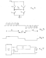
- the signal on the primary 3 comprises a plurality of pulses generated at an H-bridge circuit arrangement as shown in Figure 2 .
- This comprises four FET switches 5, 6, 7 and 8 connected between ground and a positive voltage supply at 9.
- FETs 5 and 7 are connected in series between the input 9 and ground as are FETs 6 and 8.
- the single turn primary 3 is connected at one end between FETs 5 and 7 and at its other end between FETs 6 and 8.
- each of the FETs 5 to 8 When the circuit is inactive, each of the FETs 5 to 8 is open as shown. When it is wished to switch on the main FET 2 in module 1, and corresponding FETs in the other modules, FETs 5 and 8 are closed. The input 9 is pulsed to give a series of positive pulses through the primary 3 as shown in period t1 in Figure 3 . When it is required to switch off the main FET 2 in module 1, following a reset period during which FETs 7 and 8 only for the H-bridge circuit of Figure 2 are closed, the switch configuration is changed so as to close FETs 6 and 7 and open FETs 5 and 8, changing the direction of current flow through the single primary 3 and giving a series of negative polarity pulses as shown in period t2 in Figure 3.
- Figure 3 shows the signals applied to the primary 3.
- the reset period t3 between period t1 and t2 although shown in Figure 3 as being relatively large compared to the pulse width may in reality be quite short. It is only necessary for it to be sufficiently long to reset the transformer 4.
- each pulse in the pulse trains illustrated in Figure 3 has a pulse width of 1 microsecond.
- the FETs 5 to 8 are switched by a control processor (not shown) so as to achieve the desired operation of the main FET 2 of module 1 and the other main FETs.
- the width and prf of the output and the rate of rise of the output to a load may be controlled.
- the test parameters including operating level, can be electronically controlled, making test selection and calibration very simple.
- the pulses as shown in Figure 3 are applied via the primary 3 to the toroidal transformer 4 in module 1. These pulses are used to provide a power supply to the driver 10 of the main FET 2.
- the ends of the secondary 4 are connected via diodes 11 and 12 at 13 and a central tap 14 is connected via a Zener diode 15 and capacitor 16 in parallel to give a power supply to the driver 10 on line 17.
- the control pulses applied via the single primary 3 also control the operation of the FET 2 enabling it to be switched off or on as required.
- the train of control pulses is applied via line 18 from one end of the secondary 4 via a diode 19 to the driver 10 of the main FET 2. This causes the FET 2 to remain switched on during the entire period that the train of pulses is applied to the driver 10.
- the negative pulses as shown in t2 of Figure 3 are applied to the single primary 3. These give a train control pulses on line 20 and the other end of the secondary 4 which are applied via another FET 21 to the driver 10. The FET 2 then remains switched off for as long as the pulses continue to be applied to the driver 10.
- Figure 4 shows the FET trigger signal produced from the pulse train illustrated in Figure 3 .
- the pulse repetition frequency and pulse length can be controlled over a very wide range.
- Figure 5 illustrates schematically a modulator incorporating the switching arrangement illustrated in Figure 1 and shown at 22. This is connected to a dc supply 23, load 24 and a reservoir capacitor 25. This arrangement permits the dc supply 23, the load 24 and capacitor 25 to have one terminal common to each, minimising the displacement current in the stray capacitance, and hence reducing loss and maximising switching speed.
Landscapes
- Engineering & Computer Science (AREA)
- Power Engineering (AREA)
- Dc-Dc Converters (AREA)
- Electronic Switches (AREA)
- Power Conversion In General (AREA)
Description
- This invention relates to switching arrangement and more particularly, but not exclusively, to a switching arrangement used in a pulse modulator for providing pulses of variable length and pulse repetition frequency (PRF).
- A requirement exists for pulse modulator test equipment which is suitable for supplying variable output, with operating voltages, of say up to 30 kV, duty cycles in the range of less than 1 % and up to greater than 30%, pulse widths in the range of 15ns to greater than 100 microseconds and PRFs up to 750 kHz. In conventional arrangements, a pulse transformer would be used as a modulator for driving rf sources. However, it would be difficult to design a pulse transformer which could meet the demanding requirements outlined above.
- The present invention seeks to provide a switching arrangement and particularly a switching arrangement suitable for driving rf sources for test purposes. However, it is envisaged that the arrangement may also be suitable for use in other non-test applications where demanding switching requirements exist.
- Switching arrangements for driving FETs via transformers are known ("HIGH PERFORMANCE MODULATORS USING MOSFETS", Power Modulator Symposium 1988, pages 34-38;
US-A-5 763 962 : andDE-A3 243 660 ) but, in each case, the FET is only on for the duration of the driving voltage pulse applied to the transformer. - The invention is defined in the claims to which reference is now directed.
- In an embodiment of a switching arrangement, by controlling the duration of the pulse train and it polarity, the switch can be controlled to give an output having characteristics which are variable over wide ranges, giving great versatility. For example, the PRF may be varied so as to give anything from a dc output to a frequency of 750 kHz. Providing pulses of one polarity continue to be applied, the switch will remain in its maintained state. The invention is thus particularly applicable for use in test equipment.
- In a preferred arrangement, the control pulses are used to supply power to the switch drive circuitry. Advantageously, the switch is a power FET.
- In a preferred arrangement, an H-bridge circuit is included to generate the control pulses, the H-bridge circuit including the primary winding of a transformer, and a secondary of the transformer being connected to the switch.
- In a particularly advantageous arrangement, a plurality of switches are included, each switch having a respective different secondary winding connected thereto and there being a common single primary. This enables the switches to be controlled and powered simultaneously with a single input.
- In an embodiment of the invention, a pulse modulator includes a switch arrangement in accordance with the invention, and in another feature of the invention, test equipment includes a pulse modulator including the switching arrangement also. The invention is particularly advantageously applicable to test equipment where it is often necessary to be able to produce a wide range of outputs having very different characteristics.
- One way in which the invention may be performed is now described by way of example with reference to the accompanying drawings in which:
-
Figure 1 is a schematic circuit diagram of a pulse modulator including a switching arrangement in accordance with the invention; -
Figure 2 is a schematic diagram of an H-bridge circuit used to produce pulses to be supplied to the arrangement shown inFigure 1 ; -
Figure 3 and 4 are pulse diagrams illustrating the operation of the arrangement ofFigure 1 ; and -
Figure 5 schematically shows a modulator circuit including a switching arrangement as shown inFigure 1 . - With reference to
Figure 1 , a switching arrangement comprises twenty identical modules, onemodule 1 being shown in greater detail. Themodule 1 includes a main FET 2 which is the main switching element, the main FET of each of the modules being connected in series with one another as indicated. The modules are arranged in a stack, this modular arrangement being particularly suitable for convection cooling with either air or fluid. - The power for the FET 2 and its control signals are supplied from an isolated single turn primary 3 which passes through a toroidal secondary transformer 4 included in the
module 1 and also through similar toroidal transformers included in each of the other modules. Thus the input supplied on the common single turn primary 3 is applied to each of the modules in parallel. - The signal on the primary 3 comprises a plurality of pulses generated at an H-bridge circuit arrangement as shown in
Figure 2 . This comprises fourFET switches FETs 5 and 7 are connected in series between the input 9 and ground as areFETs 6 and 8. The single turn primary 3 is connected at one end betweenFETs 5 and 7 and at its other end betweenFETs 6 and 8. - When the circuit is inactive, each of the
FETs 5 to 8 is open as shown. When it is wished to switch on the main FET 2 inmodule 1, and corresponding FETs in the other modules,FETs Figure 3 . When it is required to switch off the main FET 2 inmodule 1, following a reset period during whichFETs 7 and 8 only for the H-bridge circuit ofFigure 2 are closed, the switch configuration is changed so as to close FETs 6 and 7 and openFETs Figure 3. Figure 3 shows the signals applied to the primary 3. The reset period t3 between period t1 and t2 although shown inFigure 3 as being relatively large compared to the pulse width may in reality be quite short. It is only necessary for it to be sufficiently long to reset the transformer 4. Typically each pulse in the pulse trains illustrated inFigure 3 has a pulse width of 1 microsecond. TheFETs 5 to 8 are switched by a control processor (not shown) so as to achieve the desired operation of the main FET 2 ofmodule 1 and the other main FETs. Thus the width and prf of the output and the rate of rise of the output to a load may be controlled. Thus in test equipment, the test parameters, including operating level, can be electronically controlled, making test selection and calibration very simple. - With reference to
Figure 1 , the pulses as shown inFigure 3 are applied via the primary 3 to the toroidal transformer 4 inmodule 1. These pulses are used to provide a power supply to the driver 10 of the main FET 2. The ends of the secondary 4 are connected viadiodes central tap 14 is connected via a Zener diode 15 andcapacitor 16 in parallel to give a power supply to the driver 10 online 17. - The control pulses applied via the single primary 3 also control the operation of the FET 2 enabling it to be switched off or on as required. When the pulses have positive polarity, as shown at the time t1 in
Figure 3 , the train of control pulses is applied vialine 18 from one end of the secondary 4 via adiode 19 to the driver 10 of the main FET 2. This causes the FET 2 to remain switched on during the entire period that the train of pulses is applied to the driver 10. When the FET 2 is to be switched off, the negative pulses as shown in t2 ofFigure 3 are applied to the single primary 3. These give a train control pulses online 20 and the other end of the secondary 4 which are applied via another FET 21 to the driver 10. The FET 2 then remains switched off for as long as the pulses continue to be applied to the driver 10.Figure 4 shows the FET trigger signal produced from the pulse train illustrated inFigure 3 . - Thus, by varying the length and polarity of the pulse train, control of the switching of the main FET is accomplished. The pulse repetition frequency and pulse length can be controlled over a very wide range.
-
Figure 5 illustrates schematically a modulator incorporating the switching arrangement illustrated inFigure 1 and shown at 22. This is connected to adc supply 23,load 24 and areservoir capacitor 25. This arrangement permits thedc supply 23, theload 24 andcapacitor 25 to have one terminal common to each, minimising the displacement current in the stray capacitance, and hence reducing loss and maximising switching speed.
Claims (8)
- A switching arrangement comprising a solid state switch (2) and control means (3,4,10) arranged to apply a train of control pulses to the solid state switch, such that when pulses of one polarity are applied, the switch is maintained in an on state and when pulses of the other polarity are applied, the switch is maintained in an off state, the control means (3,4,10) including a transformer (3,4) having a primary (3) and secondary (4) arranged to apply the control pulses of each polarity from the secondary in response to pulses of respective polarity applied to the primary, wherein the solid state switch comprises a FET (2) which is arranged to remain switched on during the entire period that the train of pulses of the one polarity are applied and wherein the control pulses are used to supply power to a switch drive circuit (10-12), characterised in that the secondary (4) is centre-tapped, and the switch drive circuit (10-12) includes a driver (10) having its input coupled to one end of the secondary (4) via a diode (19), in order to supply the pulses of one polarity to the FET (2), and having its input coupled to a solid state switch (21) controlled from the other end of the secondary (4), in order to supply the pulses of the other polarity to the FET (2), and including charge storage means (16) coupled between the centre tap and diodes (11,12) connected to the respective ends of the secondary (4), to receive charge on both polarities of pulse.
- An arrangement as claimed in claim 1 wherein the switch is a power FET (2).
- An arrangement as claimed in claim 1 or 2 wherein the control means includes an H-bridge circuit (3, 5-8) to generate the control pulses, the circuit including the primary (3) of a transformer, the secondary (4) being connected to the switch.
- An arrangement as claimed in any preceding claim and including a plurality of solid state switches (2), each having a respective different secondary (4) connected thereto and a common single primary (3) transformer.
- An arrangement as claimed in claim 4 wherein the secondary windings are toroidal.
- An arrangement as claimed in claim 4 or 5 wherein the plurality of solid state switches (2) are connected in series.
- A pulse modulator including a switching arrangement as claimed in any preceding claim.
- A test arrangement including a pulse modulator as claimed in claim 7.
Applications Claiming Priority (2)
| Application Number | Priority Date | Filing Date | Title |
|---|---|---|---|
| GB9813382A GB2341288B (en) | 1998-06-23 | 1998-06-23 | Switching arrangement |
| GB9813382 | 1998-06-23 |
Publications (3)
| Publication Number | Publication Date |
|---|---|
| EP0967722A2 EP0967722A2 (en) | 1999-12-29 |
| EP0967722A3 EP0967722A3 (en) | 2000-07-12 |
| EP0967722B1 true EP0967722B1 (en) | 2010-11-17 |
Family
ID=10834127
Family Applications (1)
| Application Number | Title | Priority Date | Filing Date |
|---|---|---|---|
| EP99304899A Expired - Lifetime EP0967722B1 (en) | 1998-06-23 | 1999-06-22 | Switching arrangement |
Country Status (4)
| Country | Link |
|---|---|
| US (1) | US6496047B1 (en) |
| EP (1) | EP0967722B1 (en) |
| DE (1) | DE69942942D1 (en) |
| GB (1) | GB2341288B (en) |
Families Citing this family (40)
| Publication number | Priority date | Publication date | Assignee | Title |
|---|---|---|---|---|
| GB2356753B (en) * | 1999-11-29 | 2004-08-11 | Eev Ltd | Switching arrangement |
| US6900557B1 (en) * | 2000-01-10 | 2005-05-31 | Diversified Technologies, Inc. | High power modulator |
| DE10146900A1 (en) * | 2001-09-24 | 2003-04-10 | Abb Research Ltd | Circuit arrangement for voltage-isolated control of series semiconducting switch elements has secondary stage producing positive and negative pulses for switch-on and switch-off phases |
| JP4082672B2 (en) * | 2003-03-06 | 2008-04-30 | 株式会社デンソー | Electrically isolated switching element drive circuit |
| US8253474B2 (en) * | 2011-01-25 | 2012-08-28 | Advantest Corporation | Leakage compensated electronic switch |
| BR112013026936A2 (en) * | 2011-04-21 | 2016-12-27 | Ge Energy Power Conversion Technology Ltd | drive circuit and drive method |
| WO2013075737A1 (en) * | 2011-11-22 | 2013-05-30 | Abb Technology Ag | Intelligent gate driver for igbt |
| EP3041139B1 (en) * | 2013-08-27 | 2018-10-10 | Panasonic Intellectual Property Management Co., Ltd. | Gate driving circuit |
| US11539352B2 (en) | 2013-11-14 | 2022-12-27 | Eagle Harbor Technologies, Inc. | Transformer resonant converter |
| US10978955B2 (en) | 2014-02-28 | 2021-04-13 | Eagle Harbor Technologies, Inc. | Nanosecond pulser bias compensation |
| US10020800B2 (en) | 2013-11-14 | 2018-07-10 | Eagle Harbor Technologies, Inc. | High voltage nanosecond pulser with variable pulse width and pulse repetition frequency |
| US10892140B2 (en) | 2018-07-27 | 2021-01-12 | Eagle Harbor Technologies, Inc. | Nanosecond pulser bias compensation |
| CN109873621B (en) | 2013-11-14 | 2023-06-16 | 鹰港科技有限公司 | High-voltage nanosecond pulse generator |
| US10483089B2 (en) | 2014-02-28 | 2019-11-19 | Eagle Harbor Technologies, Inc. | High voltage resistive output stage circuit |
| US11004660B2 (en) | 2018-11-30 | 2021-05-11 | Eagle Harbor Technologies, Inc. | Variable output impedance RF generator |
| US11430635B2 (en) | 2018-07-27 | 2022-08-30 | Eagle Harbor Technologies, Inc. | Precise plasma control system |
| US9966837B1 (en) | 2016-07-08 | 2018-05-08 | Vpt, Inc. | Power converter with circuits for providing gate driving |
| KR101806731B1 (en) * | 2016-08-17 | 2017-12-08 | 현대자동차주식회사 | Gate driving apparatus |
| FR3057722B1 (en) | 2016-10-18 | 2018-11-30 | Thales | DEVICE FOR CONTROLLING A TRANSISTOR |
| GB2559423B8 (en) * | 2017-02-07 | 2023-06-28 | Heyday Integrated Circuits Sas | An isolated high side drive circuit |
| EP4266579A3 (en) | 2017-02-07 | 2023-12-27 | Eagle Harbor Technologies, Inc. | Transformer resonant converter |
| EP3665775B1 (en) | 2017-08-25 | 2025-08-20 | Eagle Harbor Technologies, Inc. | Arbitrary waveform generation using nanosecond pulses |
| GB2567227A (en) | 2017-10-06 | 2019-04-10 | Heyday Integrated Circuits | Galvanically isolated gate drive circuit with power transfer |
| US11302518B2 (en) | 2018-07-27 | 2022-04-12 | Eagle Harbor Technologies, Inc. | Efficient energy recovery in a nanosecond pulser circuit |
| US11222767B2 (en) | 2018-07-27 | 2022-01-11 | Eagle Harbor Technologies, Inc. | Nanosecond pulser bias compensation |
| US11810761B2 (en) | 2018-07-27 | 2023-11-07 | Eagle Harbor Technologies, Inc. | Nanosecond pulser ADC system |
| US11532457B2 (en) | 2018-07-27 | 2022-12-20 | Eagle Harbor Technologies, Inc. | Precise plasma control system |
| KR102499709B1 (en) | 2018-08-10 | 2023-02-16 | 이글 하버 테크놀로지스, 인코포레이티드 | Plasma sheath control for RF plasma reactors |
| US12456604B2 (en) | 2019-12-24 | 2025-10-28 | Eagle Harbor Technologies, Inc. | Nanosecond pulser RF isolation for plasma systems |
| KR20240028538A (en) | 2019-01-08 | 2024-03-05 | 이글 하버 테크놀로지스, 인코포레이티드 | Efficient energy recovery in a nanosecond pulser circuit |
| US10812069B1 (en) | 2019-08-06 | 2020-10-20 | Baker Hughes, A Ge Company, Llc | Isolated switch driving circuit |
| TWI778449B (en) | 2019-11-15 | 2022-09-21 | 美商鷹港科技股份有限公司 | High voltage pulsing circuit |
| KR20230150396A (en) | 2019-12-24 | 2023-10-30 | 이글 하버 테크놀로지스, 인코포레이티드 | Nanosecond pulser rf isolation for plasma systems |
| US11967484B2 (en) | 2020-07-09 | 2024-04-23 | Eagle Harbor Technologies, Inc. | Ion current droop compensation |
| US11824542B1 (en) | 2022-06-29 | 2023-11-21 | Eagle Harbor Technologies, Inc. | Bipolar high voltage pulser |
| CN119998919A (en) | 2022-09-29 | 2025-05-13 | 鹰港科技有限公司 | High pressure plasma control |
| US12543574B2 (en) | 2023-04-14 | 2026-02-03 | Allegro Microsystems, Llc | Voltage-isolated integrated circuit packages |
| US12557668B2 (en) | 2023-04-27 | 2026-02-17 | Allegro Microsystems, Llc | High voltage integrated circuit packages with diagonalized lead configuration and method of making the same |
| US12267071B2 (en) | 2023-06-01 | 2025-04-01 | Allegro Microsystems, Llc | Desaturation circuit having temperature compensation |
| US12526012B1 (en) | 2024-09-26 | 2026-01-13 | Allegro Microsystems, Llc | Wireless power transmission with channel redundancy |
Family Cites Families (22)
| Publication number | Priority date | Publication date | Assignee | Title |
|---|---|---|---|---|
| US4038568A (en) * | 1976-02-23 | 1977-07-26 | The United States Of America As Represented By The Secretary Of The Air Force | Pulse peak sample and hold circuit |
| US4425518A (en) * | 1981-03-25 | 1984-01-10 | The United States Of America As Represented By The Secretary Of The Air Force | High voltage field effect transistor pulse apparatus |
| AT377138B (en) * | 1981-11-26 | 1985-02-11 | Zumtobel Ag | CIRCUIT ARRANGEMENT FOR POTENTIALLY SEPARATE CONTROLLING AT LEAST ONE FIELD EFFECT TRANSISTOR |
| US4511815A (en) * | 1983-08-15 | 1985-04-16 | International Rectifier Corporation | Transformer-isolated power MOSFET driver circuit |
| FR2556905B1 (en) * | 1983-12-14 | 1989-07-13 | Europ Agence Spatiale | CONTROL CIRCUIT FOR POWER FIELD EFFECT TRANSISTOR |
| US4577166A (en) * | 1984-08-22 | 1986-03-18 | The United States Of America As Represented By The Secretary Of The Air Force | Miniature high performance pulsed modulator apparatus |
| FR2583235B1 (en) * | 1985-06-11 | 1992-11-27 | Inf Milit Spatiale Aeronaut | MINIATURIZED DEVICE FOR TRANSMITTING BINARY INFORMATION BY PULSE TRANSFORMER WITH CONTINUOUS COMPONENT RECONSTRUCTION |
| JPS63133819A (en) * | 1986-11-11 | 1988-06-06 | シーメンス、アクチエンゲゼルシヤフト | Circuit device of self-protecting power switch |
| US4774419A (en) * | 1987-06-24 | 1988-09-27 | General Electric Company | Transformer coupled drive circuit |
| US4937470A (en) * | 1988-05-23 | 1990-06-26 | Zeiler Kenneth T | Driver circuit for power transistors |
| EP0472318A3 (en) * | 1990-08-06 | 1994-08-10 | At & T Corp | Led pulse shaping circuit |
| US5304863A (en) * | 1991-08-30 | 1994-04-19 | Hughes Aircraft Company | Transformer driver having unlimited duty cycle capability by inserting narrow pulses during unlimited duty cycles |
| FR2684500B1 (en) * | 1991-12-02 | 1994-06-10 | Rahban Thierry | BIPOLAR GENERATOR WITH SWITCHABLE POLARITY GALVANIC INSULATION. |
| US5276357A (en) * | 1992-09-01 | 1994-01-04 | Broadcast Electronics, Inc. | High efficiency quasi-square wave drive circuit for switching power amplifiers |
| US5741303A (en) * | 1993-09-13 | 1998-04-21 | Angeion Corp | Electrode back-charging pre-treatment system for an implantable cardioverter defibrillator |
| FR2730108A1 (en) * | 1995-01-26 | 1996-08-02 | Commissariat Energie Atomique | SWITCHING DEVICE FOR A HIGH VOLTAGE CIRCUIT WITH A PULSE TRANSFORMER |
| US5594378A (en) * | 1995-04-13 | 1997-01-14 | Kruse; Neils A. | Fast high voltage modulator circuit |
| JPH0993908A (en) * | 1995-09-22 | 1997-04-04 | Denshi Seigyo Group:Kk | Semiconductor switch drive circuit |
| US5684426A (en) * | 1995-12-21 | 1997-11-04 | General Electric Company | GTO gate driver circuits for snubbered and zero voltage soft switching converters |
| FR2743222B1 (en) * | 1995-12-27 | 1998-02-13 | Commissariat Energie Atomique | PULSE POWER SWITCH CAPABLE OF PROVIDING LOW CURRENT HIGH LOW CURRENT PULSES |
| US5913877A (en) * | 1996-03-11 | 1999-06-22 | Kroll; Mark W. | Implantable defibrillator system for generating a biphasic waveform with enhanced phase transition |
| US5859519A (en) * | 1997-05-29 | 1999-01-12 | General Electric Company | Single phase motor drive |
-
1998
- 1998-06-23 GB GB9813382A patent/GB2341288B/en not_active Expired - Lifetime
-
1999
- 1999-06-22 DE DE69942942T patent/DE69942942D1/en not_active Expired - Lifetime
- 1999-06-22 EP EP99304899A patent/EP0967722B1/en not_active Expired - Lifetime
- 1999-06-23 US US09/339,021 patent/US6496047B1/en not_active Expired - Lifetime
Also Published As
| Publication number | Publication date |
|---|---|
| GB9813382D0 (en) | 1998-08-19 |
| EP0967722A2 (en) | 1999-12-29 |
| EP0967722A3 (en) | 2000-07-12 |
| GB2341288B (en) | 2003-12-10 |
| DE69942942D1 (en) | 2010-12-30 |
| US6496047B1 (en) | 2002-12-17 |
| GB2341288A (en) | 2000-03-08 |
Similar Documents
| Publication | Publication Date | Title |
|---|---|---|
| US6496047B1 (en) | Solid state switch with pulsed control | |
| US5895984A (en) | Circuit arrangement for feeding a pulse output stage | |
| EP0360854B1 (en) | Two-state, bilateral, single-pole, double-throw, half-bridge power-switching apparatus and power supply means for such electronic power switching apparatus | |
| EP1131853B1 (en) | Driver for piezoelectric motors | |
| KR870011315A (en) | Drive signal generator | |
| KR100231653B1 (en) | MOSFET switch matrix | |
| US6900557B1 (en) | High power modulator | |
| WO2015016891A1 (en) | Isolated uni-polar transistor gate drive | |
| EP0420518B1 (en) | Power saving drive circuit for TFEL devices | |
| US5461532A (en) | Electronic pulse transformer | |
| US8023296B2 (en) | High voltage, high speed, high pulse repetition rate pulse generator | |
| US7072196B1 (en) | Multi-stage high voltage solid state switch | |
| US7200012B1 (en) | Circuit utilizing a push-pull pulse width modulator to control a full-bridge inverter | |
| US6462605B1 (en) | Low-jitter high-power thyristor array pulse driver and generator | |
| KR102573440B1 (en) | Pulse power supply and high-speed gate control method thereof | |
| CA2087885A1 (en) | Halftone image device and its driving circuit | |
| KR102616237B1 (en) | Pulse power supply | |
| KR101718337B1 (en) | Pulse power supply apparatus for providing bi-directional high voltage pulse | |
| JP3445721B2 (en) | Positive and negative pulse type high voltage power supply | |
| US5434528A (en) | Gate drive using continuous alternating power and a diode H-bridge | |
| Burkhart et al. | Inductive Adders | |
| JP4679176B2 (en) | Pulse modulation circuit | |
| SU551787A1 (en) | Device for controlling two-phase asynchronous electric motor | |
| SU1661934A1 (en) | Generator of pulses for controlling converter thyristors | |
| JPH0879024A (en) | Pulse modulator |
Legal Events
| Date | Code | Title | Description |
|---|---|---|---|
| PUAI | Public reference made under article 153(3) epc to a published international application that has entered the european phase |
Free format text: ORIGINAL CODE: 0009012 |
|
| AK | Designated contracting states |
Kind code of ref document: A2 Designated state(s): BE DE FR IT NL SE |
|
| AX | Request for extension of the european patent |
Free format text: AL;LT;LV;MK;RO;SI |
|
| PUAL | Search report despatched |
Free format text: ORIGINAL CODE: 0009013 |
|
| AK | Designated contracting states |
Kind code of ref document: A3 Designated state(s): AT BE CH CY DE DK ES FI FR GB GR IE IT LI LU MC NL PT SE |
|
| AX | Request for extension of the european patent |
Free format text: AL;LT;LV;MK;RO;SI |
|
| 17P | Request for examination filed |
Effective date: 20010112 |
|
| AKX | Designation fees paid | ||
| RBV | Designated contracting states (corrected) |
Designated state(s): BE DE FR IT NL SE |
|
| RAP1 | Party data changed (applicant data changed or rights of an application transferred) |
Owner name: E2V TECHNOLOGIES (UK) LIMITED |
|
| 17Q | First examination report despatched |
Effective date: 20061103 |
|
| GRAP | Despatch of communication of intention to grant a patent |
Free format text: ORIGINAL CODE: EPIDOSNIGR1 |
|
| GRAS | Grant fee paid |
Free format text: ORIGINAL CODE: EPIDOSNIGR3 |
|
| GRAA | (expected) grant |
Free format text: ORIGINAL CODE: 0009210 |
|
| AK | Designated contracting states |
Kind code of ref document: B1 Designated state(s): BE DE FR IT NL SE |
|
| REF | Corresponds to: |
Ref document number: 69942942 Country of ref document: DE Date of ref document: 20101230 Kind code of ref document: P |
|
| REG | Reference to a national code |
Ref country code: NL Ref legal event code: T3 |
|
| REG | Reference to a national code |
Ref country code: SE Ref legal event code: TRGR |
|
| PLBE | No opposition filed within time limit |
Free format text: ORIGINAL CODE: 0009261 |
|
| STAA | Information on the status of an ep patent application or granted ep patent |
Free format text: STATUS: NO OPPOSITION FILED WITHIN TIME LIMIT |
|
| 26N | No opposition filed |
Effective date: 20110818 |
|
| REG | Reference to a national code |
Ref country code: DE Ref legal event code: R097 Ref document number: 69942942 Country of ref document: DE Effective date: 20110818 |
|
| REG | Reference to a national code |
Ref country code: FR Ref legal event code: PLFP Year of fee payment: 18 |
|
| REG | Reference to a national code |
Ref country code: FR Ref legal event code: PLFP Year of fee payment: 19 |
|
| REG | Reference to a national code |
Ref country code: DE Ref legal event code: R082 Ref document number: 69942942 Country of ref document: DE Representative=s name: MANITZ FINSTERWALD PATENT- UND RECHTSANWALTSPA, DE Ref country code: DE Ref legal event code: R082 Ref document number: 69942942 Country of ref document: DE Representative=s name: MANITZ FINSTERWALD PATENTANWAELTE PARTMBB, DE Ref country code: DE Ref legal event code: R081 Ref document number: 69942942 Country of ref document: DE Owner name: TELEDYNE E2V (UK) LTD., CHELMSFORD, GB Free format text: FORMER OWNER: E2V TECHNOLOGIES (UK) LTD., CHELMSFORD, ESSEX, GB |
|
| REG | Reference to a national code |
Ref country code: NL Ref legal event code: HC Owner name: TELEDYNE E2V (UK) LIMITED; GB Free format text: DETAILS ASSIGNMENT: CHANGE OF OWNER(S), CHANGE OF OWNER(S) NAME; FORMER OWNER NAME: E2V TECHNOLOGIES (UK) LIMITED Effective date: 20171208 |
|
| REG | Reference to a national code |
Ref country code: BE Ref legal event code: HC Owner name: TELEDYNE E2V (UK) LIMITED; GB Free format text: DETAILS ASSIGNMENT: CHANGE OF OWNER(S), CHANGEMENT DE NOM DU PROPRIETAIRE; FORMER OWNER NAME: E2V TECHNOLOGIES (UK) LIMITED Effective date: 20171213 |
|
| REG | Reference to a national code |
Ref country code: FR Ref legal event code: CD Owner name: TELEDYNE E2V (UK) LIMITED, GB Effective date: 20180410 |
|
| REG | Reference to a national code |
Ref country code: FR Ref legal event code: PLFP Year of fee payment: 20 |
|
| PGFP | Annual fee paid to national office [announced via postgrant information from national office to epo] |
Ref country code: NL Payment date: 20180626 Year of fee payment: 20 |
|
| PGFP | Annual fee paid to national office [announced via postgrant information from national office to epo] |
Ref country code: FR Payment date: 20180626 Year of fee payment: 20 Ref country code: BE Payment date: 20180627 Year of fee payment: 20 |
|
| PGFP | Annual fee paid to national office [announced via postgrant information from national office to epo] |
Ref country code: SE Payment date: 20180627 Year of fee payment: 20 |
|
| PGFP | Annual fee paid to national office [announced via postgrant information from national office to epo] |
Ref country code: DE Payment date: 20180627 Year of fee payment: 20 Ref country code: IT Payment date: 20180621 Year of fee payment: 20 |
|
| REG | Reference to a national code |
Ref country code: DE Ref legal event code: R071 Ref document number: 69942942 Country of ref document: DE |
|
| REG | Reference to a national code |
Ref country code: NL Ref legal event code: MK Effective date: 20190621 |
|
| REG | Reference to a national code |
Ref country code: BE Ref legal event code: MK Effective date: 20190622 |
|
| REG | Reference to a national code |
Ref country code: SE Ref legal event code: EUG |