EP0966819B1 - Phase-locked loop with continuously adjustable bandwith - Google Patents
Phase-locked loop with continuously adjustable bandwith Download PDFInfo
- Publication number
- EP0966819B1 EP0966819B1 EP98910290A EP98910290A EP0966819B1 EP 0966819 B1 EP0966819 B1 EP 0966819B1 EP 98910290 A EP98910290 A EP 98910290A EP 98910290 A EP98910290 A EP 98910290A EP 0966819 B1 EP0966819 B1 EP 0966819B1
- Authority
- EP
- European Patent Office
- Prior art keywords
- phase
- signal
- information signal
- bandwidth
- corrected information
- Prior art date
- Legal status (The legal status is an assumption and is not a legal conclusion. Google has not performed a legal analysis and makes no representation as to the accuracy of the status listed.)
- Expired - Lifetime
Links
Images


Classifications
-
- H—ELECTRICITY
- H04—ELECTRIC COMMUNICATION TECHNIQUE
- H04B—TRANSMISSION
- H04B1/00—Details of transmission systems, not covered by a single one of groups H04B3/00 - H04B13/00; Details of transmission systems not characterised by the medium used for transmission
- H04B1/69—Spread spectrum techniques
- H04B1/707—Spread spectrum techniques using direct sequence modulation
- H04B1/7073—Synchronisation aspects
- H04B1/7085—Synchronisation aspects using a code tracking loop, e.g. a delay-locked loop
-
- H—ELECTRICITY
- H04—ELECTRIC COMMUNICATION TECHNIQUE
- H04B—TRANSMISSION
- H04B1/00—Details of transmission systems, not covered by a single one of groups H04B3/00 - H04B13/00; Details of transmission systems not characterised by the medium used for transmission
- H04B1/69—Spread spectrum techniques
- H04B1/707—Spread spectrum techniques using direct sequence modulation
-
- H—ELECTRICITY
- H04—ELECTRIC COMMUNICATION TECHNIQUE
- H04L—TRANSMISSION OF DIGITAL INFORMATION, e.g. TELEGRAPHIC COMMUNICATION
- H04L27/00—Modulated-carrier systems
- H04L27/0014—Carrier regulation
-
- H—ELECTRICITY
- H04—ELECTRIC COMMUNICATION TECHNIQUE
- H04L—TRANSMISSION OF DIGITAL INFORMATION, e.g. TELEGRAPHIC COMMUNICATION
- H04L27/00—Modulated-carrier systems
- H04L27/18—Phase-modulated carrier systems, i.e. using phase-shift keying
- H04L27/22—Demodulator circuits; Receiver circuits
- H04L27/233—Demodulator circuits; Receiver circuits using non-coherent demodulation
- H04L27/2332—Demodulator circuits; Receiver circuits using non-coherent demodulation using a non-coherent carrier
-
- H—ELECTRICITY
- H04—ELECTRIC COMMUNICATION TECHNIQUE
- H04B—TRANSMISSION
- H04B1/00—Details of transmission systems, not covered by a single one of groups H04B3/00 - H04B13/00; Details of transmission systems not characterised by the medium used for transmission
- H04B1/69—Spread spectrum techniques
- H04B1/707—Spread spectrum techniques using direct sequence modulation
- H04B1/7097—Interference-related aspects
- H04B1/711—Interference-related aspects the interference being multi-path interference
- H04B1/7115—Constructive combining of multi-path signals, i.e. RAKE receivers
- H04B1/7117—Selection, re-selection, allocation or re-allocation of paths to fingers, e.g. timing offset control of allocated fingers
-
- H—ELECTRICITY
- H04—ELECTRIC COMMUNICATION TECHNIQUE
- H04L—TRANSMISSION OF DIGITAL INFORMATION, e.g. TELEGRAPHIC COMMUNICATION
- H04L27/00—Modulated-carrier systems
- H04L27/0014—Carrier regulation
- H04L2027/0044—Control loops for carrier regulation
- H04L2027/0053—Closed loops
-
- H—ELECTRICITY
- H04—ELECTRIC COMMUNICATION TECHNIQUE
- H04L—TRANSMISSION OF DIGITAL INFORMATION, e.g. TELEGRAPHIC COMMUNICATION
- H04L27/00—Modulated-carrier systems
- H04L27/0014—Carrier regulation
- H04L2027/0044—Control loops for carrier regulation
- H04L2027/0053—Closed loops
- H04L2027/0055—Closed loops single phase
-
- H—ELECTRICITY
- H04—ELECTRIC COMMUNICATION TECHNIQUE
- H04L—TRANSMISSION OF DIGITAL INFORMATION, e.g. TELEGRAPHIC COMMUNICATION
- H04L27/00—Modulated-carrier systems
- H04L27/0014—Carrier regulation
- H04L2027/0044—Control loops for carrier regulation
- H04L2027/0063—Elements of loops
- H04L2027/0069—Loop filters
-
- H—ELECTRICITY
- H04—ELECTRIC COMMUNICATION TECHNIQUE
- H04L—TRANSMISSION OF DIGITAL INFORMATION, e.g. TELEGRAPHIC COMMUNICATION
- H04L27/00—Modulated-carrier systems
- H04L27/0014—Carrier regulation
- H04L2027/0044—Control loops for carrier regulation
- H04L2027/0071—Control of loops
- H04L2027/0079—Switching between loops
- H04L2027/0081—Switching between loops between loops of different bandwidths
Definitions
- This invention is generally directed to wireless digital communication systems. More particularly, the invention is directed to a code division multiple access (CDMA) receiver having a continuously adjustable bandwidth phase-locked loop for accurately determining the carrier frequency of a received signal.
- CDMA code division multiple access
- B-CDMATM Broadband Code Division Multiple Access
- the spread signal is upconverted to an RF signal for transmission.
- a receiver having the same pseudorandom spreading code, receives the transmitted RF signal and mixes the received signal with an RF sinusoidal signal generated at the receiver by a first-stage local oscillator (LO) to downconvert the spread spectrum signal.
- the spreaded information signal is subsequently mixed with the pseudorandom spreading code, which has also been locally generated, to obtain the original information signal.
- a receiver In order to detect the information embedded in a received signal, a receiver must know the exact pseudorandom spreading code that was used to spread the signal. All signals which are not encoded with the pseudorandum code of the receiver appear as background noise to the receiver. Accordingly, as the number of users that are communicating within the operating range of a particular base station increases, the amount of background noise also increases, making it difficult for receivers to properly detect and receive signals.
- the transmitter may increase the power of the transmitted signal, but this will increase the noise as seen by other receivers. Therefore, increasing the signal-to-noise ratio of a received signal without requiring a corresponding increase in the transmission power of the signal is desirable.
- One way to increase the signal-to-noise ratio of a received signal is to ensure that the first stage local oscillator (LO) at the receiver is at the same frequency as the received RF carrier signal. If there is a slight frequency offset, the offset will manifest itself in the baseband section of the receiver as a phase error on the decoded QPSK symbol, resulting in a degradation of the quality of the communication.
- LO local oscillator
- the invention provides a system according to claim 1 and a method according to claim 10.
- the continuously adjusted-bandwidth phase-locked loop (PLL) of the present invention is used by a B-CDMATM receiver to correct for any deviation, or offset, that may exist between the received radio frequency (RF) carrier signal and the frequency of the first stage LO that converts the received RF carrier signal to an intermediate frequency (IF).
- the PLL in the receiver includes a filter with an adjustable bandwidth. A wider bandwidth is used during initial acquisition of the received signal. After the PLL has acquired the received carrier signal using the wider bandwidth, the bandwidth of the filter is gradually narrowed to provide a low steady-state error. Accordingly, it is an object of the invention to provide an improved CDMA receiver which corrects for any offset that may exist between the received RF carrier signal and the frequency of the first stage LO.
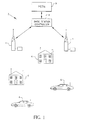
- a communication network 2 embodying the present invention is shown in Figure 1.
- the communication network 2 generally comprises one or more base stations 4 , each of which is in wireless communication with a plurality of subscriber units 6 , which may be fixed or mobile. Each subscriber unit 6 communicates with either the closest base station 4 or the base station 4 which provides the strongest communication signal.
- the base stations 4 also communicate with a base station controller 8 , which coordinates communications among base stations 4 .
- the communication network 2 may also be connected to a public switched telephone network (PSTN) 9 , wherein the base station controller 8 also coordinates communications between the base stations 4 and the PSTN 9 .
- PSTN public switched telephone network
- each base station 4 communicates with the base station controller 8 over a wireless link, although a land line may also be provided. A land line is particularly applicable when a base station 4 is in close proximity to the base station controller 8 .
- the base station controller 8 performs several functions. Primarily, the base station controller 8 provides all of the operations, administrative and maintenance (OA&M) signaling associated with establishing and maintaining all of the wireless communications between the subscriber units 6 , the base stations 4 , and the base station controller 8 .
- the base station controller 8 also provides an interface between the wireless communication system 2 and the PSTN 9 . This interface includes multiplexing and demultiplexing of the communication signals that enter and leave the system 2 via the base station controller 8 .
- the wireless communication system 2 is shown employing antennas to transmit RF signals, one skilled in the art should recognize that communications may be accomplished via microwave or satellite uplinks. Additionally, the functions of the base station controller 8 may be combined with a base station 4 to form a "master base station".
- a two-way communication channel 11 comprises a signal transmitted 13 (Tx) from the base station 4 to the subscriber unit 6 and a signal received 15 (Rx) by the base station 4 from the subscriber unit 6.
- the signaling between the base station 4 and the subscriber units 6 includes the transmission of a pilot signal 17.
- the pilot signal 17 is a spreading code which carries no data bits.
- the pilot signal 17 is used for subscriber unit 6 acquisition and synchronization, as well as for determining the parameters of the adaptive matched filter used in the data receiver.
- the subscriber unit 6 must acquire the pilot signal 17 transmitted by the base station 4 before it can receive or transmit any data. Acquisition is the process whereby the subscriber unit 6 aligns its locally generated spreading code with the received pilot signal 17 . The subscriber unit 6 searches through all of the possible phases of the received pilot signal 17 until it detects the correct phase, (the beginning of the pilot signal 17 ).
- the PLL 10 in accordance with the present invention acts upon the transmitted pilot signal 17 , which is an auxiliary signal transmitted from the base station 4 to all subscriber units 6 and from subscriber units 6 to the base station 4 which is not used as a traffic channel to transmit any voice or data information.
- the signal 17 is used: 1) to provide synchronization of the locally generated pseudorandom code with the transmitted pseudorandom code; and 2) as a transmission power reference during initial power ramp-up of the subscriber unit 6 .
- the pilot signal 17 is utilized to provide synchronization of the locally generated pseudorandom code with the transmitted pseudorandom code.
- the pilot signal 17 is additionally used in both the base station 4 and the subscriber unit 6 to determine the difference between the frequency of the received RF carrier signal and the first stage LO that downconverts the received RF carrier signal to IF.
- the CDMA pilot signal 17 is a sequence of pseudorandom complex numbers which are modulated by a constant complex pilot value having a magnitude of one and phase of zero.
- the advantage of using the pilot signal 17 is that the transmitted despread value is known to the subscriber unit 6 . This can be used by the PLL 10 in the subscriber unit 6 to estimate and correct for phase error due to RF carrier signal offset.
- the difference in the frequency of the received RF carrier signal and the first stage LO can be generally attributed to two sources: 1) component mismatches; and 2)RF distortion.
- Component mismatches between the transmitter oscillator 4 and the receiver oscillator 6 may cause slightly different oscillator outputs. These component mismatches can be further exacerbated by local environmental conditions, such as the heating or cooling of electronic components, which may cause performance changes in the components.
- RF distortion doppler effects caused by the motion of the subscriber unit 6 , the base station 4 or a multipath reflector may cause the RF carrier to become distorted during transmission. This may result in a RF carrier offset.
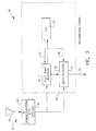
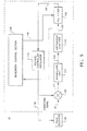
- the PLL 10 is implemented in a programmable digital signal processor within the digital receiver section 20 to provide flexibility in system architecture.
- the pilot signal 17 is received via the antenna 60 and is processed by the analog receiver section 61 , which includes an RF downconverter 63 and an analog-to-digital section 65 .
- the downconverted and digtized pilot signal 17 is then processed by the digital receiver section 20 which includes a pilot rake receiver 40, the PLL 10 , and a data receiver 42.
- the pilot signal 17 enters the rake receiver 40 for despreading.
- the PLL monitors the output from the pilot rake receiver 40, which comprises the despread pilot signal 30 , to estimate and correct for a phase error due to RF carrier offset, thereby providing acceptable speech quality.
- the pilot rake receiver 40 operates on the pilot signal 17 to build a receiver filter.
- the receiver filter compensates for channel distortion due to multipath effects.
- the filter parameters 45 are forwarded from the pilot rake receiver 40 to the data receiver 42 which constructs the receiver filter in accordance with those parameters 45. Accordingly, when a data signal enters the data receiver 42 , the data receiver 42 is able to compensate for channel distortion due to multipath effects and output a more accurate information signal 44 .
- the rake receiver 40 is shown in greater detail in Figure 4 .
- the rake receiver 40 provides an estimate of the complex impulse response, having real and imaginary components, of the channel over which the pilot signal 17 is transmitted.
- the rake receiver 40 has a plurality of independent rake elements 80.1, 80.2, 80.i, wherein the input to each rake element 80.1, 80.2, 80.i is a delayed and despread replica 100 of the received pilot signal 17 .
- the amount of delay 84 between adjacent rake elements 80.1, 80.2, 80.i is one chip.
- the delayed replicas 100 of the pilot signal 17 are created without delay lines by using a mixer 88, 90, 92 to correlate the received pilot signal 17 with the locally generated pilot pseudonoise code 86 , offset by the appropriate amount of chips 84 .
- the rake receiver 40 produces N noisy estimates of the sampled impulse response of the channel of the received pilot signal 17, at evenly spaced intervals, where N is the number of rake elements 80.1, 80.2, 80.i .
- the low pass filter on each rake element 80.1, 80.2, 80.i smooths each corresponding sample impulse response estimate.
- the complex conjugates of each smoothed sampled impulse response estimate are used as the weights on the channel-matching filter. This serves to remove the signal distortion from the received pilot signal 17 and data signals 46 that occur due to multipath effects in the channel.
- the pilot rake receiver 40 and the PLL 10 operate in conjunction with one another in the receiver section 20.
- the PLL 10 requires a despread pilot signal 30 with the distortion effects due to multipath removed. This is accomplished by the adaptive matched filter obtained from using the channel-impulse-response estimate provided by the pilot rake receiver 40 .
- the pilot rake receiver 40 and the data receiver 42 cannot operate effectively unless the received pilot signal 17 and the data signals 16 have been corrected for phase error due to RF carrier signal offset.
- the phase error correction signal 50 is provided by the PLL 10 to the pilot rake receiver 40 and data receiver 42. Optimal performance of the receiver 20 will not occur until the pilot rake receiver 40 and the PLL 10 have reached a mutually satisfactory equilibrium point.
- the operation of the data receiver 42 is well known to those of skill in the art.
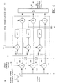
- the PLL 10 comprises a mixer 110 , a normalizing unit 112 , an arctangent analyzer 114 , a PLL filter 116 , a voltage controlled oscillator (VCO) 118 , and a bandwidth control section 120 .
- the mixer 110 receives its input from the pilot rake receiver 40.
- the signal output from the rake receiver 40 is the despread pilot signal 30 which has been processed to correct channel distortion due to multipath effects. This signal 30 is mixed with a "correction signal" 50 to produce a complex error signal 122.
- the bandwidth of the PLL filter 116 is adjusted by the bandwidth control section 120 to provide a revised correction signal 50 to the mixer 110 , the rake receiver 40 , and the data receiver 42 . This process is repeated until the complex error signal 122 output from the mixer 122 is at a minimum. It is desired to have the complex error signal 122 as small as possible; ideally it should be zero.
- the despread pilot signal 17 is a known complex number that has zero phase.
- This complex number can be represented in two forms as shown in Figure 6: 1) Cartesian form; and 2) polar form.
- Cartesian form the real part is referred to as the in-phase component, (I-component), and the imaginary part is referred to as the quadrature component, (Q-component).
- the complex error signal 122 is processed by the normalizing unit 112, which will be described in greater detail hereinafter.
- the normalized signal 124 is then input into the arctangent analyzer 114.
- the arctangent analyzer 114 analyzes the normalized signal 124 , which is in Cartesian coordinate form, using an 8I-by-8Q arctangent processor to determine the phase ⁇ of the complex number.
- the arctangent analyzer 114 uses the Cartesian I and Q components which are mapped to provide the phase ⁇ of the complex number.
- the size and complexity of lookup table 152 implemented within the arctangent analyzer 114 grows as the range of the values input into the arctangent analyzer 114 increases. Thus, if a wide range of values is permitted to be input into the arctangent analyzer 114 , the arctangent function increases in complexity and the lookup table 152 dramatically increases in size. Accordingly, in order to keep the implementation as simple as possible, the complex error signal 122 is normalized by the normalizing unit 112 prior to being input into the arctangent analyzer 114. The normalizing unit 112 receives the complex error signal 122 from the mixer 110 and performs a "pseudonormalization" by dividing by the complex error signal 122 by the component, (I or Q), having the larger magnitude. Thus, the magnitude of the number output to the arctangent analyzer 114 will be between 1.0 and 1.414.
- true normalization is performed, in which the normalizing unit 112 determines the magnitude of the complex error signal 122, then divides the error signal 122 by the magnitude.
- the signal 124 output from the normalizing unit 112 would be complex number with a magnitude of 1 and a phase angle which must be determined by the arctangent analyzer 114.
- pseudonormalizing the complex error signal 122 is not as optimal as normalization, pseudonormalization requires much less processing power and may be preferred in certain implementations where processing power is at a premium.
- pseudonormalizing results in a complex number having I and Q component values of between 1.0 and 1.414
- performing a pseudonormalization on the complex error signal 122 causes the resulting signal 124 to fall within a smaller input range of the domain of the lookup table 152.
- the size of the lookup table 152 is limited to 64 bins, with resolution that is sufficient for the desired PLL performance.
- the output from the arctangent analyzer 114 is a quantized phase angle of the complex error signal 122 . Since the pilot signal 17 is transmitted with zero phase angle, it is desired to adjust the quantized phase error signal 126 to have an angle of zero degrees, (a phase of zero).
- the bandwidth control section 120 continually monitors the quantized phase error signal 126 and generates a control signal 130 to control the bandwidth of the PLL filter 116 based on the quantized phase error signal 126 . As will be explained in detail hereinafter, as the quantized phase error signal 126 approaches zero, the bandwidth of the PLL filter 116 decreases.
- the quantized phase error signal 126 is provided to two sections of the PLL 10 : 1) the PLL filter 116 ; and 2) the bandwidth control section 120 .
- the bandwidth of the PLL filter 116 is continuously adjustable.
- the PLL filter 116 has a wider bandwidth when the quantized phase error signal 126 is large, and a narrow bandwidth when the quantized phase error signal 126 is small.
- the bandwidth of the PLL filter 116 is selectively and continuously controlled by the bandwidth control section 120 to provide a small steady-state PLL error.
- the bandwidth of the PLL filter 116 is narrowed, the high frequency components of the quantized phase error signal 126 are filtered out. Thus, by eliminating high frequency components, rapid variations in the quantized phase error signal 126 are eliminated and the output signal is smoothed.
- filters with wide bandwidths are generally used for initial tracking and locking onto a signal.
- the PLL filter 116 comprises a lag filter 140 and a lead filter 142.
- the lag filter 140 receives two inputs: 1) the bandwidth control signal 130 from the bandwidth control section 120 ; and 2) the quantized phase error signal 126 output from the arctangent analyzer 114.
- the lag filter 140 interrogates the quantized phase error signal 126 and generates an estimate of the RF carrier offset 144.
- the RF carrier offset 144 is input into the lead filter 142 which integrates the RF carrier offset 144 to determine an error voltage 128 corresponding to the phase error.
- the output of the PLL filter 116 which is input into the VCO 118 , is the error voltage 128 .
- the VCO 118 outputs a corresponding correction signal 50 to the mixer 110 , the pilot rake receiver 40 and the data receiver 42 .
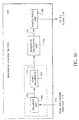
- the bandwidth control section 120 will be explained in further detail with reference to Figure 10 .
- the bandwidth control section 120 estimates the variance of the quantized phase error signal 126 and converts this into a dynamic bandwidth.
- the bandwidth control section 120 comprises four processing units: a squaring unit 160, a (leaky) integrator unit 162 , a bandwidth calculation unit 164 and a sample/hold unit 168 .
- the squaring unit 160 squares the quantized phase error signal 126 .
- the integrator 162 which is a first order low-pass filter, then integrates and smooths the squared signal 170.
- the squaring unit 160 and the integrator 172 act together to estimate the standard deviation (squared), or variance, 172 of the quantized phase error signal 126. This value 172 is then input into the bandwidth calculation unit 164.
- the bandwidth calculation unit 164 determines the desired bandwidth of the PLL filter 116 based upon the input value 172. The operation of the bandwidth calculation unit 164 will be explained in detail with reference to Figure 11. As shown, the bandwidth calculation unit 164 utilizes a select transfer function 180 to correlate the input signal 172 to a desired output bandwidth 174 .
- the transfer function is defined by four parameters: 1)BW HI - the widest bandwidth value; 2)BW LO - the narrowest bandwidth; 3) ⁇ HI - the highest value of the variance of the quantized phase error; and 4) ⁇ LO - the lowest value of the variance of the quantized phase error.
- BW HI is selected to produce the shortest initial lock-on time; typically 1000 Hz. The wider the bandwidth, the faster the initial lock-on period.
- BW LO is selected to provide the required PLL steady state error. Typically, 100 Hz provides 5 degree steady state error, which is acceptable for the present invention.
- ⁇ HI and ⁇ LO depend upon the input signal-to-noise ratio and the particular architecture and application.
- An initial estimate for ⁇ LO typically is obtained by operating the PLL 10 in an "ideal" mode (the PLL produces a perfect correction for each sample).
- An initial estimate for ⁇ HI is typically obtained by operating the PLL in the "worst case” mode (the PLL produces a random correction for each sample).
- the transfer function 180 comprises a linear portion 182 which correlates the input value 172 with the desired output bandwidth 174. It is preferable to limit the linear portion 182 of the transfer function 180 to a range of phase error input values 172 and bandwidth output values 174 in order to simplify the operation of the transfer function unit 164 .
- the transfer function 180 will provide a desired bandwidth output 174 of B .
- the bandwidth calculation unit 164 may be implemented by a microprocessor which would dynamically calculate the bandwidth. Additionally, the microprocessor may be dynamically updated with different transfer functions depending upon the conditions of the system and the RF channel.
- the bandwidth calculation unit 164 outputs the new bandwidth of the PLL filter 116 .
- the sampled bandwidth 130 from the sample/hold unit 168 is input to the PLL filter 116.
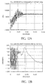
- Figure 12A shows the carrier offset frequency estimate (in Hertz) provided by the output of the lag filter 144 as a function of time in seconds.
- the average of the frequency estimate quickly reaches the true value of 7000Hz, but since the bandwidth is wide, the estimate is still noisy. As the bandwidth begins to narrow, the frequency estimate becomes less noisy. At 0.02 seconds, the bandwidth has narrowed significantly, and there is very little noise in the frequency estimate.
- Figure 12B shows the phase correction (in degrees) provided by the output of the lead filter 142 as a function of time (in seconds). This correction varies widely until initial lock-on of the PLL 10 at 0.01 seconds. Since the bandwidth is still wide at this point, the correction varies. As the bandwidth is narrowed, the variation in the correction is reduced. At 0.02 seconds, the bandwidth has narrowed significantly and the variation is minimized.
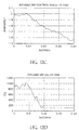
- Figure 12C shows the bandwidth control signal (in Radians 2 ) as a function of time (in seconds), which is a measure of the variance of the phase error.
- the variance begins to decrease which, in turn, causes the dynamic bandwidth to narrow (see Figure 12D ).
- the variance continues to decrease as the PLL 10 improves its ability to estimate phase correction.
- Figure 12D shows the dynamic bandwidth (in Hertz) as a function of time (in seconds).
- the bandwidth is near its maximum of 1000Hz up until initial lock-on of the PLL 10 at around 0.01 seconds. With lock-on, phase error is reduced, causing the bandwidth to begin narrowing. The bandwidth approaches it minimum of 100Hz as the phase error continues to be reduced.
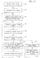
- the process for determining the amount of phase error, determining an appropriate PLL 10 bandwidth, adjusting the PLL 10 bandwidth and controlling the VCO 118 to provide an updated correction signal 50 is summarized in Figure 13 .
- the pilot signal 17 After the pilot signal 17 has been received (step 200 ) by the pilot rake receiver 40 , the pilot signal 17 is despread ( step 202 ) and corrected for channel distortion due to multipath reflections ( step 204 ).
- a complex error signal is produced ( step 206 ) and the error signal is normalized ( step 208 ) prior to quantizing the phase of the error signal ( step 210 ).
- the bandwidth control section 120 estimates the variance of the phase error ( step 214 ) and determines the desired PLL bandwidth to produce a correction signal ( step 216 ).
- the PLL filter 116 provides an estimate of the offset of the RF carrier signal and the phase error due to the carrier signal offset (step 212 ) and provides a correction signal ( step 218 ) to the pilot rake receiver 40 and the data receiver 42 . In this manner, the bandwidth of the PLL filter 116 is continuously adjusted and refined as the magnitude of the error signal 126 output from the arctangent analyzer 114 decreases.
Landscapes
- Engineering & Computer Science (AREA)
- Computer Networks & Wireless Communication (AREA)
- Signal Processing (AREA)
- Stabilization Of Oscillater, Synchronisation, Frequency Synthesizers (AREA)
- Digital Transmission Methods That Use Modulated Carrier Waves (AREA)
- Arc Welding Control (AREA)
- Networks Using Active Elements (AREA)
- Radar Systems Or Details Thereof (AREA)
- Superheterodyne Receivers (AREA)
Priority Applications (1)
| Application Number | Priority Date | Filing Date | Title |
|---|---|---|---|
| EP05000413A EP1538799A3 (en) | 1997-03-12 | 1998-03-11 | Phase-locked loop with continuously adjustable bandwidth |
Applications Claiming Priority (5)
| Application Number | Priority Date | Filing Date | Title |
|---|---|---|---|
| US3791497P | 1997-03-12 | 1997-03-12 | |
| US37914P | 1997-03-12 | ||
| US871109 | 1997-06-09 | ||
| US08/871,109 US6055231A (en) | 1997-03-12 | 1997-06-09 | Continuously adjusted-bandwidth discrete-time phase-locked loop |
| PCT/US1998/004691 WO1998040991A1 (en) | 1997-03-12 | 1998-03-11 | Phase-locked loop with continuously adjustable bandwith |
Related Child Applications (1)
| Application Number | Title | Priority Date | Filing Date |
|---|---|---|---|
| EP05000413A Division EP1538799A3 (en) | 1997-03-12 | 1998-03-11 | Phase-locked loop with continuously adjustable bandwidth |
Publications (2)
| Publication Number | Publication Date |
|---|---|
| EP0966819A1 EP0966819A1 (en) | 1999-12-29 |
| EP0966819B1 true EP0966819B1 (en) | 2005-01-12 |
Family
ID=26714619
Family Applications (1)
| Application Number | Title | Priority Date | Filing Date |
|---|---|---|---|
| EP98910290A Expired - Lifetime EP0966819B1 (en) | 1997-03-12 | 1998-03-11 | Phase-locked loop with continuously adjustable bandwith |
Country Status (8)
| Country | Link |
|---|---|
| US (5) | US6055231A (enExample) |
| EP (1) | EP0966819B1 (enExample) |
| JP (1) | JP3761587B2 (enExample) |
| AT (1) | ATE287171T1 (enExample) |
| DE (2) | DE69828589T2 (enExample) |
| DK (1) | DK0966819T3 (enExample) |
| ES (1) | ES2144985T3 (enExample) |
| WO (1) | WO1998040991A1 (enExample) |
Families Citing this family (40)
| Publication number | Priority date | Publication date | Assignee | Title |
|---|---|---|---|---|
| US6055231A (en) * | 1997-03-12 | 2000-04-25 | Interdigital Technology Corporation | Continuously adjusted-bandwidth discrete-time phase-locked loop |
| US6259687B1 (en) * | 1997-10-31 | 2001-07-10 | Interdigital Technology Corporation | Communication station with multiple antennas |
| US6208632B1 (en) * | 1998-01-29 | 2001-03-27 | Sharp Laboratories Of America | System and method for CDMA channel estimation |
| US6366607B1 (en) | 1998-05-14 | 2002-04-02 | Interdigital Technology Corporation | Processing for improved performance and reduced pilot |
| US6363102B1 (en) * | 1999-04-23 | 2002-03-26 | Qualcomm Incorporated | Method and apparatus for frequency offset correction |
| EP1530301B1 (en) | 2000-03-28 | 2010-04-21 | Interdigital Technology Corporation | Cdma system which uses pre-rotation before transmission |
| AU7397501A (en) * | 2000-05-05 | 2001-11-20 | Telefonaktiebolaget Lm Ericsson (Publ) | Method and apparatus to estimate frequency offset in a receiver |
| US6728301B1 (en) | 2000-07-07 | 2004-04-27 | Texas Instruments Incorporated | System and method for automatic frequency control in spread spectrum communications |
| US6683920B1 (en) | 2000-09-22 | 2004-01-27 | Applied Micro Circuits Corporation | Dual-loop system and method for frequency acquisition and tracking |
| JP2002280935A (ja) * | 2001-03-19 | 2002-09-27 | Sumitomo Electric Ind Ltd | 電力線搬送におけるマルチキャリア通信装置及び通信方法 |
| FR2824431A1 (fr) * | 2001-05-03 | 2002-11-08 | Mitsubishi Electric Inf Tech | Methode et dispositif de reception de signal |
| US7088955B2 (en) | 2001-07-16 | 2006-08-08 | Qualcomm Inc. | Method and apparatus for acquiring and tracking pilots in a CDMA communication system |
| US6904286B1 (en) * | 2001-07-18 | 2005-06-07 | Cisco Technology, Inc. | Method and system of integrated rate control for a traffic flow across wireline and wireless networks |
| US7430191B2 (en) * | 2001-09-10 | 2008-09-30 | Qualcomm Incorporated | Method and apparatus for performing frequency tracking based on diversity transmitted pilots in a CDMA communication system |
| US7539212B2 (en) * | 2001-11-26 | 2009-05-26 | Sami Kekki | Method and apparatus for MAC layer inverse multiplexing in a third generation radio access network |
| US7161996B1 (en) * | 2002-02-05 | 2007-01-09 | Airgo Networks, Inc. | Multi-antenna wireless receiver chains with vector decoding |
| JP3642053B2 (ja) * | 2002-02-25 | 2005-04-27 | 日本電気株式会社 | シンボルデータ変換回路 |
| US6760362B2 (en) * | 2002-03-15 | 2004-07-06 | Qualcomm Incorporated | Dynamic pilot filter bandwidth estimation |
| US7209532B2 (en) * | 2002-03-28 | 2007-04-24 | Harris Corporation | Phase lock loop and method for coded waveforms |
| US8306176B2 (en) * | 2002-06-19 | 2012-11-06 | Texas Instruments Incorporated | Fine-grained gear-shifting of a digital phase-locked loop (PLL) |
| US7760616B2 (en) * | 2002-07-31 | 2010-07-20 | Thomson Licensing | Extracting the phase of an OFDM signal sample |
| WO2004014005A1 (en) * | 2002-07-31 | 2004-02-12 | Thomson Licensing S.A. | Extracting the phase of an ofdm signal sample |
| EP1394974A3 (en) * | 2002-08-30 | 2005-08-03 | Zarlink Semiconductor Limited | Adaptive clock recovery in packet networks |
| US7916803B2 (en) | 2003-04-10 | 2011-03-29 | Qualcomm Incorporated | Modified preamble structure for IEEE 802.11a extensions to allow for coexistence and interoperability between 802.11a devices and higher data rate, MIMO or otherwise extended devices |
| US8743837B2 (en) * | 2003-04-10 | 2014-06-03 | Qualcomm Incorporated | Modified preamble structure for IEEE 802.11A extensions to allow for coexistence and interoperability between 802.11A devices and higher data rate, MIMO or otherwise extended devices |
| EP1751890B1 (en) * | 2004-05-27 | 2017-03-01 | QUALCOMM Incorporated | Modified preamble structure for ieee 802.11a extensions to allow for coexistence and interoperability between 802.11a devices and higher data rate, mimo or otherwise extended devices |
| US7646836B1 (en) * | 2005-03-01 | 2010-01-12 | Network Equipment Technologies, Inc. | Dynamic clock rate matching across an asynchronous network |
| US20060285618A1 (en) * | 2005-06-21 | 2006-12-21 | Ehud Shoor | Adaptive phase recovery |
| US7369002B2 (en) * | 2005-07-28 | 2008-05-06 | Zarlink Semiconductor, Inc. | Phase locked loop fast lock method |
| JP4699843B2 (ja) * | 2005-09-15 | 2011-06-15 | 富士通株式会社 | 移動通信システム、並びに移動通信システムにおいて使用される基地局装置および移動局装置 |
| US20070168085A1 (en) * | 2005-11-18 | 2007-07-19 | Guilford John H | Systems and method for adaptively adjusting a control loop |
| US7391271B2 (en) * | 2006-06-22 | 2008-06-24 | International Business Machines Corporation | Adjustment of PLL bandwidth for jitter control using feedback circuitry |
| US7751514B2 (en) * | 2007-05-23 | 2010-07-06 | Mediatek Inc. | System and method of detecting burst noise and minimizing the effect of burst noise |
| KR100929776B1 (ko) * | 2007-11-26 | 2009-12-03 | 한국전자통신연구원 | 리커시브 복조 장치 및 방법 |
| GB0800251D0 (en) | 2008-01-08 | 2008-02-13 | Zarlink Semiconductor Inc | Phase locked loop with adaptive filter for dco synchronization |
| US9097787B2 (en) * | 2009-11-12 | 2015-08-04 | Precyse Technologies, Inc. | Location method and system using colliding signals |
| KR101201116B1 (ko) | 2010-08-17 | 2012-11-13 | 성균관대학교산학협력단 | 동적 루프 대역을 갖는 위상고정루프 및 동적 루프 대역을 사용하여 기준신호에 동기하는 출력신호를 생성하는 방법 |
| EP2502393B1 (en) * | 2010-09-02 | 2015-07-01 | Huawei Technologies Co., Ltd. | Phase offset compensator |
| CN103312321A (zh) * | 2012-03-09 | 2013-09-18 | 联想(北京)有限公司 | 带宽调整方法、调节装置、锁相环电路和电子设备 |
| TWI605686B (zh) * | 2016-12-01 | 2017-11-11 | 晨星半導體股份有限公司 | 鎖相迴路單元的頻寬調整方法與相關的頻寬調整單元及相位回復模組 |
Family Cites Families (31)
| Publication number | Priority date | Publication date | Assignee | Title |
|---|---|---|---|---|
| US3983501A (en) * | 1975-09-29 | 1976-09-28 | The United States Of America As Represented By The Secretary Of The Navy | Hybrid tracking loop for detecting phase shift keyed signals |
| US4243941A (en) * | 1978-12-07 | 1981-01-06 | Motorola, Inc. | Digital signal receiver having a dual bandwidth tracking loop |
| US4354277A (en) * | 1979-11-23 | 1982-10-12 | Trw Inc. | Signal acquisition system |
| US4513429A (en) * | 1981-12-03 | 1985-04-23 | The United States Of America As Represented By The Secretary Of The Air Force | Sample data phase locked loop for adaptive doppler tracker |
| US4630283A (en) * | 1985-07-17 | 1986-12-16 | Rca Corporation | Fast acquisition burst mode spread spectrum communications system with pilot carrier |
| US5029180A (en) * | 1989-03-23 | 1991-07-02 | Echelon Systems Corporation | Transceiver providing selectable frequencies and spreading sequences |
| JPH082060B2 (ja) * | 1989-09-13 | 1996-01-10 | 日本電気株式会社 | 搬送波再生方式およびディジタル位相復調装置 |
| US5065107A (en) * | 1990-04-19 | 1991-11-12 | University Of Saskatchewan | Phase-locked loop bandwidth switching demodulator for suppressed carrier signals |
| FR2661752B1 (fr) * | 1990-05-07 | 1992-07-10 | Dassault Electronique | Recepteur d'un signal electromagnetique de frequence nominale connue susceptible d'etre affecte d'une variation inconnue, notamment par decalage doppler. |
| US5166952A (en) * | 1990-05-24 | 1992-11-24 | Cylink Corporation | Method and apparatus for the reception and demodulation of spread spectrum radio signals |
| US5390207A (en) * | 1990-11-28 | 1995-02-14 | Novatel Communications Ltd. | Pseudorandom noise ranging receiver which compensates for multipath distortion by dynamically adjusting the time delay spacing between early and late correlators |
| US5101416A (en) * | 1990-11-28 | 1992-03-31 | Novatel Comunications Ltd. | Multi-channel digital receiver for global positioning system |
| US5175729A (en) * | 1991-06-05 | 1992-12-29 | Motorola, Inc. | Radio with fast lock phase-locked loop |
| US5142246A (en) * | 1991-06-19 | 1992-08-25 | Telefonaktiebolaget L M Ericsson | Multi-loop controlled VCO |
| US5325405A (en) * | 1991-08-27 | 1994-06-28 | Motorola, Inc. | Burst mode receiver control |
| US5384550A (en) * | 1992-09-18 | 1995-01-24 | Rockwell International Corporation | Loop transient response estimator for improved acquisition performance |
| DE69406151T2 (de) * | 1993-01-13 | 1998-04-02 | Koninkl Philips Electronics Nv | Einrichtung zur Synchronisierung eines lokalen Trägers, in OFDM-Systemen |
| JPH06338829A (ja) * | 1993-05-28 | 1994-12-06 | American Teleph & Telegr Co <Att> | 通信システム内の反響除去方法と装置 |
| IL111469A0 (en) * | 1993-11-01 | 1994-12-29 | Omnipoint Corp | Despreading/demodulating direct sequence spread spectrum signals |
| DE69533022T2 (de) * | 1994-06-23 | 2005-04-07 | Ntt Docomo, Inc. | Cdma demodulationsschaltung und -verfahren |
| US5619524A (en) * | 1994-10-04 | 1997-04-08 | Motorola, Inc. | Method and apparatus for coherent communication reception in a spread-spectrum communication system |
| ZA9510509B (en) * | 1994-12-23 | 1996-05-30 | Qualcomm Inc | Dual-mode digital FM communication system |
| US5640431A (en) * | 1995-03-10 | 1997-06-17 | Motorola, Inc. | Method and apparatus for offset frequency estimation for a coherent receiver |
| US7020111B2 (en) * | 1996-06-27 | 2006-03-28 | Interdigital Technology Corporation | System for using rapid acquisition spreading codes for spread-spectrum communications |
| JP3013763B2 (ja) * | 1995-08-25 | 2000-02-28 | 日本電気株式会社 | キャリア同期ユニット |
| US5970093A (en) * | 1996-01-23 | 1999-10-19 | Tiernan Communications, Inc. | Fractionally-spaced adaptively-equalized self-recovering digital receiver for amplitude-Phase modulated signals |
| US5754583A (en) * | 1996-05-06 | 1998-05-19 | Motorola, Inc. | Communication device and method for determining finger lock status in a radio receiver |
| US6101176A (en) * | 1996-07-24 | 2000-08-08 | Nokia Mobile Phones | Method and apparatus for operating an indoor CDMA telecommunications system |
| US5900785A (en) * | 1996-11-13 | 1999-05-04 | Ericsson Inc. | System and method for offsetting load switching transients in a frequency synthesizer |
| US6115411A (en) * | 1996-12-31 | 2000-09-05 | Lucent Technologies, Inc. | System and method for spread spectrum code position modulation and wireless local area network employing the same |
| US6055231A (en) * | 1997-03-12 | 2000-04-25 | Interdigital Technology Corporation | Continuously adjusted-bandwidth discrete-time phase-locked loop |
-
1997
- 1997-06-09 US US08/871,109 patent/US6055231A/en not_active Expired - Lifetime
-
1998
- 1998-03-11 AT AT98910290T patent/ATE287171T1/de not_active IP Right Cessation
- 1998-03-11 JP JP53972498A patent/JP3761587B2/ja not_active Expired - Fee Related
- 1998-03-11 DE DE69828589T patent/DE69828589T2/de not_active Expired - Lifetime
- 1998-03-11 EP EP98910290A patent/EP0966819B1/en not_active Expired - Lifetime
- 1998-03-11 WO PCT/US1998/004691 patent/WO1998040991A1/en not_active Ceased
- 1998-03-11 ES ES98910290T patent/ES2144985T3/es not_active Expired - Lifetime
- 1998-03-11 DK DK98910290T patent/DK0966819T3/da active
- 1998-03-11 DE DE0966819T patent/DE966819T1/de active Pending
-
2000
- 2000-04-24 US US09/558,686 patent/US6608826B1/en not_active Expired - Fee Related
-
2003
- 2003-08-19 US US10/643,792 patent/US6940875B2/en not_active Expired - Fee Related
-
2005
- 2005-07-06 US US11/175,924 patent/US7145894B2/en not_active Expired - Fee Related
-
2006
- 2006-10-30 US US11/590,449 patent/US20070047511A1/en not_active Abandoned
Also Published As
| Publication number | Publication date |
|---|---|
| ES2144985T1 (es) | 2000-07-01 |
| US7145894B2 (en) | 2006-12-05 |
| US6608826B1 (en) | 2003-08-19 |
| US6055231A (en) | 2000-04-25 |
| HK1024365A1 (en) | 2000-10-05 |
| ATE287171T1 (de) | 2005-01-15 |
| DE69828589T2 (de) | 2006-03-16 |
| DE69828589D1 (de) | 2005-02-17 |
| DE966819T1 (de) | 2000-10-05 |
| US20040032842A1 (en) | 2004-02-19 |
| JP3761587B2 (ja) | 2006-03-29 |
| JP2001514831A (ja) | 2001-09-11 |
| US6940875B2 (en) | 2005-09-06 |
| EP0966819A1 (en) | 1999-12-29 |
| ES2144985T3 (es) | 2005-06-16 |
| US20070047511A1 (en) | 2007-03-01 |
| US20050243790A1 (en) | 2005-11-03 |
| DK0966819T3 (da) | 2005-05-23 |
| WO1998040991A1 (en) | 1998-09-17 |
Similar Documents
| Publication | Publication Date | Title |
|---|---|---|
| EP0966819B1 (en) | Phase-locked loop with continuously adjustable bandwith | |
| US6292477B1 (en) | Code division multiple access mobile communication system | |
| EP0675606B1 (en) | Receiver for spread spectrum communication | |
| US7145893B2 (en) | Communication station having an improved antenna system | |
| CA2189343C (en) | Method and apparatus for offset frequency estimation for a coherent receiver | |
| EP0774850B1 (en) | Digital signal detecting method and detector | |
| US6289004B1 (en) | Adaptive cancellation of fixed interferers | |
| CA2461336C (en) | Automatic frequency correction method and apparatus for time division duplex modes of 3g wireless communications | |
| US5844935A (en) | CDMA Receiver | |
| US6996156B1 (en) | CDMA receiver capable of estimation of frequency offset in high precision | |
| GB2342019A (en) | CDMA receiver with variable sampling rate | |
| JP4338310B2 (ja) | 通信システムのための高速同期 | |
| US5920555A (en) | Pilot assisted direct sequence spread spectrum synchronization apparatus | |
| AU750307B2 (en) | Automatic gain control circuit and control method therefor | |
| US7567624B1 (en) | System and method of communicating using combined signal parameter diversity | |
| EP1538799A2 (en) | Phase-locked loop with continuously adjustable bandwidth | |
| US6556619B2 (en) | Frequency adjusting circuit in code division multiple access communication system | |
| KR20020067601A (ko) | 스프레드 스펙트럼 통신 시스템에서의 옵셋 보정 | |
| HK1024365B (en) | Phase-locked loop with continuously adjustable bandwith | |
| HK1075561A (en) | Phase-locked loop with continuously adjustable bandwidth | |
| KR20040023440A (ko) | 이동통신시스템의 수신단에서의 주파수 오차 추정 및 결합기 | |
| EP1146658A1 (en) | Cdma radio receiver and cdma radio receiving method |
Legal Events
| Date | Code | Title | Description |
|---|---|---|---|
| PUAI | Public reference made under article 153(3) epc to a published international application that has entered the european phase |
Free format text: ORIGINAL CODE: 0009012 |
|
| 17P | Request for examination filed |
Effective date: 19991012 |
|
| AK | Designated contracting states |
Kind code of ref document: A1 Designated state(s): AT BE CH DE DK ES FI FR GB GR IE IT LI LU MC NL PT SE |
|
| EL | Fr: translation of claims filed | ||
| REG | Reference to a national code |
Ref country code: ES Ref legal event code: BA2A Ref document number: 2144985 Country of ref document: ES Kind code of ref document: T1 |
|
| DET | De: translation of patent claims | ||
| 17Q | First examination report despatched |
Effective date: 20031001 |
|
| GRAP | Despatch of communication of intention to grant a patent |
Free format text: ORIGINAL CODE: EPIDOSNIGR1 |
|
| RIN1 | Information on inventor provided before grant (corrected) |
Inventor name: CERDA, RAMON Inventor name: YANG, RUI Inventor name: MESECHER, DAVID, K. |
|
| GRAS | Grant fee paid |
Free format text: ORIGINAL CODE: EPIDOSNIGR3 |
|
| GRAA | (expected) grant |
Free format text: ORIGINAL CODE: 0009210 |
|
| AK | Designated contracting states |
Kind code of ref document: B1 Designated state(s): AT BE CH DE DK ES FI FR GB GR IE IT LI LU MC NL PT SE |
|
| PG25 | Lapsed in a contracting state [announced via postgrant information from national office to epo] |
Ref country code: NL Free format text: LAPSE BECAUSE OF FAILURE TO SUBMIT A TRANSLATION OF THE DESCRIPTION OR TO PAY THE FEE WITHIN THE PRESCRIBED TIME-LIMIT Effective date: 20050112 Ref country code: BE Free format text: LAPSE BECAUSE OF FAILURE TO SUBMIT A TRANSLATION OF THE DESCRIPTION OR TO PAY THE FEE WITHIN THE PRESCRIBED TIME-LIMIT Effective date: 20050112 Ref country code: AT Free format text: LAPSE BECAUSE OF FAILURE TO SUBMIT A TRANSLATION OF THE DESCRIPTION OR TO PAY THE FEE WITHIN THE PRESCRIBED TIME-LIMIT Effective date: 20050112 |
|
| REG | Reference to a national code |
Ref country code: GB Ref legal event code: FG4D |
|
| REG | Reference to a national code |
Ref country code: CH Ref legal event code: EP |
|
| REG | Reference to a national code |
Ref country code: CH Ref legal event code: NV Representative=s name: SCHMAUDER & PARTNER AG PATENTANWALTSBUERO |
|
| REF | Corresponds to: |
Ref document number: 69828589 Country of ref document: DE Date of ref document: 20050217 Kind code of ref document: P |
|
| REG | Reference to a national code |
Ref country code: IE Ref legal event code: FG4D |
|
| PG25 | Lapsed in a contracting state [announced via postgrant information from national office to epo] |
Ref country code: LU Free format text: LAPSE BECAUSE OF NON-PAYMENT OF DUE FEES Effective date: 20050311 Ref country code: IE Free format text: LAPSE BECAUSE OF NON-PAYMENT OF DUE FEES Effective date: 20050311 |
|
| PGFP | Annual fee paid to national office [announced via postgrant information from national office to epo] |
Ref country code: CH Payment date: 20050316 Year of fee payment: 8 |
|
| PG25 | Lapsed in a contracting state [announced via postgrant information from national office to epo] |
Ref country code: MC Free format text: LAPSE BECAUSE OF NON-PAYMENT OF DUE FEES Effective date: 20050331 |
|
| REG | Reference to a national code |
Ref country code: SE Ref legal event code: TRGR |
|
| REG | Reference to a national code |
Ref country code: DK Ref legal event code: T3 |
|
| REG | Reference to a national code |
Ref country code: ES Ref legal event code: FG2A Ref document number: 2144985 Country of ref document: ES Kind code of ref document: T3 |
|
| NLV1 | Nl: lapsed or annulled due to failure to fulfill the requirements of art. 29p and 29m of the patents act | ||
| REG | Reference to a national code |
Ref country code: HK Ref legal event code: GR Ref document number: 1024365 Country of ref document: HK |
|
| PLBE | No opposition filed within time limit |
Free format text: ORIGINAL CODE: 0009261 |
|
| STAA | Information on the status of an ep patent application or granted ep patent |
Free format text: STATUS: NO OPPOSITION FILED WITHIN TIME LIMIT |
|
| REG | Reference to a national code |
Ref country code: IE Ref legal event code: MM4A |
|
| ET | Fr: translation filed | ||
| 26N | No opposition filed |
Effective date: 20051013 |
|
| PG25 | Lapsed in a contracting state [announced via postgrant information from national office to epo] |
Ref country code: LI Free format text: LAPSE BECAUSE OF NON-PAYMENT OF DUE FEES Effective date: 20060331 Ref country code: CH Free format text: LAPSE BECAUSE OF NON-PAYMENT OF DUE FEES Effective date: 20060331 |
|
| REG | Reference to a national code |
Ref country code: CH Ref legal event code: PL |
|
| PG25 | Lapsed in a contracting state [announced via postgrant information from national office to epo] |
Ref country code: PT Free format text: LAPSE BECAUSE OF NON-PAYMENT OF DUE FEES Effective date: 20050612 |
|
| PG25 | Lapsed in a contracting state [announced via postgrant information from national office to epo] |
Ref country code: GR Free format text: LAPSE BECAUSE OF NON-PAYMENT OF DUE FEES Effective date: 20050112 |
|
| PGFP | Annual fee paid to national office [announced via postgrant information from national office to epo] |
Ref country code: SE Payment date: 20140311 Year of fee payment: 17 Ref country code: DK Payment date: 20140311 Year of fee payment: 17 Ref country code: FI Payment date: 20140311 Year of fee payment: 17 |
|
| PGFP | Annual fee paid to national office [announced via postgrant information from national office to epo] |
Ref country code: FR Payment date: 20140311 Year of fee payment: 17 Ref country code: ES Payment date: 20140211 Year of fee payment: 17 Ref country code: IT Payment date: 20140307 Year of fee payment: 17 |
|
| PGFP | Annual fee paid to national office [announced via postgrant information from national office to epo] |
Ref country code: GB Payment date: 20140305 Year of fee payment: 17 |
|
| PGFP | Annual fee paid to national office [announced via postgrant information from national office to epo] |
Ref country code: DE Payment date: 20140417 Year of fee payment: 17 |
|
| REG | Reference to a national code |
Ref country code: DE Ref legal event code: R119 Ref document number: 69828589 Country of ref document: DE |
|
| REG | Reference to a national code |
Ref country code: DK Ref legal event code: EBP Effective date: 20150331 |
|
| PG25 | Lapsed in a contracting state [announced via postgrant information from national office to epo] |
Ref country code: FI Free format text: LAPSE BECAUSE OF NON-PAYMENT OF DUE FEES Effective date: 20150311 |
|
| GBPC | Gb: european patent ceased through non-payment of renewal fee |
Effective date: 20150311 |
|
| PG25 | Lapsed in a contracting state [announced via postgrant information from national office to epo] |
Ref country code: SE Free format text: LAPSE BECAUSE OF NON-PAYMENT OF DUE FEES Effective date: 20150312 |
|
| REG | Reference to a national code |
Ref country code: SE Ref legal event code: EUG |
|
| PG25 | Lapsed in a contracting state [announced via postgrant information from national office to epo] |
Ref country code: IT Free format text: LAPSE BECAUSE OF NON-PAYMENT OF DUE FEES Effective date: 20150311 |
|
| REG | Reference to a national code |
Ref country code: FR Ref legal event code: ST Effective date: 20151130 |
|
| PG25 | Lapsed in a contracting state [announced via postgrant information from national office to epo] |
Ref country code: GB Free format text: LAPSE BECAUSE OF NON-PAYMENT OF DUE FEES Effective date: 20150311 Ref country code: DE Free format text: LAPSE BECAUSE OF NON-PAYMENT OF DUE FEES Effective date: 20151001 |
|
| PG25 | Lapsed in a contracting state [announced via postgrant information from national office to epo] |
Ref country code: FR Free format text: LAPSE BECAUSE OF NON-PAYMENT OF DUE FEES Effective date: 20150331 |
|
| PG25 | Lapsed in a contracting state [announced via postgrant information from national office to epo] |
Ref country code: DK Free format text: LAPSE BECAUSE OF NON-PAYMENT OF DUE FEES Effective date: 20150331 |
|
| REG | Reference to a national code |
Ref country code: ES Ref legal event code: FD2A Effective date: 20160429 |
|
| PG25 | Lapsed in a contracting state [announced via postgrant information from national office to epo] |
Ref country code: ES Free format text: LAPSE BECAUSE OF NON-PAYMENT OF DUE FEES Effective date: 20150312 |