EP0966727B1 - Kompaktes sensorsystem zur optischen bewegungserkennung in echtzeit - Google Patents
Kompaktes sensorsystem zur optischen bewegungserkennung in echtzeit Download PDFInfo
- Publication number
- EP0966727B1 EP0966727B1 EP98907892A EP98907892A EP0966727B1 EP 0966727 B1 EP0966727 B1 EP 0966727B1 EP 98907892 A EP98907892 A EP 98907892A EP 98907892 A EP98907892 A EP 98907892A EP 0966727 B1 EP0966727 B1 EP 0966727B1
- Authority
- EP
- European Patent Office
- Prior art keywords
- image data
- sensor system
- optical flow
- image
- logic
- Prior art date
- Legal status (The legal status is an assumption and is not a legal conclusion. Google has not performed a legal analysis and makes no representation as to the accuracy of the status listed.)
- Expired - Lifetime
Links
Images


Classifications
-
- G—PHYSICS
- G06—COMPUTING OR CALCULATING; COUNTING
- G06T—IMAGE DATA PROCESSING OR GENERATION, IN GENERAL
- G06T7/00—Image analysis
- G06T7/20—Analysis of motion
- G06T7/269—Analysis of motion using gradient-based methods
-
- H—ELECTRICITY
- H04—ELECTRIC COMMUNICATION TECHNIQUE
- H04N—PICTORIAL COMMUNICATION, e.g. TELEVISION
- H04N25/00—Circuitry of solid-state image sensors [SSIS]; Control thereof
Definitions
- the invention relates to a compact sensor system for optical Motion detection through real-time calculation of the x and y components the optical flow from an image sequence according to a predetermined Algorithm with a two-dimensional photodiode matrix based image data unit with an adjustment area and a at least in sections sequential image data output and with one a user-specific, high-rate CMOS logic module Image data processing unit with a preprocessing and a Calculation logic and an external, optionally via two parallel ports accessible working memory and a control unit.
- the compact, high-rate sensor system known from this article lies to comply with the real-time condition a drastically in its complexity reduced and thus approximated correlation method (1D correlation) as Algorithm, in which not the correlated optical flow for small complete image sections, but its correlated components in the x and y directions to be calculated separately.
- the technical problem area with which the invention is concerned relates to the further development of a como-active sensor system with a high calculation speed of the type described at the outset in such a way that it can be inexpensively equipped and manufactured and combined with generally available means, and thereby a continuous calculation of the optical flow in real time also for very large and segmentable image areas with good image resolution, processing speed and accuracy.
- the compact sensor system should have a wide range of uses, in particular it should be capable of being designed in such a miniaturized form that application requirements can be met with extremely little space for the sensor.
- the solution according to the invention for this task field provides that in the image data processing unit the implementation of a continuous iterative calculation of the x and y components of the optical flow according to the gradient algorithm from Hom and Schunck is carried out exclusively by a digital hardware architecture of the user-specific CMOS logic module in the form of a consistent pipeline structure with a simple data feedback, into which the preprocessing logic with a first arithmetic arithmetic unit by connecting a first shift register and the calculation logic with three further arithmetic arithmetic units by connecting three further shift registers and with one pipeline stage having integrated block for calculating the optical flow, and that the external working memory is constructed from three identical memory elements, each one of the three further arithmetic units are arranged
- the new pipeline architecture is essential for the invention in the image data processing unit for a continuous calculation of the optical flow in real time.
- the optical flow can with the sensor according to the invention over large image areas, for example up to 512 x 512 motion vectors can be calculated. All applications in which different movements are segmented, need an optical Flow calculation for very large image areas.
- the Software relief for the user-oriented logic module (CMOS-ASIC) the hardware implementation increases the image processing capacity in Direction of the large image areas.
- the image processing speed can up to 1500 frames / second and is ultimately only of the Performance of the image data provider dependent.
- the straight forward Computing architecture can easily be implemented in digital hardware and in one Integrated circuit using a CMOS standard cell process be implemented. This is an established and manageable one Technology.
- the working memory consists of three identical ones Storage elements that are commercially available. Through that completely sequential reading and processing of image data is optimal Connection to commercially available image data providers. The format and that completely sequential writing of the speed vectors in the optical Flow allow easy connection to external commercial Segmentation and image processing systems (frame grabber cards or similar).
- the two-dimensional Photodiode matrix from a standardized image data generator with a completely sequential data output is formed. It can be for example around a CCD chip with associated driver circuits or are a CMOS photodiode matrix. Both imagers are commercially available available and therefore inexpensive. Expensive special designs for the Image data providers, which may also carry out preprocessing steps are not required. Additional circuits are necessary for Adaptation of the image data provider used to the Image data processing unit. According to a further continuation of the The idea of the invention is therefore favorable if the range of adaptation is one external, freely programmable logic module is formed.
- an FPGA field programmable gate array
- the functionality of the FPGA is not considered Part of the image data processing unit implemented, a certain one is achieved Design flexibility. You can also use it, for example additional synchronization signals for a digital sensor interface, the Image data generator and image data processing unit more locally independent from each other.
- Pipeline structures are well known in image processing because they are particularly suitable for continuous calculations. They excel in generally characterized by the fact that during a multi-stage data processing process the data is available in all stages of processing. With the clock signal, a date is first read into the first stage and processed and then passed on to the next processing stage, while a new date is already being imported into the first stage. On this way, the entire pipeline is filled cycle by cycle. The number of Bars that a date needs to run through the entire pipeline is called Referred to as latency. If you read a new date with every bar and a Write the result, you have a pipeline with maximum data throughput.
- the preprocessing and calculation logic consistently upstream of shift registers in the pipeline structure inserted.
- the shift registers each have two memory elements there is free access and a common address counter.
- the Most standard cell processes offer the option of using RAM memory cells in a particularly compact way.
- Tietze and Schenk show how RAM's can be operated as shift registers if a counter has the addresses counted cyclically. Be multiple values for a calculation at the same time needed, for example two RAM's with a common one Address counter can be used. For further information on this see special description part.
- control unit can be advantageous be implemented in the user-specific logic module. It is through it can be produced together with this in a simple standard cell process.
- the gradient equation (1) describes an undetermined system of equations with the 2 unknowns u and v . Only the velocity components orthogonal to the iso-intensity curves can be determined. An additional condition is therefore necessary.
- the flow components u (x, y) and v (x, y) can be determined by minimizing the following equation: ⁇ 2 ⁇ ( u x 2 + u y 2 + v x 2 + v y 2 ) dxdy + ⁇ ( I. x ⁇ U + I. v ⁇ V + I. t ) 2 dxdt
- the first term of equation (2) represents the smoothness condition.
- the second term is the gradient equation.
- ⁇ is called the smoothness parameter.
- the weighting of both terms is determined by choosing a suitable value for ⁇ .
- the partial local-time derivatives I x , I y and I t can be approximated as the difference in the intensities between two neighboring points in place and time.
- the indices n and n + 1 indicate the iteration steps.
- the components u and v are approximated by the mean of the adjacent flow components, as calculated in the previous iteration step.
- the iteration can be reduced to a loop (iteration value 1).
- simple data feedback a certain number of images (approximately 10 to 20) must be processed at the start of the optical flow calculation (processing time less than 1 second) before a correct calculation is available. This phase is called the initialization phase. A new correct optical flow field is then calculated with each image, ie the surroundings can be observed continuously.
- FIG. 1 schematically shows a sensor system 1 which is made up of several functional units.
- a functional image data generator unit 2 consists of an image data generator 3 and an adaptation area 4.
- the adaptation region 4 lies outside the image data generator 3 and is formed here by an external, freely programmable logic module 5 in the form of an FPGA as an independent further functional unit.
- This generates the addresses for the image data generator 3 and additionally generates synchronization signals in the horizontal ( HSYNC ) and vertical image direction ( VSYNC ). It also outputs the clock signal ( pixel clock ). All of these signals can be required in a further processing unit (not shown further) for the components of the optical flow.
- the image data generator 3 supplies the input values for an image data processing unit 6 as a further functional unit.
- these input values consist of a serial stream of the gray values of the pixels and are 8-bit (1 byte) wide, which corresponds to the gray values from 0 to 255.
- the data stream is driven by the clock signal and controlled by a synchronization signal (FrameSync), which marks the beginning of a new picture.
- the image data processing unit 6 reads this data and calculates the optical flow from it.
- the result is a two-dimensional field of motion vectors that can be temporarily stored in a result memory or processed directly by external image processing devices.
- the vectors represent the x and y components of the velocity field, which are also represented as an 8-bit value, and each correspond to a pixel.
- the unit of speed is distance / time.
- the unit of time results from the frame rate.
- the optical flow is measured in pixels / image (pixel / frame) and coded in the form of 8-bit values in the invention.
- the value 127 corresponds to 0 pixel / frame.
- Speeds between -4 and +4 pixel / frame can be displayed. The smallest speed that can be represented corresponds to approximately 0.016 pixel / frame.
- the image data processing unit 6 has a user-specific CMOS logic module 7 (ASIC - Application Specific Integrated Circuit) and an external working memory 8 .
- CMOS logic module 7 ASIC - Application Specific Integrated Circuit
- This is formed by three identical memory elements 9, 10, 11 in the form of memory elements with static, ie continuous power supply (dual-ported SRAM, commercially available) that can be optionally accessed via two parallel ports, each of which can store data corresponding to the size of an image.
- the addresses for the memory elements 9, 10, 11, which are operated here as shift registers with a storage capacity for a complete image, and all control signals that arise from the clock signal and the image start signal are generated by a functional control unit 12 . which is also implemented in logic module 7 .
- the image data processing unit 6 is shown in more detail in a block diagram. Due to the continuous flow of image data, a processing pipeline forms the ideal hardware architecture for this.
- the data path is subdivided into several functional blocks: preprocessing logic 13, block for derivation formation 17, block for calculating the optical flow 21 and block for local averaging of the optical flow components 22, which represents the iterative data feedback path.
- the blocks 17, 21 and 22 are combined in the calculation logic 14 .
- the pipeline length (latency) in the selected exemplary embodiment for the entire image data processing unit 6 relates to four image lines and 13 pixels.
- the image data read sequentially pixel by pixel into the image data processing unit 6 are first smoothed in the preprocessing logic 13 in order to increase the signal-to-noise ratio.
- the preprocessing logic 13 has a memory unit in the form of a first shift register 15 and a first arithmetic unit 16 for weighted averaging for smoothing.
- Such an implementation is known for example from "Synthesis of a Convolver, a Generic Module for the Codesign of Reconfigurable Pipelined Accelerators" (B. Bosi et al., Workshop on Filed-Programmable Devices, Montreal, May 1995, pp.44.48).
- the first arithmetic unit 16 calculates the gray value for a smoothed image for a pixel from the value for the central pixel and the values of the neighboring pixels. For this purpose, the value of the middle pixel is multiplied by four, added to the values of the neighboring pixels and the result is then normalized by dividing by eight. Multiplication and division are implemented by shifting operations.
- the smoothing operation is inserted into the pipeline structure by connecting the first shift register 15 with a minimum storage capacity for two image lines, since this is not very suitable for a pipeline structure due to the required parallel access to a plurality of image data values.
- the parallel reading in of the data of two image lines with a shift register is explained in more detail in FIG. 3 and the structure of a shift register integrated in a CMOS standard cell process in FIG. 4.
- the block for the derivation 17 for calculating the local (I x , I y ) and the temporal (I t ) derivations is constructed similarly to the preprocessing logic 13 . It consists of a shift register 18 and a further arithmetic unit 19. I x is the difference between the right and left intensity values with respect to the center pixel, I y is the difference between the upper and lower values. I t is the difference to the value of the corresponding pixel in the previous image. All derivatives are calculated in parallel. In order to form the time difference, the image data of a complete smoothed image must be buffered. Therefore, a first external DualPorted SRAM 20 is used. This makes it possible to carry out write and read access during a pixel clock.
- the memory is operated as a shift register.
- the size of the memory corresponds to that of the entire image.
- the control unit 12 (see FIG. 1), which is not shown further in FIG. 2, cyclically generates the addresses and the control signals for the memory 20.
- the block for calculating the optical flow 21 is described in more detail in FIG.
- the block for local averaging of the optical flow components 22 is implemented in a data feedback. It comprises two parallel paths for the two flow components u and v in, in which a third and fourth shift registers 23-24, a third and fourth arithmetic unit 25,26 and a second and third external dual-ported SRAM 27,28 having the storage capacity for a complete picture are arranged.
- the x and y components of the optical flow are processed in parallel.
- the averaging results, similar to the preprocessing logic 13, from the summation of the intensity values of the four pixels adjacent to a central pixel and the subsequent division by four. Since the values are only included in the calculation of the values of the next image n + 1 , the data are temporarily stored in the memories 27, 28 .
- the addresses and the control signals are in turn generated by the control unit 12 (see FIG. 1), which is not shown here.
- FIG. 3 shows schematically how reading two image lines into a shift register enables simultaneous access to the value of a central pixel and to the values of the neighboring pixels in the vicinity. This means that these values can be used in parallel for averaging and forming differences.
- FIG. 4 shows the implementation of a shift register in a standard CMOS cell process. Due to the large space requirement, the entire shift register cannot be constructed from standard cells. For this reason, two RAMs are implemented that can be generated in a particularly compact manner and whose addresses can be counted cyclically using a common counter. Two RAMs are required because parallel access to the central pixel and the right and left neighbors must be possible. The control signals for the RAMs have the correspondingly adapted, generally known temporal profile.
- the shift registers 15, 18, 23, 24 can be structurally combined with the associated arithmetic computing units 16, 19, 25, 26 to form a functional block of the logic module 7 (ASIC, see FIG. 1).
- the core of the calculation logic 14 is the block for calculating the optical flow 21, in which the components of the optical flow in the image n + 1 from those of the previous image n and the local and temporal derivatives of the image intensity in a simple iteration with that described above Algorithm can be calculated in parallel. However, the calculation cannot take place during a single pixel cycle. The correct ratio between the calculation speed and the chip size results from the appropriate choice of the number of pipeline stages required. If division operations are carried out as repeated subtraction and comparison operations, eight of a total of eleven pipeline steps are required to carry them out in the exemplary embodiment.
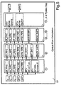
- FIG. 5 schematically shows the pipeline structure of the block for calculating the optical flow 21 .
- the new components u (n + 1), v (n + 1 ) are calculated according to equation (3) described above. This is implemented in block 21 .
- the sizes MY and NY for divisor and dividend are calculated in the equation.
- pipeline stage 2 these are then prepared for the division by shifting operations.
- pipeline stages 3..10 the division is carried out by repeated comparison and subtraction processes. Values that are not currently required for a calculation are read into the shift register (...- PIPE) and pushed through to the last pipeline stage 11 , in which the flow components are calculated.
- the output signal of the image data calculation unit can be directly via further processing commercially available DSP modules Image processing units are supplied. Two-Dimensional First order models can be applied to the measured optical flow become. Furthermore, the two-dimensional projection of the spatial motion suitable parameters of segmented moving objects and surface properties, such as the spatial orientation and the time until Clash to be won. More details on chip design method, Implementation and design data for a real execution case in an application of a navigable robot platform, this cannot Pre-published essay "A Real-Time Smart Sensor System for Visual Motion Estimation "by Th. Röwekamp et al.
- Smart Sensor System used for sensor systems that have a sensory element, for example an image data provider, and processing elements with each other connect.
Landscapes
- Engineering & Computer Science (AREA)
- Multimedia (AREA)
- Signal Processing (AREA)
- Computer Vision & Pattern Recognition (AREA)
- Physics & Mathematics (AREA)
- General Physics & Mathematics (AREA)
- Theoretical Computer Science (AREA)
- Image Processing (AREA)
Description

- Figur 1
- eine biockschematische Übersicht über die Systemarchitektur des erfindungsgemäßen Sensorsystems mit Erläuterungen zu einer realisierten Ausführungsform,
- Figur 2
- ein Blockdiagramm des Datenweges in der Bilddatenverarbeitungseinheit,
- Figur 3
- den schematischen Aufbau eines Schieberegister,
- Figur 4
- den Speicherzugriff in einem Schieberegister und
- Figur 5
- den blockschematischen Aufbau der Pipelinestruktur in der Berechnungslogik.
- 1
- Sensorsystem
- 2
- Bilddatengebereinheit
- 3
- Bilddatengeber
- 4
- Anpassungsbereich
- 5
- Logikbaustein
- 6
- Bilddatenverarbeitungseinheit
- 7
- anwenderspezifischer Logikbaustein
- 8
- externer Arbeitsspeicher
- 9
- erstes Speicherelement
- 10
- zweites Speicherelement
- 11
- drittes Speicherelement
- 12
- Kontrolleinheit
- 13
- Vorverarbeitungslogik
- 14
- Berechnungslogik
- 15
- erstes Schieberegister
- 16
- erste arithmetische Einheit
- 17
- Block zur Ableitungsbildung
- 18
- zweites Schieberegister
- 19
- zweite arithmetische Einheit
- 20
- erster externer DualPorted SRAM
- 21
- Block zur Berechnung des optischen Flusses
- 22
- Block zur lokalen Mittelwertbildung der optischen Flusskomponenten
- 23
- drittes Schieberegister
- 24
- viertes Schieberegister
- 25
- dritte arithmetische Einheit
- 26
- vierte arithmetische Einheit
- 27
- zweiter externer DualPorted SRAM
- 28
- dritter externer DualPorted SRAM
Claims (5)
- Kompaktes Sensorsystem zur optischen Bewegungserkennung durch Echtzeit-Berechnung der x- und y-Komponenten des optischen Flusses aus einer Bildfolge nach einem vorgegebenen Algorithmusdadurch gekennzeichnet, dassmit einer auf einer zweidimensionalen Photodiodenmatrix basierenden Bilddatengebereinheit mit einem Anpassungsbereich und einer zumindest abschnittsweise sequentiellen Bilddatenausgabe undmit einer auf einem anwenderspezifischen CMOS-Logikbaustein basierenden hochratigen Bilddatenverarbeitungseinheit mit einer Vorverarbeitungs- und einer Berechnungslogik sowie einem externen, wahlfrei über zwei Parallelports zugänglichen Arbeitsspeicher und einer Kontroileinheit,
in der Bilddatenverarbeitungseinheit (6) die Umsetzung einer kontinuierlichen iterativen Berechnung der x- und y-Komponenten des optischen Flusses nach dem Gradienten-Algorithmus von Horn und Schunck ausschließlich durch eine digitale Hardware-Architektur des anwenderspezifischen CMOS-Logikbausteins (7) in Form einer konsequenten Pipeline-Struktur mit einer einfachen Datenrückführung (22) realisiert ist, in die die Vorverarbeitungslogik (13) mit einer ersten arithmetischen Recheneinheit (16) durch das Vorschalten von einem ersten Schieberegister (15) und die Berechnungslogik (14) mit drei weiteren arithmetischen Recheneinheiten (19, 25, 26) durch das Vorschalten von drei weiteren Schieberegistern (18, 23, 24) und mit einem mehrere Pipelinestufen aufweisenden Block zur Berechnung des optischen Flusses (21) integriert sind, und dass der externe Arbeitsspeicher (8) aus drei identischen Speicherelementen (9,10,11; 20,27,28) aufgebaut ist, die jeweils einer der drei weiteren arithmetischen Einheiten (19, 25, 26) zugeordnet sind. - Kompaktes Sensorsystem nach Anspruch 1,
dadurch gekennzeichnet, dass
die zweidimensionale Photodiodenmatrix von einem standardisierten Bilddatengeber (3) mit einer vollständig sequentiellen Datenausgabe gebildet ist. - Kompaktes Sensorsystem nach Anspruch 1 oder 2,
dadurch gekennzeichnet, dass
der Anpassungsbereich (4) von einem externen, freiprogrammierbaren Logikbaustein (5) gebildet ist. - Kompaktes Sensorsystem nach einem der Ansprüche 1 bis 3,
dadurch gekennzeichnet, dass
die Schieberegister (15, 18, 23, 24) jeweils aus zwei Speicherelementen mit wahlfreiem Zugang und einem gemeinsamen Adressenzähler bestehen. - Kompaktes Sensorsystem nach einem der Ansprüche 1 bis 4,
dadurch gekennzeichnet, dass
die Kontrolleinheit (12) im anwenderspezifischen Logikbaustein (7) implementiert ist.
Applications Claiming Priority (3)
| Application Number | Priority Date | Filing Date | Title |
|---|---|---|---|
| DE19712017A DE19712017A1 (de) | 1997-03-15 | 1997-03-15 | Kompaktes Sensorsystem zur optischen Bewegungserkennung in Echtzeit |
| DE19712017 | 1997-03-15 | ||
| PCT/DE1998/000413 WO1998041950A1 (de) | 1997-03-15 | 1998-02-11 | Kompaktes sensorsystem zur optischen bewegungserkennung in echtzeit |
Publications (2)
| Publication Number | Publication Date |
|---|---|
| EP0966727A1 EP0966727A1 (de) | 1999-12-29 |
| EP0966727B1 true EP0966727B1 (de) | 2001-08-16 |
Family
ID=7824254
Family Applications (1)
| Application Number | Title | Priority Date | Filing Date |
|---|---|---|---|
| EP98907892A Expired - Lifetime EP0966727B1 (de) | 1997-03-15 | 1998-02-11 | Kompaktes sensorsystem zur optischen bewegungserkennung in echtzeit |
Country Status (3)
| Country | Link |
|---|---|
| EP (1) | EP0966727B1 (de) |
| DE (2) | DE19712017A1 (de) |
| WO (1) | WO1998041950A1 (de) |
Families Citing this family (6)
| Publication number | Priority date | Publication date | Assignee | Title |
|---|---|---|---|---|
| AT414056B (de) * | 2001-03-13 | 2006-08-15 | Siemens Ag Oesterreich | Verfahren zur überwachung einer lifttrasse und ihrer umgebung |
| ES2233202B1 (es) * | 2003-11-24 | 2006-10-16 | Universidad De Granada | Dispositivo para la estimacion de flujo optico en imagenes mediante fpgas. |
| US8170109B2 (en) | 2006-03-23 | 2012-05-01 | Nds Limited | System for analysis of motion |
| DE102007049706A1 (de) * | 2007-10-17 | 2009-04-23 | Robert Bosch Gmbh | Verfahren zur Schätzung der Relativbewegung von Video-Objekten und Fahrerassistenzsystem für Kraftfahrzeuge |
| DE102008052930B4 (de) * | 2008-10-23 | 2011-04-07 | Leuze Electronic Gmbh & Co Kg | Bildverarbeitender Sensor |
| EP3743690B1 (de) | 2019-03-26 | 2024-09-04 | Salunda Limited | Sensoreinheit für befestigungsanordnung |
Family Cites Families (1)
| Publication number | Priority date | Publication date | Assignee | Title |
|---|---|---|---|---|
| JP2789967B2 (ja) * | 1992-11-02 | 1998-08-27 | 松下電器産業株式会社 | 動きベクトル検出装置 |
-
1997
- 1997-03-15 DE DE19712017A patent/DE19712017A1/de not_active Withdrawn
-
1998
- 1998-02-11 WO PCT/DE1998/000413 patent/WO1998041950A1/de not_active Ceased
- 1998-02-11 DE DE59801214T patent/DE59801214D1/de not_active Expired - Fee Related
- 1998-02-11 EP EP98907892A patent/EP0966727B1/de not_active Expired - Lifetime
Also Published As
| Publication number | Publication date |
|---|---|
| DE59801214D1 (de) | 2001-09-20 |
| EP0966727A1 (de) | 1999-12-29 |
| WO1998041950A1 (de) | 1998-09-24 |
| DE19712017A1 (de) | 1998-09-17 |
Similar Documents
| Publication | Publication Date | Title |
|---|---|---|
| DE69728247T2 (de) | Pyramidenförmiger pipeline-prozessor für ein bildverarbeitungssystem | |
| DE69430153T2 (de) | Verfahren und Vorrichtung zur dreidimensionalen Bilderzeugung von Objekten | |
| DE69231812T2 (de) | Verfahren zur bestimmung von fuehlerbewegung und szenenstruktur und bildverarbeitungssystem dafuer | |
| DE69434657T2 (de) | System und Verfahren zur elektronischen Bildstabilisierung | |
| DE102008052930B4 (de) | Bildverarbeitender Sensor | |
| DE102008034979B4 (de) | Verfahren und Einrichtung zur Erzeugung von fehlerreduzierten hochauflösenden und kontrastverbesserten Bildern | |
| DE69520974T2 (de) | Eine integrierte Halbleiterschaltung | |
| DE69217550T2 (de) | Echt-zeit-erkennung von zeigerinformation durch video | |
| DE69127809T2 (de) | Verfahren um zwei bewegungen in hintereinanderfolgenden teilbildern mit drei teilbildern dynamisch zu analysieren | |
| EP2406769B1 (de) | Verfahren und vorrichtung zur reduktion des speicherbedarfs bei der bestimmung von disparitätswerten für mindestens zwei stereoskopisch aufgenommene bilder | |
| CN109993707A (zh) | 图像去噪方法和装置 | |
| DE102018127265B4 (de) | Multi-einzelbild-videointerpolation mit optischem fluss | |
| DE102018113992A1 (de) | Verfahren und Gerät zum Erfassen einer Fahrspur | |
| DE102016208056A1 (de) | Verfahren und Vorrichtung zur Verarbeitung von Bilddaten und Fahrerassistenzsystem für ein Fahrzeug | |
| DE3851264T2 (de) | Bildverarbeitungsverfahren. | |
| DE10156040B4 (de) | Verfahren, Vorrichtung und Computerprogramm-Produkt zum Entzerren einer eingescannten Abbildung | |
| DE4437385A1 (de) | Verfahren und Vorrichtung zur Bildkorrektur | |
| EP0918302B1 (de) | Kohärenzdetektor | |
| DE102023132422A1 (de) | Verfahren und system eines semantischen video-segmentierungsnetzwerks | |
| CN114418064A (zh) | 一种目标检测方法、终端设备及存储介质 | |
| DE19712017A1 (de) | Kompaktes Sensorsystem zur optischen Bewegungserkennung in Echtzeit | |
| DE102005053733B4 (de) | System zum Erfassen einer absoluten Position in zwei Dimensionen unter Verwendung eines Zielmusters | |
| DE3885294T2 (de) | Parallele pipeline-bildverarbeitungseinheit mit einem 2x2-fenster. | |
| EP3685352B1 (de) | Verfahren und vorrichtung zum bewerten von bildern, betriebsassistenzverfahren und betriebsvorrichtung | |
| DE69027241T2 (de) | Gerät zur Bewegungsabschätzung von Fernsehbildern |
Legal Events
| Date | Code | Title | Description |
|---|---|---|---|
| PUAI | Public reference made under article 153(3) epc to a published international application that has entered the european phase |
Free format text: ORIGINAL CODE: 0009012 |
|
| 17P | Request for examination filed |
Effective date: 19990609 |
|
| AK | Designated contracting states |
Kind code of ref document: A1 Designated state(s): DE FR GB NL |
|
| GRAG | Despatch of communication of intention to grant |
Free format text: ORIGINAL CODE: EPIDOS AGRA |
|
| 17Q | First examination report despatched |
Effective date: 20000821 |
|
| RIN1 | Information on inventor provided before grant (corrected) |
Inventor name: ROEWEKAMP, THOMAS |
|
| GRAG | Despatch of communication of intention to grant |
Free format text: ORIGINAL CODE: EPIDOS AGRA |
|
| GRAH | Despatch of communication of intention to grant a patent |
Free format text: ORIGINAL CODE: EPIDOS IGRA |
|
| GRAH | Despatch of communication of intention to grant a patent |
Free format text: ORIGINAL CODE: EPIDOS IGRA |
|
| GRAA | (expected) grant |
Free format text: ORIGINAL CODE: 0009210 |
|
| AK | Designated contracting states |
Kind code of ref document: B1 Designated state(s): DE FR GB NL |
|
| REF | Corresponds to: |
Ref document number: 59801214 Country of ref document: DE Date of ref document: 20010920 |
|
| ET | Fr: translation filed | ||
| GBT | Gb: translation of ep patent filed (gb section 77(6)(a)/1977) |
Effective date: 20011117 |
|
| REG | Reference to a national code |
Ref country code: GB Ref legal event code: IF02 |
|
| PG25 | Lapsed in a contracting state [announced via postgrant information from national office to epo] |
Ref country code: GB Free format text: LAPSE BECAUSE OF NON-PAYMENT OF DUE FEES Effective date: 20020211 |
|
| PLBE | No opposition filed within time limit |
Free format text: ORIGINAL CODE: 0009261 |
|
| STAA | Information on the status of an ep patent application or granted ep patent |
Free format text: STATUS: NO OPPOSITION FILED WITHIN TIME LIMIT |
|
| 26N | No opposition filed | ||
| PG25 | Lapsed in a contracting state [announced via postgrant information from national office to epo] |
Ref country code: NL Free format text: LAPSE BECAUSE OF NON-PAYMENT OF DUE FEES Effective date: 20020901 |
|
| PG25 | Lapsed in a contracting state [announced via postgrant information from national office to epo] |
Ref country code: DE Free format text: LAPSE BECAUSE OF NON-PAYMENT OF DUE FEES Effective date: 20020903 |
|
| GBPC | Gb: european patent ceased through non-payment of renewal fee |
Effective date: 20020211 |
|
| PG25 | Lapsed in a contracting state [announced via postgrant information from national office to epo] |
Ref country code: FR Free format text: LAPSE BECAUSE OF NON-PAYMENT OF DUE FEES Effective date: 20021031 |
|
| NLV4 | Nl: lapsed or anulled due to non-payment of the annual fee |
Effective date: 20020901 |
|
| REG | Reference to a national code |
Ref country code: FR Ref legal event code: ST |