EP0966696B1 - Optical interference filter - Google Patents
Optical interference filter Download PDFInfo
- Publication number
- EP0966696B1 EP0966696B1 EP99902266A EP99902266A EP0966696B1 EP 0966696 B1 EP0966696 B1 EP 0966696B1 EP 99902266 A EP99902266 A EP 99902266A EP 99902266 A EP99902266 A EP 99902266A EP 0966696 B1 EP0966696 B1 EP 0966696B1
- Authority
- EP
- European Patent Office
- Prior art keywords
- accordance
- dielectric layers
- optical
- interference filter
- optical interference
- Prior art date
- Legal status (The legal status is an assumption and is not a legal conclusion. Google has not performed a legal analysis and makes no representation as to the accuracy of the status listed.)
- Expired - Lifetime
Links
Images




Classifications
-
- G—PHYSICS
- G02—OPTICS
- G02B—OPTICAL ELEMENTS, SYSTEMS OR APPARATUS
- G02B5/00—Optical elements other than lenses
- G02B5/20—Filters
- G02B5/28—Interference filters
- G02B5/285—Interference filters comprising deposited thin solid films
-
- G—PHYSICS
- G02—OPTICS
- G02B—OPTICAL ELEMENTS, SYSTEMS OR APPARATUS
- G02B5/00—Optical elements other than lenses
- G02B5/20—Filters
- G02B5/28—Interference filters
- G02B5/281—Interference filters designed for the infrared light
-
- G—PHYSICS
- G02—OPTICS
- G02B—OPTICAL ELEMENTS, SYSTEMS OR APPARATUS
- G02B5/00—Optical elements other than lenses
- G02B5/20—Filters
- G02B5/28—Interference filters
- G02B5/285—Interference filters comprising deposited thin solid films
- G02B5/288—Interference filters comprising deposited thin solid films comprising at least one thin film resonant cavity, e.g. in bandpass filters
Definitions
- an optical interference filter includes a cavity which is comprised of two partial reflectors separated by a spacer.
- Each partial reflector also referred to as a quarter-wave stack, is typically constructed by depositing alternating layers of high and low refractive index dielectric materials upon a substrate where each layer has an optical thickness (defined as: physical thickness x refractive index) of a quarter wave ( ⁇ /4) at the desired wavelength of the filter.
- the spacer is typically a half-wave (or multiple half-wave) layer.
- An interference filter has an associated transmission characteristic which is a function of the reflectance of the layers of high and low index materials associated with the stack.
- the invention meets these needs and avoids the above-referenced disadvantages by providing an optical interference filter that is capable of selecting a first and second optical passbands.
- the present invention provides an optical interference filter as claimed in claim 1.
- the present invention provides a multi-cavity optical interference filter as claimed in claim 15.
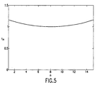
- Dielectric layers 13 1 ...13 N have optical thickness values which are quadratically chirped.
- Fig. 3 is a schematic representation of a fifteen layer stack, the optical thicknesses of the layers shown are not to scale.
- Fig. 4 illustrates exemplary optical thickness values (t n ) for each of the fifteen dielectric layers 13 1 ...13 15 included in stack 10. It should be understood that these thicknesses are provided for illustrative purposes only with respect to exemplary passbands.
- layers 13 1 and 13 15 have substantially the same optical thickness
- layers 13 2 and 13 14 also have substantially the same optical thickness and so on until layer 13 8 , which is the center layer and does not have a corresponding symmetric layer.
- n refers to the particular layer number in a stack and not to the layer number "m" within a cavity.
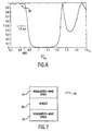
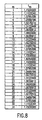
- FIG. 11 illustrates an exemplary transmission spectrum for the single cavity, 119 layer interference filter having the optical thickness values listed with reference to Fig. 10.
- a high transmission spike is present at approximately 1550nm while a relatively ripple-free transmission characteristic is present in the 1625nm range.
- a single cavity interference filter with a pair of quadratically chirped stacks provides high transmission at a first passband in the 1550nm range and at a second passband in the 1625nm range which can correspond to a payload channel wavelength and a service channel wavelength, respectively, within an optical network.
Landscapes
- Physics & Mathematics (AREA)
- General Physics & Mathematics (AREA)
- Optics & Photonics (AREA)
- Optical Filters (AREA)
Description


Claims (27)
- An optical interference filter comprising:characterised in that said plurality of first optical thicknesses and said plurality of second optical thicknesses vary quadratically in a first direction with respect to said substrate (12).a substrate (12) having a surface;a first stack (32) deposited on said surface of said substrate (12), said first stack (32) including a first plurality of dielectric layers (13N), each of selected ones of said first plurality of dielectric layers (13N) having a respective one of a plurality of first optical thicknesses;a second stack (33) including a second plurality of dielectric layers (13N), each of selected ones of said second plurality of dielectric layers (13N) having a respective one of a plurality of second optical thicknesses; anda spacer (35) interposed between said first (32) and second (33) stacks, said spacer (35) and said first (32) and second (33) stacks defining an optical cavity;
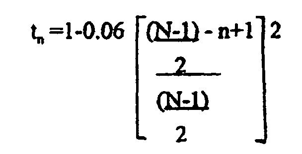
- The optical interference filter in accordance with claim 1 wherein said first plurality of optical thicknesses are determined based on a factor tn, said factor varying in accordance with:where N corresponds to a total number of said first plurality of dielectric layers (13N) and n corresponds to a particular one of said first plurality of dielectric layers (13N).

- The optical interference filter in accordance with claim 1 or 2 wherein said second plurality of optical thicknesses are determined based on a factor tn, said factor varying in accordance with:where N corresponds to a total number of said second plurality of dielectric layers (13N) and n corresponds to a particular one of said second plurality of dielectric layers (13N).
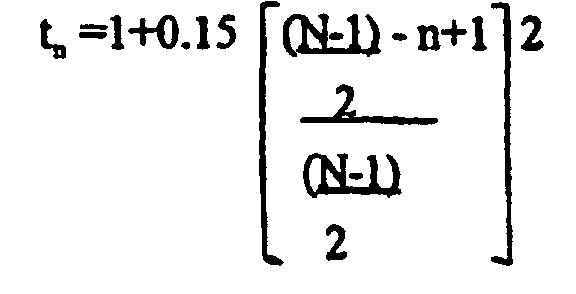
- The optical interference filter in accordance with claim 1 wherein said first plurality of optical thicknesses are determined based on a factor tn, said factor varying in accordance with:where N corresponds to a total number of said first plurality of dielectric layers (13N) and n corresponds to a particular one of said first plurality of dielectric layers (13N).

- The optical interference filter in accordance with claim 1 or 4, wherein said second plurality of optical thicknesses are determined based on a factor tn, said factor varying in accordance with:where N corresponds to a total number of said second plurality of dielectric layers (13N) and n corresponds to a particular one of said second plurality of dielectric layers (13N).
- The optical interference filter in accordance with any preceding claim, wherein each of said first plurality of dielectric layers (13N) comprises material of alternating high and low refractive index.
- The optical interference filter in accordance with any preceding claim, wherein each of said second plurality of dielectric layers (13N) comprises material of alternating high and low refractive index.
- The optical interference filter in accordance with any preceding claim, wherein said first plurality of dielectric layers (13N) are selected from the group consisting essentially of SiO2, Ta2O5, TiO2, Al2O3, HfO2, and ZrO2.
- The optical interference filter in accordance with any preceding claim, wherein said second plurality of dielectric layers (13N) are selected from the group consisting essentially of SiO2, Ta2O5, TiO2, Al2O3, HfO2, and ZrO2.
- The optical interference filter in accordance with any preceding claim, wherein said spacer (35) is formed of a dielectric material having a low refractive index.
- The optical interference filter in accordance with any preceding claim, wherein said filter has an associated transmission characteristic comprising first and second passbands.
- The optical interference filter in accordance with claim 11 wherein said first passband includes at least one optical channel having a wavelength in the 1.5µm range.
- The optical interference filter in accordance with claim 11 or 12, wherein said second passband includes at least one optical channel having a wavelength in the 1.3µm range.
- The optical interference filter in accordance with claim 11 or 12, wherein said second passband includes at least one optical channel having a wavelength in the 1.6µm range.
- A multi cavity optical interference filter comprising:characterised in that said first plurality of optical thicknesses vary quadratically over a first group of said first plurality of dielectric layers and said second plurality of optical thicknesses vary over a second group of said second plurality of dielectric layers.a plurality of cavities, each of said cavities being separated by a coupling layer, each of said plurality of cavities comprising:a first stack (32) including a first plurality of dielectric layers (13N), each of selected ones of said first plurality of dielectric layers having a respective one of a plurality of first optical thicknesses;a second stack (33) including a second plurality of dielectric layers (13N), each of selected ones of said second plurality of dielectric layers having a respective one of a plurality of second optical thicknesses; anda spacer (35) interposed between said first (32) and second (33) stacks, said spacer (35) and said first (32) and second (33) stacks defining a respective one of said plurality of cavities;
- The multi cavity interference filter in accordance with claim 15 wherein said first plurality of optical thicknesses are determined based on a factor tn, said factor varying in accordance with:where N corresponds to a total number of said first plurality of dielectric layers (13N) and n corresponds to a particular one of said first plurality of dielectric layers (13N).

- The optical interference filter in accordance with claim 15 or 16 wherein said second plurality of optical thicknesses are determined based on a factor tn, said factor varying in accordance with:where N corresponds to a total number of said second plurality of dielectric layers (13N) and n corresponds to a particular one of said second plurality of dielectric layers (13N).

- The optical interference filter in accordance with claim 1 5 wherein said first plurality of optical thicknesses are determined based on a factor tn, said factor varying in accordance with:where N corresponds to a total number of said first plurality of dielectric layers (13N) and n corresponds to a particular one of said first plurality of dielectric layers (13N).
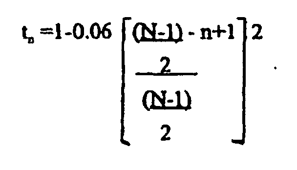
- The optical interference filter in accordance with claim 15 or 18 wherein said second plurality of optical thicknesses are determined based on a factor tn, said factor varying in accordance with:where N corresponds to a total number of said second plurality of dielectric layers (13N) and n corresponds to a particular one of said second plurality of dielectric layers (13N).

- The optical interference filter in accordance with any of claims 15 to 19 wherein each of said first plurality of dielectric layers (13N) comprises material of alternating high and low refractive index.
- The optical interference filter in accordance with any of claims 15 to 20 wherein each of said second plurality of dielectric layers (13N) comprises material of alternating high and low refractive index.
- The optical interference filter in accordance with any of claims 15 to 21 wherein each of said spacers (35) is formed of a dielectric material having a low refractive index.
- The optical interference filter in accordance with any of claims 15 to 22 wherein said filter has an associated transmission characteristic comprising a first and second passbands.
- The optical interference filter in accordance with claim 23 wherein said first passband includes at least one optical channel having a wavelength in the 1.5µm range.
- The optical interference filter in accordance with claim 23 or 24 wherein said second passband includes at least one optical channel having a wavelength in the 1.3µm range.
- The optical interference filter in accordance with any of claims 15 to 25 wherein said coupling layer is a material having a high index of refraction.
- The optical interference filter in accordance with any of claims 15 to 25 wherein said coupling layer is a material having a low index of refraction.
Applications Claiming Priority (3)
| Application Number | Priority Date | Filing Date | Title |
|---|---|---|---|
| US7153798P | 1998-01-15 | 1998-01-15 | |
| US71537P | 1998-01-15 | ||
| PCT/US1999/000836 WO1999036811A1 (en) | 1998-01-15 | 1999-01-14 | Optical interference filter |
Publications (2)
| Publication Number | Publication Date |
|---|---|
| EP0966696A1 EP0966696A1 (en) | 1999-12-29 |
| EP0966696B1 true EP0966696B1 (en) | 2004-05-26 |
Family
ID=22101963
Family Applications (1)
| Application Number | Title | Priority Date | Filing Date |
|---|---|---|---|
| EP99902266A Expired - Lifetime EP0966696B1 (en) | 1998-01-15 | 1999-01-14 | Optical interference filter |
Country Status (6)
| Country | Link |
|---|---|
| US (1) | US6301042B1 (en) |
| EP (1) | EP0966696B1 (en) |
| AU (1) | AU2228799A (en) |
| CA (1) | CA2285466A1 (en) |
| DE (1) | DE69917532T2 (en) |
| WO (1) | WO1999036811A1 (en) |
Families Citing this family (25)
| Publication number | Priority date | Publication date | Assignee | Title |
|---|---|---|---|---|
| US6590925B1 (en) * | 1999-11-01 | 2003-07-08 | Massachusetts Institute Of Technology | Double-chirped mirror systems and methods |
| JP3255638B1 (en) * | 2000-06-07 | 2002-02-12 | 日本板硝子株式会社 | Substrate for reflective liquid crystal display |
| JP2002171016A (en) * | 2000-11-30 | 2002-06-14 | Sumitomo Electric Ind Ltd | Optical filter, optical amplification system and optical communication system |
| US6844977B2 (en) | 2001-01-26 | 2005-01-18 | Ciena Corporation | Multi-channel optical filter |
| US6763046B2 (en) * | 2001-03-01 | 2004-07-13 | Applied Optoelectronics, Inc. | Method and system employing multiple reflectivity band reflector for laser wavelength monitoring |
| WO2002075378A2 (en) * | 2001-03-17 | 2002-09-26 | Marconi Uk Intellectual Property Ltd | Tuneable optical filter arrangement for wavelength division multiplex (wdm) network |
| US6618199B2 (en) * | 2001-06-05 | 2003-09-09 | Axsun Technologies, Inc. | Dual-band fabry-perot mirror coating |
| JP4187953B2 (en) | 2001-08-15 | 2008-11-26 | キャボットスーパーメタル株式会社 | Method for producing nitrogen-containing metal powder |
| US6728038B2 (en) | 2001-08-29 | 2004-04-27 | Jds Uniphase Corporation | Low chromatic dispersion filter for WDM |
| US6865315B2 (en) * | 2001-08-29 | 2005-03-08 | Jds Uniphase Corporation | Dispersion compensating filters |
| AU2003232487A1 (en) * | 2002-04-19 | 2003-11-03 | Katana Technologies Gmbh | Production of laser radiation with a low bandwidth for frequency conversion |
| US7276699B2 (en) | 2005-05-18 | 2007-10-02 | Northrop Grumman Corporation | Absorptance enhancing coating for MWIR detectors |
| US7588866B2 (en) | 2005-06-01 | 2009-09-15 | Kinoptics Technologies Inc. | Filter arrays for liquid crystal displays and methods of making the same |
| US7759644B2 (en) * | 2008-03-18 | 2010-07-20 | Drs Rsta, Inc. | Spectrally tunable infrared image sensor having multi-band stacked detectors |
| DE102009026449B4 (en) | 2009-05-25 | 2014-04-30 | Universität Kassel | Optical thin film structure with a distributed cavity |
| US8847177B2 (en) * | 2009-11-24 | 2014-09-30 | Koninklijke Philips N.V. | Luminescent solar concentrator |
| JP5625614B2 (en) * | 2010-08-20 | 2014-11-19 | セイコーエプソン株式会社 | Optical filter, optical filter module, spectrophotometer and optical instrument |
| CN105589221B (en) * | 2016-03-04 | 2018-04-03 | 北京航空航天大学 | A kind of tunable dual-passband microwave photon filter based on stimulated Brillouin scattering |
| US10819922B2 (en) * | 2017-02-21 | 2020-10-27 | Nanolux Co. Ltd. | Solid-state imaging element and imaging device |
| US10782460B2 (en) | 2017-05-22 | 2020-09-22 | Viavi Solutions Inc. | Multispectral filter |
| US11153514B2 (en) * | 2017-11-30 | 2021-10-19 | Brillnics Singapore Pte. Ltd. | Solid-state imaging device, method for driving solid-state imaging device, and electronic apparatus |
| US11143803B2 (en) | 2018-07-30 | 2021-10-12 | Viavi Solutions Inc. | Multispectral filter |
| CN112912773B (en) | 2018-11-06 | 2024-03-15 | 富士胶片株式会社 | Imaging lenses and imaging devices |
| CN118190157A (en) | 2019-03-06 | 2024-06-14 | 松下知识产权经营株式会社 | Light detection device, light detection system and filter array |
| CN119126284B (en) * | 2024-04-08 | 2025-05-30 | 上海泊睿科学仪器有限公司 | Optical filter for material photo-aging test and plating method and application thereof |
Family Cites Families (17)
| Publication number | Priority date | Publication date | Assignee | Title |
|---|---|---|---|---|
| JPS6038683B2 (en) * | 1981-06-24 | 1985-09-02 | キヤノン株式会社 | trimming filter |
| US4501470A (en) * | 1981-09-28 | 1985-02-26 | Rockwell International Corporation | Christiansen-Bragg optical filter |
| JPS6318304A (en) * | 1986-07-11 | 1988-01-26 | Matsushita Electric Ind Co Ltd | Bandpass filter for separating two wavelengths |
| US4756602A (en) * | 1987-06-05 | 1988-07-12 | Rockwell International Corporation | Narrowband optical filter with partitioned cavity |
| US4958892A (en) * | 1988-10-18 | 1990-09-25 | Physical Optics Corporation | Diffraction coherence filter |
| JPH02170101A (en) * | 1988-12-23 | 1990-06-29 | Minolta Camera Co Ltd | Interference filter |
| FR2658619B1 (en) | 1990-02-19 | 1993-04-02 | Megademini Taoufik | MULTIFRACTAL INTERFERENTIAL MIRRORS WITH FRACTAL DIMENSIONS BETWEEN 0 AND 1. |
| US5099359A (en) * | 1990-09-11 | 1992-03-24 | Eastman Kodak Company | Composite optical interference filter for use in film scanner system |
| US5360659A (en) | 1993-05-24 | 1994-11-01 | The Dow Chemical Company | Two component infrared reflecting film |
| US5410431A (en) | 1993-06-01 | 1995-04-25 | Rockwell International Corporation | Multi-line narrowband-pass filters |
| HU214659B (en) * | 1993-08-23 | 1998-04-28 | Szilárdtestfizikai Kutatóintézet | Dispersive dielectric mirror and method of design of the same |
| US5664124A (en) * | 1994-11-30 | 1997-09-02 | International Business Machines Corporation | Bridge between two buses of a computer system that latches signals from the bus for use on the bridge and responds according to the bus protocols |
| US6018421A (en) * | 1995-06-28 | 2000-01-25 | Cushing; David Henry | Multilayer thin film bandpass filter |
| US5999322A (en) * | 1995-06-28 | 1999-12-07 | Cushing; David Henry | Multilayer thin film bandpass filter |
| US5777793A (en) * | 1996-07-25 | 1998-07-07 | Northern Telecom Limited | Polarization insensitive multilayer planar reflection filters with near ideal spectral response |
| US5912915A (en) * | 1997-05-19 | 1999-06-15 | Coherent, Inc. | Ultrafast laser with multiply-folded resonant cavity |
| CA2238606A1 (en) * | 1997-06-26 | 1998-12-26 | Michael Anthony Scobey | Cascaded optical multiplexing devices |
-
1999
- 1999-01-14 DE DE69917532T patent/DE69917532T2/en not_active Expired - Fee Related
- 1999-01-14 AU AU22287/99A patent/AU2228799A/en not_active Abandoned
- 1999-01-14 US US09/232,133 patent/US6301042B1/en not_active Expired - Lifetime
- 1999-01-14 CA CA002285466A patent/CA2285466A1/en not_active Abandoned
- 1999-01-14 WO PCT/US1999/000836 patent/WO1999036811A1/en not_active Ceased
- 1999-01-14 EP EP99902266A patent/EP0966696B1/en not_active Expired - Lifetime
Also Published As
| Publication number | Publication date |
|---|---|
| WO1999036811A1 (en) | 1999-07-22 |
| DE69917532D1 (en) | 2004-07-01 |
| DE69917532T2 (en) | 2005-06-30 |
| US6301042B1 (en) | 2001-10-09 |
| CA2285466A1 (en) | 1999-07-22 |
| AU2228799A (en) | 1999-08-02 |
| EP0966696A1 (en) | 1999-12-29 |
Similar Documents
| Publication | Publication Date | Title |
|---|---|---|
| US6301042B1 (en) | Fabry-perot optical filter with chirped dielectric mirrors | |
| US6407863B1 (en) | Dual transmission band interference filter | |
| US8989537B2 (en) | Highly efficient optical gratings with reduced thickness requirements and impedance-matching layers | |
| CA2220291C (en) | Multilayer thin film dielectric bandpass filter | |
| US6215592B1 (en) | Fabry-perot optical filter and method of making the same | |
| US6666944B2 (en) | Method of manufacturing optical filter | |
| EP1408350A1 (en) | Multi-cavity optical filter | |
| US20050068541A1 (en) | Partitioned-cavity tunable fabry-perot filter | |
| KR20010099801A (en) | Optical multiplexer/demultiplexer using resonant grating filters | |
| US7145722B2 (en) | Optical filter and method of manufacturing thereof | |
| US4929063A (en) | Nonlinear tunable optical bandpass filter | |
| US6600604B2 (en) | Athermal thin film filter | |
| US7333266B2 (en) | CWDM filter | |
| US6844977B2 (en) | Multi-channel optical filter | |
| WO2000063728A9 (en) | Dual transmission band interference filter | |
| US7355792B2 (en) | CWDM filter for eliminating noise | |
| US20080107874A1 (en) | Optical element including dielectric multilayer film and manufacturing method thereof | |
| US20040017973A1 (en) | Wavelength filter, variable wavelength filter, and optical device | |
| RU2079861C1 (en) | Band-pass light filter | |
| US20060147212A1 (en) | Optical filter, an optical interleaver and associated methods of manufacture | |
| JPS59127007A (en) | Dichroic filter |
Legal Events
| Date | Code | Title | Description |
|---|---|---|---|
| PUAI | Public reference made under article 153(3) epc to a published international application that has entered the european phase |
Free format text: ORIGINAL CODE: 0009012 |
|
| 17P | Request for examination filed |
Effective date: 19991006 |
|
| AK | Designated contracting states |
Kind code of ref document: A1 Designated state(s): BE DE FR GB IT NL SE |
|
| 17Q | First examination report despatched |
Effective date: 20030425 |
|
| GRAP | Despatch of communication of intention to grant a patent |
Free format text: ORIGINAL CODE: EPIDOSNIGR1 |
|
| GRAS | Grant fee paid |
Free format text: ORIGINAL CODE: EPIDOSNIGR3 |
|
| GRAA | (expected) grant |
Free format text: ORIGINAL CODE: 0009210 |
|
| AK | Designated contracting states |
Kind code of ref document: B1 Designated state(s): BE DE FR GB IT NL SE |
|
| PG25 | Lapsed in a contracting state [announced via postgrant information from national office to epo] |
Ref country code: NL Free format text: LAPSE BECAUSE OF FAILURE TO SUBMIT A TRANSLATION OF THE DESCRIPTION OR TO PAY THE FEE WITHIN THE PRESCRIBED TIME-LIMIT Effective date: 20040526 Ref country code: BE Free format text: LAPSE BECAUSE OF FAILURE TO SUBMIT A TRANSLATION OF THE DESCRIPTION OR TO PAY THE FEE WITHIN THE PRESCRIBED TIME-LIMIT Effective date: 20040526 |
|
| REG | Reference to a national code |
Ref country code: GB Ref legal event code: FG4D |
|
| REF | Corresponds to: |
Ref document number: 69917532 Country of ref document: DE Date of ref document: 20040701 Kind code of ref document: P |
|
| PG25 | Lapsed in a contracting state [announced via postgrant information from national office to epo] |
Ref country code: SE Free format text: LAPSE BECAUSE OF FAILURE TO SUBMIT A TRANSLATION OF THE DESCRIPTION OR TO PAY THE FEE WITHIN THE PRESCRIBED TIME-LIMIT Effective date: 20040826 |
|
| NLV1 | Nl: lapsed or annulled due to failure to fulfill the requirements of art. 29p and 29m of the patents act | ||
| PGFP | Annual fee paid to national office [announced via postgrant information from national office to epo] |
Ref country code: FR Payment date: 20050117 Year of fee payment: 7 |
|
| ET | Fr: translation filed | ||
| PLBE | No opposition filed within time limit |
Free format text: ORIGINAL CODE: 0009261 |
|
| STAA | Information on the status of an ep patent application or granted ep patent |
Free format text: STATUS: NO OPPOSITION FILED WITHIN TIME LIMIT |
|
| 26N | No opposition filed |
Effective date: 20050301 |
|
| PGFP | Annual fee paid to national office [announced via postgrant information from national office to epo] |
Ref country code: DE Payment date: 20060117 Year of fee payment: 8 |
|
| PG25 | Lapsed in a contracting state [announced via postgrant information from national office to epo] |
Ref country code: FR Free format text: LAPSE BECAUSE OF NON-PAYMENT OF DUE FEES Effective date: 20060131 |
|
| PGFP | Annual fee paid to national office [announced via postgrant information from national office to epo] |
Ref country code: IT Payment date: 20060131 Year of fee payment: 8 |
|
| REG | Reference to a national code |
Ref country code: FR Ref legal event code: ST Effective date: 20060929 |
|
| PG25 | Lapsed in a contracting state [announced via postgrant information from national office to epo] |
Ref country code: DE Free format text: LAPSE BECAUSE OF NON-PAYMENT OF DUE FEES Effective date: 20070801 |
|
| PGFP | Annual fee paid to national office [announced via postgrant information from national office to epo] |
Ref country code: GB Payment date: 20090114 Year of fee payment: 11 |
|
| PG25 | Lapsed in a contracting state [announced via postgrant information from national office to epo] |
Ref country code: IT Free format text: LAPSE BECAUSE OF NON-PAYMENT OF DUE FEES Effective date: 20070114 |
|
| GBPC | Gb: european patent ceased through non-payment of renewal fee |
Effective date: 20100114 |
|
| PG25 | Lapsed in a contracting state [announced via postgrant information from national office to epo] |
Ref country code: GB Free format text: LAPSE BECAUSE OF NON-PAYMENT OF DUE FEES Effective date: 20100114 |