EP0964571A2 - "Electronic devices comprising an array" - Google Patents
"Electronic devices comprising an array" Download PDFInfo
- Publication number
- EP0964571A2 EP0964571A2 EP99202981A EP99202981A EP0964571A2 EP 0964571 A2 EP0964571 A2 EP 0964571A2 EP 99202981 A EP99202981 A EP 99202981A EP 99202981 A EP99202981 A EP 99202981A EP 0964571 A2 EP0964571 A2 EP 0964571A2
- Authority
- EP
- European Patent Office
- Prior art keywords
- row
- voltage
- column
- diodes
- magnitude
- Prior art date
- Legal status (The legal status is an assumption and is not a legal conclusion. Google has not performed a legal analysis and makes no representation as to the accuracy of the status listed.)
- Granted
Links
Images


Classifications
-
- G—PHYSICS
- G06—COMPUTING; CALCULATING OR COUNTING
- G06F—ELECTRIC DIGITAL DATA PROCESSING
- G06F3/00—Input arrangements for transferring data to be processed into a form capable of being handled by the computer; Output arrangements for transferring data from processing unit to output unit, e.g. interface arrangements
- G06F3/14—Digital output to display device ; Cooperation and interconnection of the display device with other functional units
- G06F3/147—Digital output to display device ; Cooperation and interconnection of the display device with other functional units using display panels
-
- H—ELECTRICITY
- H04—ELECTRIC COMMUNICATION TECHNIQUE
- H04N—PICTORIAL COMMUNICATION, e.g. TELEVISION
- H04N25/00—Circuitry of solid-state image sensors [SSIS]; Control thereof
- H04N25/70—SSIS architectures; Circuits associated therewith
- H04N25/76—Addressed sensors, e.g. MOS or CMOS sensors
- H04N25/767—Horizontal readout lines, multiplexers or registers
-
- H—ELECTRICITY
- H04—ELECTRIC COMMUNICATION TECHNIQUE
- H04N—PICTORIAL COMMUNICATION, e.g. TELEVISION
- H04N25/00—Circuitry of solid-state image sensors [SSIS]; Control thereof
- H04N25/70—SSIS architectures; Circuits associated therewith
- H04N25/76—Addressed sensors, e.g. MOS or CMOS sensors
Definitions
- This invention relates to electronic devices, particularly but not exclusively with thin-film circuitry, comprising an array of device elements and having column multiplexer circuits.
- the device elements produce currents flowing in the columns of the arrays, and may be image sensor elements, for example photosensitive diodes, of a large area image sensor, or other types of device element, for example temperature sensing elements of a thermal imaging device.
- diode bridges of the column multiplexer circuits for different groups of the column conductors are highly preferred for the diode bridges of the column multiplexer circuits for different groups of the column conductors to share common control lines, so as to reduce the number of such control lines in the device.
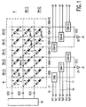
- the electronic device of Figures 1 and 2 comprises an array 1 of device elements 2 and 3 which are arranged in rows N, (N+1), across and columns M, (M+1), notably and which are coupled to row and column conductors A and B respectively.
- the column conductors B are arranged in groups, such as group B(M), B(M+1), B(M+2) and the group B(M+3), B(M+4), B(M+5). Each such group has a respective common terminal 5.
- a column multiplexer circuit C(M), C(M+1), Vietnamese couples the column conductors B of a respective group to the respective common terminal 5(1), 5(2), .
- Figures 6 and 7 show row pulse waveforms to be applied to the row conductor 6 in order to address the elements of a row, and which enable the peak current flowing through the column conductors B to be reduced with the result that the current which must be supplied by the current sources 21 and 22 can be reduced.
- line-scan pulses serve for forward-biasing the switching diodes 3 of the addressed row.
- the invention is also concerned with the form of the line scan pulses, as will be described in the following.
- the photo-generated signal from those photosensitive diodes 2 whose switching diodes are forward biased is read out on their column conductor B via their respective column multiplexer circuit C.
- a charge-sensitive amplifier 35 is connected to the common terminal 5 to read this photo-generated signal in known manner.
- the charge-sensitive amplifiers 35 may be formed as monolithic silicon integrated circuits, separate from the device substrate 40 on which the array 1 and column multiplexer circuits C may be formed by thin-film circuitry.
- the common terminals 5 may be output terminals of the device substrate 40.
- the row driver 36 may be formed in monolithic silicon integrated circuit technology (separate from the device substrate 40), and so the connections 6 between the row driver 36 and the row conductors A may also be output terminals of the device substrate 40.
- these circuit parts may be formed on the same device substrate 40 as the array 1, in which case the terminals 5 and 6 would be internal circuit nodes of the thin-film circuitry on the device substrate 40.
- the column multiplexer circuits C(M) and C(M+3), etc Vietnamese for the different groups of the column conductors B share common control lines 16 and 17 (Vx1, Vy1, Vx2, Vy2 ...) so as to reduce the number of such control lines in the layout of the device substrate 40.
- These separate control lines 16 and 17 may extend to output terminals on the device substrate, or they may be connected to a control circuit formed in thin-film circuitry on the same device substrate 40.
- the control circuit (either integrated on the device substrate 40 or formed as an external monolithic integrated circuit) generates sequences of voltage pulses Vx and Vy for switching the column multiplexer circuits sequentially within each group.
- Figure 2 illustrates the circuit construction of each column multiplexer C.
- the circuit components of the multiplexer are chosen to be of the same technology type as the device elements of the array 1.
- thin-film diodes are used for both the multiplexer circuit C and for the array 1. All these diodes may be fabricated simultaneously on the device substrate 40 using the same processing steps.
- Vx positive (e.g. +5V)
- Vy negative (e.g. -5V)
- the switching diodes SD1 and SD2 act as a voltage clamp, clamping the column conductor B at a constant potential.
- the clamping effect can best be understood by considering the device elements 2,3 of the various rows which are coupled to this column conductor B.
- the multiplexer C of Figure 2 may be C(M) of Figure 1, and the pixels of row N may be addressed by a positive voltage scanning pulse on row conductor 6(1).
- the switching diode 3 of row N, column M is forward biased, and the switching diodes 3 of all the other rows (N+1), (N+2),etc. in column M are reverse biased.
- clamping switch may comprise one or more thin-film transistors.
- the clamping switch may be an insulated-gate thin-film transistor which has its source and drain electrodes coupled between the respective column conductor and a reference voltage source. This transistor may be switched on and off, by a control signal applied to its insulated gate.
- a clamp line may extend across the columns of the device, and the clamping switch may be coupled between its respective column conductor and the clamp line which is at a reference voltage.
- the clamping switch is shown as integrated with the column multiplexer, but it may be coupled to the column conductor at a location remote from the diode bridge. In the example shown, the operation of the clamping switch is controlled by coupling it to the control lines of the respective diode bridge, but of course, the clamping switch may have independent control.
- the input current i i is the charging current which recharges the pixel photodiode self-capacitance. This charging current varies during the recharging operation, and also depends upon the level of illumination of the pixel photodiode during the integration period. As a consequence of equations (9) and (10), the photodiodes PD1 and PD2 must produce a current which is sufficient to at least equal the maximum capacitor charging current, and this imposes minimum dimensions for the photodiodes PD1 and PD2.
- the present invention provides a method of operating the multiplexer circuits so as to reduce the peak current flow which must be switched by the diode bridge network.
- the pitch between pixels is approximately 200 ⁇ m.
- the photodiode capacitance is relatively high, therefore resulting in large recharging currents.
- the following analysis is therefore based on assumptions which give rise to large recharging currents, representing a worst-case estimate.
- a 200 ⁇ m pixel pitch may allow the photodiode of each pixel to occupy an area of 140 ⁇ m x 140 ⁇ m.
- a typical thin film photodiode construction of this dimension will have a capacitance of approximately 4 pF.
- the row conductor When the row conductor is driven so as to select a respective row of pixels, the row conductor provides a current to recharge the photodiode self-capacitance, and this recharging current flows through the respective switching diode and into the column conductor B for measurement. It is the maximum value of this capacitor recharging current which determines the minimum currents that must be produced by the photodiodes PD1 and PD2 of the multiplexer circuits.
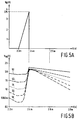
- Figure 4 shows the recharging characteristics for the photodiode capacitance using a conventional rectangular row waveform. As shown, the row waveform is pulsed high at 2.3ms (for the purposes of the simulation) and remains high for a duration of 0.1ms.
- the row voltage waveform VR is represented in part A of Figure 4, and the peak voltage is 3 volts.
- Figure 4 part B shows the voltage across the photodiode VPH for the situation where different light intensities have illuminated the photodiode between row pulses.
- the curve referenced 58 represents a maximum illumination of the pixel and consequently the photodiode capacitance is almost completely discharged at the end of the integration period (between row pulses).
- Curve 50 represents a low level of illumination of the photodiode and the curves 52 - 56 represent increasing levels of illumination.
- the photodiode capacitance is recharged so that the voltage across the photodiode increases.
- the photodiode voltage reaches a maximum which corresponds substantially to the voltage level of the row pulse less the forward bias voltage drop across the switching diode 3 (assuming that respective column conductor is held at 0 volts during readout).
- the voltage across the photodiode drops in dependence upon the level of illumination. It should be noted that the rate at which the voltage is shown to drop in Figure 4 is exaggerated for the purposes of illustration since the time between row pulses is significantly greater than the duration of the row pulse. For example, in the case of an A4 image scanner, if a resolution of 125dpi is achieved, this represents approximately 1,000 rows so that each row pulse lasts 0.1ms and is repeated every 100 ms.
- An amorphous silicon diode with an intrinsic layer depth of 5000 angstroms produces a current of 0.68 x 10 -15 A/ ⁇ m 2 /Lux (for light of 580nm wavelength).
- the light receptive area of the photodiode needs to be 14.7 x 10 6 ( ⁇ m) 2 .
- the pixel pitch defines the maximum separation of the photodiodes, although the photodiodes may be arranged alternately at opposite edges of the substrate.
- the maximum separation of the photodiodes for a 200 ⁇ m pixel pitch is 400 ⁇ m. To obtain the required area of photodiode to produce the 1 ⁇ A current, this maximum separation corresponds to a photodiode length of 37mm.
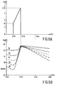
- Figure 6 shows the analysis for an alternative row select pulse, in which the row waveform has a stepped component and a ramped (saw tooth) component.
- a charging characteristic can be obtained for which the maximum charging current is at its lowest.
- the lowest peak charging current will be obtained when the maximum illumination curve 58 rises uniformly to the charged level during the row select period.
- the row waveform shown in Figure 6 part A achieves approximately this charging characteristic for the charging curve 58.
- the slope of this curve corresponds to a peak current of approximately 90 nA, and the corresponding required length of the multiplexer photodiode PD1 and PD2 is then 3.3 mm.
- FIG 7 illustrates one specific example of a multiplexer circuit C in accordance with the invention and fabricated in thin-film technology.
- This thin-film technology may be the same as that used to fabricate the array 1, and so it may be similar to that described in EP-A-0 633 542.
- the thin-film circuitry is formed on a substrate 40.
- This substrate 40 may be formed of any suitable glass or plastics material.
- a first electrically conductive layer 41 (for example of chromium) is deposited onto the substrate 40 and patterned by etching to define the cathode electrodes of the diodes PD1, PD2, SD1, SD2, SD3, SD4, etc ....
- This conductor pattern 41 may also form conductor tracks, for example for the lines 16 and 17, and also circuit nodes such as 13, 14, 15, 18 and 19.
- the various diode structures are then formed by depositing and patterning appropriately-doped semiconductor layers.
- all the diodes may be amorphous silicon n-i-p diodes formed by depositing in sequence n-type conductivity, intrinsic and p-type conductivity amorphous silicon layers 42 to 44. These layers 42 to 44 are patterned by etching to form a separate island for each diode. An insulating layer (for example silicon nitride) is then deposited and patterned so as to be left on the side-walls of the diode islands. This insulating layer pattern 45 leaves exposed at least of the top surface of the diode islands.
- insulating layer for example silicon nitride
- a second conductive layer 46 (for example chromium, possibly covered with aluminium) is then deposited and patterned to form the anode electrodes of the diodes and interconnections between the two conductive layer levels as desired.
- This top conductive layer 46 may be opaque to the illuminating light, in which case (as shown in Figure 4) the layer 46 may be restricted to the edge of the top p-type layer 44 of the photosensitive diodes PD1, PD2.
- the layer 46 extends, however, over the whole of the top of the switching diodes SD1 to SD6, so that these diodes are not photosensitive.
- the layout of the image sensor may have any appropriate configuration and pattern.
- the photodiodes PD1 and PD2 which act as the current sources of the multiplexer circuits C are located in an area of the device substrate 40 where they can be constantly exposed (during operation of the sensor device) to illumination of constant intensity.
- the switching diodes SD1 to SD6 are however shielded from this constant illumination by opaque electrode layers 41 and 46 and/or by an optical mask.
- the image array 1 is located in the area of the device substrate 40 where an image is to be sensed by the photodiodes 2.
- the row and column conductors A and B may define rectangular or square areas for the pixels, or any other desired geometry.
- the photodiodes 2 may occupy most of the pixel area.
- the photodiodes 2 may be confined to one or more edges of their respective pixel so as to allow the image sensor to be as transparent as possible. Such a transparent image sensor may then be placed on top of something else, such as a display, without significantly obscuring the display.
- Figure 7 illustrates an arrangement in which the light is incident at the top surface of the device and is transmitted to the semiconductor material of the photodiodes via windows in the top electrode layer 46.
- an inverted arrangement may be constructed in which the windows are present in the bottom electrode layer 41, and the incident light (for PD1 and PD2) and image (for array photodiodes 2) is transmitted via a transparent substrate 40.
- Figures 2 and 3 show single diodes SD3 to SD6 in each arm of the bridge, single diodes SD1 and SD2 between the column conductor and the respective control line 16, 17, and single diodes PD1 and PD2 forming the current sources 21 and 22.
- two diodes or more in series may be used instead of these single diodes.
- some imbalance may be present in the conduction characteristics of the diodes, and the diode and biasing arrangement may be such that the column conductor is operated at a potential which is not zero volts.
- the device elements of the array 1 may comprise thin-film transistors.
- each pixel may comprise a known circuit configuration of two switching transistors and a photoconductor.
- the diodes PD1, PD2, and SD1 to SD6 of the column multiplexer C may be formed as diode-connected thin-film transistors, i.e. the gate and drain of the transistor may be coupled together as one electrode of the circuit element.
- the clamping switch may be a single transistor having its source coupled to the conductor B, its drain coupled to a clamping voltage line, and its gate coupled to a control line for switching the transistor ON and OFF in opposite synchronisation with the diode bridge SD3 to SD6.
- An image sensor in accordance with the present invention may be designed as a document scanner.
- a very large area image sensor may be formed capable of scanning an A4 size page at a resolution of 300 dpi (dots per inch).
- the number of rows N, (N+1), ... and column M, (M+1), ... required for such an image sensor is about 2500 and 3500 respectively (with the rows parallel to the long side of the A4 page).
- the present invention permits the number of column outputs 5 to be reduced by grouping the column conductors B with column multiplexer circuits C in accordance with the present invention.
- a similar multiplexer circuit may be used on each row conductor A to reduce the number of inputs 6 from the row driver circuit 36.
- the multiplexer circuits C may be combined with other additional measures to reduce the number of row and column conductors A and B and input and output terminals 6 and 5.
- the array configuration may be similar to that disclosed in pending United Kingdom patent application GB 9505305.4 (our reference PHB 33976), in which the pixels are arranged in groups of four which share a common row conductor A and a common column conductor B.
- Memory arrays also comprising n-i-p or p-i-p diodes are known, for example as described in United States patent US-A-5,272,370 (our reference PHB 33725), the whole contents of which are incorporated herein as reference material.
- the column multiplexer circuits C in accordance with the present invention may be included between the read-out circuit and the column conductors B for switching/transmitting the digital data signals from an addressed row of the memory array 1.
- the array 1 and multiplexer circuits C of an electronic device in accordance with the present invention may be realised with monolithic silicon integrated circuit technology instead of thin-film circuitry.
Abstract
Description
- iso
- is the current generated by PD1
- isi
- is the current sunk by PD2
- ix
- is the bridge current flowing between nodes 18 and 13
- iy
- is the bridge current flowing between nodes 13 and 19
- iz
- is the bridge current flowing between nodes 18 and 14
- iw
- is the bridge current flowing between nodes 14 and 19
Claims (11)
- An electronic device comprising:an array of charge storage elements which are arranged in rows and columns and which are coupled to row and column conductors, a row signal applied to a row conductor enabling charge storage element signals of elements in the respective row to be supplied to the respective column conductors, the charge storage element signals producing a current flowing in the respective column conductors, the column conductors being arranged in at least one group, each group having a respective common terminal;a column multiplexer circuit coupling the column conductors of a respective group to the respective common terminal, in which the column multiplexer circuit for each column conductor comprises a respective diode bridge having first and second arms between two current sources, each arm comprising a respective pair of diodes coupled together at a respective node of that arm and having the same polarity as each other between the current sources, the respective column conductor being coupled to the node of the first arm, the common terminal being coupled to the node of the second arm;control lines coupled to the diode bridge for applying switching voltages for switching the diodes between forward bias in a first state of the bridge and reverse bias in a second state of the bridge, whereby a signal is transmitted between the column conductor and the common terminal in the first state of the diode bridge; andmeans for generating a row signal in the form of a base voltage which is interrupted by a pulse voltage waveform which rises in magnitude, relatively to the base voltage, from a first voltage magnitude immediately following the beginning of the pulse to a second voltage magnitude immediately preceding the end of the pulse.
- An electronic device as claimed in claim 1, wherein the means for generating a row signal is for generating a row signal in the form of a base voltage which is interrupted by a pulse voltage waveform which rises in magnitude, relatively to the base voltage, from the base voltage to the first voltage magnitude at the beginning of the row pulse, and falls in magnitude, relatively to the base voltage, from the second voltage magnitude to the base voltage at the end of the row pulse.
- An electronic device as claimed in claim 1 or 2, wherein the row signal magnitude rises uniformly from the first voltage magnitude to the second voltage magnitude.
- An electronic device as claimed in any preceding claim, wherein the device elements of the array comprise diodes of the same technology type as the diodes of the column multiplexer circuits.
- An electronic device according to claim 4, wherein the current sources of the column multiplexer circuits comprise photosensitive diodes of the same technology type as non-photosensitive diodes which form the diodes in the first and second arms of the bridge.
- An electronic device according to claim 4 or 5, wherein the diodes of the array and of the column multiplexer circuits are in the form of thin-film diodes on a common substrate.
- An electronic device as claimed in any preceding claim, wherein the column multiplexer circuits transmit analog signals between the column conductors and the common terminal in the first state of the diode bridge.
- An electronic device according to claim 7, wherein the device elements of the array are photosensitive diodes which together form an image sensor.
- A method of operating a device as claimed in any preceding claim comprising supplying a row voltage waveform to a row of charge storage elements, thereby enabling a signal to be transmitted from the elements of that row to the respective column conductors, and operating the column multiplexer circuits to transmit selected column signals to the respective common terminals, in which the row voltage waveform comprises a signal in the form of a base voltage which is interrupted by a pulse voltage waveform which rises in magnitude, relatively to the base voltage, from a first voltage magnitude immediately following the beginning of the pulse to a second voltage magnitude immediately preceding the end of the pulse
- A method as claimed in claim 9, wherein the pulse voltage waveform rises in magnitude, relatively to the base voltage, from the base voltage to the first voltage magnitude at the beginning of the row pulse, and falls in magnitude, relatively to the base voltage, from the second voltage magnitude to the base voltage at the end of the row pulse.
- A method as claimed in claim 10 or 11 wherein the row signal magnitude rises uniformly from the first voltage magnitude to the second voltage magnitude.
Applications Claiming Priority (5)
| Application Number | Priority Date | Filing Date | Title |
|---|---|---|---|
| GBGB9512942.5A GB9512942D0 (en) | 1995-06-24 | 1995-06-24 | Electronic devices comprising an array |
| GB9512942 | 1995-06-24 | ||
| GBGB9526159.0A GB9526159D0 (en) | 1995-06-24 | 1995-12-21 | Electronic devices comprising an array |
| GB9526159 | 1995-12-21 | ||
| EP96916276A EP0777945B1 (en) | 1995-06-24 | 1996-06-21 | Electronic devices comprising an array |
Related Parent Applications (1)
| Application Number | Title | Priority Date | Filing Date |
|---|---|---|---|
| EP96916276.7 Division | 1997-01-16 |
Publications (3)
| Publication Number | Publication Date |
|---|---|
| EP0964571A2 true EP0964571A2 (en) | 1999-12-15 |
| EP0964571A3 EP0964571A3 (en) | 2003-05-14 |
| EP0964571B1 EP0964571B1 (en) | 2004-10-27 |
Family
ID=10776660
Family Applications (1)
| Application Number | Title | Priority Date | Filing Date |
|---|---|---|---|
| EP99202981A Expired - Lifetime EP0964571B1 (en) | 1995-06-24 | 1996-06-21 | Electronic devices comprising an array |
Country Status (3)
| Country | Link |
|---|---|
| EP (1) | EP0964571B1 (en) |
| KR (1) | KR100392860B1 (en) |
| GB (2) | GB9512942D0 (en) |
Cited By (1)
| Publication number | Priority date | Publication date | Assignee | Title |
|---|---|---|---|---|
| EP1241456A2 (en) * | 2001-03-12 | 2002-09-18 | Infrared Integrated Systems Ltd. | A method of multiplexing column amplifiers in a resistive bolometer array |
Citations (2)
| Publication number | Priority date | Publication date | Assignee | Title |
|---|---|---|---|---|
| US4518921A (en) * | 1982-10-18 | 1985-05-21 | At&T Bell Laboratories | Track and hold circuit |
| EP0633542A2 (en) * | 1993-07-05 | 1995-01-11 | Philips Electronics Uk Limited | An electro-optic device |
-
1995
- 1995-06-24 GB GBGB9512942.5A patent/GB9512942D0/en active Pending
- 1995-12-21 GB GBGB9526159.0A patent/GB9526159D0/en active Pending
-
1996
- 1996-06-21 KR KR1019970701408A patent/KR100392860B1/en not_active IP Right Cessation
- 1996-06-21 EP EP99202981A patent/EP0964571B1/en not_active Expired - Lifetime
Patent Citations (2)
| Publication number | Priority date | Publication date | Assignee | Title |
|---|---|---|---|---|
| US4518921A (en) * | 1982-10-18 | 1985-05-21 | At&T Bell Laboratories | Track and hold circuit |
| EP0633542A2 (en) * | 1993-07-05 | 1995-01-11 | Philips Electronics Uk Limited | An electro-optic device |
Cited By (3)
| Publication number | Priority date | Publication date | Assignee | Title |
|---|---|---|---|---|
| EP1241456A2 (en) * | 2001-03-12 | 2002-09-18 | Infrared Integrated Systems Ltd. | A method of multiplexing column amplifiers in a resistive bolometer array |
| EP1241456A3 (en) * | 2001-03-12 | 2002-12-18 | Infrared Integrated Systems Ltd. | A method of multiplexing column amplifiers in a resistive bolometer array |
| US6809595B2 (en) | 2001-03-12 | 2004-10-26 | Infrared Integrated Systems Limited | Method of multiplexing column amplifiers in a resistive bolometer array |
Also Published As
| Publication number | Publication date |
|---|---|
| GB9526159D0 (en) | 1996-02-21 |
| EP0964571B1 (en) | 2004-10-27 |
| GB9512942D0 (en) | 1995-08-30 |
| KR100392860B1 (en) | 2003-10-30 |
| EP0964571A3 (en) | 2003-05-14 |
| KR970705788A (en) | 1997-10-09 |
Similar Documents
| Publication | Publication Date | Title |
|---|---|---|
| US5721422A (en) | Electronic devices having an array with shared column conductors | |
| EP0233489B1 (en) | Method of addressing at least one photosensitive pixel or liquid crystal pixel in a matrix array | |
| EP0777945B1 (en) | Electronic devices comprising an array | |
| US4495409A (en) | Photosensor with diode array | |
| EP0260824B1 (en) | Circuit for a photosensitive pixel with exposed blocking element | |
| EP0622851A1 (en) | Image sensor | |
| US6449014B1 (en) | Image sensor having a low impedance reading block between pixel data lines and output line | |
| US5608205A (en) | Imaging device having reduced vertical crosstalk | |
| EP0670657B1 (en) | A charge storage device | |
| EP0964571B1 (en) | Electronic devices comprising an array | |
| US5856666A (en) | Multiplexer circuit | |
| US6759889B2 (en) | Diode multiplexer circuit and electronic device incorporating the same | |
| US6545711B1 (en) | Photo diode pixel sensor array having a guard ring | |
| EP0670658B1 (en) | A charge storage device | |
| US5235174A (en) | Image sensor having dual shift registers and a plurality of capacitors | |
| JPH0628310B2 (en) | Photoelectric conversion device | |
| JPH0812907B2 (en) | Photoelectric conversion device | |
| JPH0654117A (en) | Image sensor and driving method therefor | |
| WO1998005122A1 (en) | Multiplexer circuit | |
| JPH0537714A (en) | Photoelectric converter | |
| KR930020703A (en) | Imaging Device and Imaging Device Array | |
| JPS6119149B2 (en) |
Legal Events
| Date | Code | Title | Description |
|---|---|---|---|
| PUAI | Public reference made under article 153(3) epc to a published international application that has entered the european phase |
Free format text: ORIGINAL CODE: 0009012 |
|
| AC | Divisional application: reference to earlier application |
Ref document number: 777945 Country of ref document: EP |
|
| AK | Designated contracting states |
Kind code of ref document: A2 Designated state(s): DE FR GB |
|
| AX | Request for extension of the european patent |
Free format text: AL PAYMENT 19991013;LT PAYMENT 19991013;LV PAYMENT 19991013;SI PAYMENT 19991013 |
|
| RTI1 | Title (correction) |
Free format text: ELECTRONIC DEVICES COMPRISING AN ARRAY |
|
| PUAL | Search report despatched |
Free format text: ORIGINAL CODE: 0009013 |
|
| AK | Designated contracting states |
Designated state(s): DE FR GB |
|
| AX | Request for extension of the european patent |
Extension state: AL LT LV SI |
|
| 17P | Request for examination filed |
Effective date: 20031114 |
|
| GRAP | Despatch of communication of intention to grant a patent |
Free format text: ORIGINAL CODE: EPIDOSNIGR1 |
|
| AKX | Designation fees paid |
Designated state(s): DE FR GB |
|
| AXX | Extension fees paid |
Extension state: SI Payment date: 19991013 Extension state: LV Payment date: 19991013 Extension state: LT Payment date: 19991013 Extension state: AL Payment date: 19991013 |
|
| GRAS | Grant fee paid |
Free format text: ORIGINAL CODE: EPIDOSNIGR3 |
|
| GRAA | (expected) grant |
Free format text: ORIGINAL CODE: 0009210 |
|
| AC | Divisional application: reference to earlier application |
Ref document number: 0777945 Country of ref document: EP Kind code of ref document: P |
|
| AK | Designated contracting states |
Kind code of ref document: B1 Designated state(s): DE FR GB |
|
| AX | Request for extension of the european patent |
Extension state: AL LT LV SI |
|
| REG | Reference to a national code |
Ref country code: GB Ref legal event code: FG4D |
|
| REG | Reference to a national code |
Ref country code: GB Ref legal event code: 746 Effective date: 20041101 |
|
| REF | Corresponds to: |
Ref document number: 69633745 Country of ref document: DE Date of ref document: 20041202 Kind code of ref document: P |
|
| ET | Fr: translation filed | ||
| PLBE | No opposition filed within time limit |
Free format text: ORIGINAL CODE: 0009261 |
|
| STAA | Information on the status of an ep patent application or granted ep patent |
Free format text: STATUS: NO OPPOSITION FILED WITHIN TIME LIMIT |
|
| 26N | No opposition filed |
Effective date: 20050728 |
|
| REG | Reference to a national code |
Ref country code: FR Ref legal event code: D6 |
|
| PGFP | Annual fee paid to national office [announced via postgrant information from national office to epo] |
Ref country code: FR Payment date: 20060627 Year of fee payment: 11 |
|
| PGFP | Annual fee paid to national office [announced via postgrant information from national office to epo] |
Ref country code: GB Payment date: 20060628 Year of fee payment: 11 |
|
| PGFP | Annual fee paid to national office [announced via postgrant information from national office to epo] |
Ref country code: DE Payment date: 20060811 Year of fee payment: 11 |
|
| GBPC | Gb: european patent ceased through non-payment of renewal fee |
Effective date: 20070621 |
|
| REG | Reference to a national code |
Ref country code: FR Ref legal event code: ST Effective date: 20080229 |
|
| PG25 | Lapsed in a contracting state [announced via postgrant information from national office to epo] |
Ref country code: DE Free format text: LAPSE BECAUSE OF NON-PAYMENT OF DUE FEES Effective date: 20080101 |
|
| PG25 | Lapsed in a contracting state [announced via postgrant information from national office to epo] |
Ref country code: GB Free format text: LAPSE BECAUSE OF NON-PAYMENT OF DUE FEES Effective date: 20070621 |
|
| PG25 | Lapsed in a contracting state [announced via postgrant information from national office to epo] |
Ref country code: FR Free format text: LAPSE BECAUSE OF NON-PAYMENT OF DUE FEES Effective date: 20070702 |