EP0964524A2 - Nonlinear filter correction of multibit sigma delta modulators - Google Patents
Nonlinear filter correction of multibit sigma delta modulators Download PDFInfo
- Publication number
- EP0964524A2 EP0964524A2 EP99111345A EP99111345A EP0964524A2 EP 0964524 A2 EP0964524 A2 EP 0964524A2 EP 99111345 A EP99111345 A EP 99111345A EP 99111345 A EP99111345 A EP 99111345A EP 0964524 A2 EP0964524 A2 EP 0964524A2
- Authority
- EP
- European Patent Office
- Prior art keywords
- data stream
- analog
- sigma
- error
- parallel
- Prior art date
- Legal status (The legal status is an assumption and is not a legal conclusion. Google has not performed a legal analysis and makes no representation as to the accuracy of the status listed.)
- Granted
Links
Images


Classifications
-
- H—ELECTRICITY
- H03—ELECTRONIC CIRCUITRY
- H03M—CODING; DECODING; CODE CONVERSION IN GENERAL
- H03M3/00—Conversion of analogue values to or from differential modulation
- H03M3/30—Delta-sigma modulation
- H03M3/38—Calibration
- H03M3/386—Calibration over the full range of the converter, e.g. for correcting differential non-linearity
- H03M3/388—Calibration over the full range of the converter, e.g. for correcting differential non-linearity by storing corrected or correction values in one or more digital look-up tables
-
- H—ELECTRICITY
- H03—ELECTRONIC CIRCUITRY
- H03M—CODING; DECODING; CODE CONVERSION IN GENERAL
- H03M3/00—Conversion of analogue values to or from differential modulation
- H03M3/30—Delta-sigma modulation
- H03M3/39—Structural details of delta-sigma modulators, e.g. incremental delta-sigma modulators
- H03M3/412—Structural details of delta-sigma modulators, e.g. incremental delta-sigma modulators characterised by the number of quantisers and their type and resolution
- H03M3/422—Structural details of delta-sigma modulators, e.g. incremental delta-sigma modulators characterised by the number of quantisers and their type and resolution having one quantiser only
- H03M3/424—Structural details of delta-sigma modulators, e.g. incremental delta-sigma modulators characterised by the number of quantisers and their type and resolution having one quantiser only the quantiser being a multiple bit one
-
- H—ELECTRICITY
- H03—ELECTRONIC CIRCUITRY
- H03M—CODING; DECODING; CODE CONVERSION IN GENERAL
- H03M3/00—Conversion of analogue values to or from differential modulation
- H03M3/30—Delta-sigma modulation
- H03M3/39—Structural details of delta-sigma modulators, e.g. incremental delta-sigma modulators
- H03M3/436—Structural details of delta-sigma modulators, e.g. incremental delta-sigma modulators characterised by the order of the loop filter, e.g. error feedback type
- H03M3/456—Structural details of delta-sigma modulators, e.g. incremental delta-sigma modulators characterised by the order of the loop filter, e.g. error feedback type the modulator having a first order loop filter in the feedforward path
Definitions
- This invention relates to analog-to-digital converters, and more particularly to such converters using sigma-delta ( ⁇ ) modulators, and more particularly multibit sigma-delta modulators.
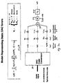
- FIGURE 1 is a simplified block diagram of a multibit sigma-delta analog-to digital converter 10 of a type generally known in the art, which includes correction of static nonlinearities introduced by a multibit DAC in the sigma-delta ( ⁇ ) feedback loop.
- the correction of FIGURE 1 results in significant reduction in passband DAC errors, given sigma-delta converters using low clock rates and narrow bandwidths (clock rates of about 5 MHz and bandwidths less than about 100 KHz at the current state of the art).
- Increased- or high-bandwidth sigma-delta converters use higher clock rates and wider bandwidths (clock rates of 500 MHz to 3.3 GHz, and bandwidths of 10 MHz to 100 MHz, at the present state of the art), and noise shaping bands centered at carriers such as 70 MHz to 1 GHz, at the present state of the art.
- the high-speed DACs used in such high-bandwidth sigma-delta loops will introduce error terms which result both from static and dynamic nonlinearities.
- the dynamic nonlinearities which account for mismatches in rise and fall times and overall delay skew between DAC levels differ from static nonlinearities, which account for only amplitude errors.
- the dynamic error is generally the dominant error term in high-speed multibit sigma-delta analog-to-digital converters. Therefore, multibit sigma-delta error correction capable of correction of dynamic nonlinearities would be advantageous.
- analog input signals applied to an analog input port 12 are summed in a summing circuit 14 with correction signals applied to an input port 142 from a signal path 24.
- the summed analog and correction signals are applied from summing circuit 14 to an input port 16i of a baseband multibit signal-delta modulator 16.
- Parallel sampled binary digital signals representing the analog input signals applied to input port 16i are produced at output port 16o.
- the digital signals at output port 16o are applied to the address input ports of a programmable ROM and to a static DC level calibrator 20.
- PROM 18 is preprogrammed at each memory location with error correction values established by the static DC level calibrator 20, for producing corrected signals y(n) at its output port 18o.
- Averaging circuit 20 receives the parallel sampled binary digital signals y(n) from output port 16o and averages or integrates the samples in an averager 22 by summation over a large number of samples, such as for example one thousand or more samples.
- the parenthetical expression (n) in the expression y(n) represents the index number of each of the samples.
- the averaging in block 20 removes quantization noise produced by the baseband multibit sigma-delta ( ⁇ - ⁇ ) modulator 16.
- level calibrator 20 which, at initial turn-on, or during a calibration procedure, produces a known direct level, such as a direct voltage or bias, which is applied over a signal path 24 to input port 14i of summing circuit 14, for addition or injection of the direct level for measuring direct (DC) offsets at the output of multibit sigma-delta modulator 16.
- the DC calibrator will inject a direct level corresponding to each of the multibit quantization levels.
- the averager provides measured offsets for each of these levels. These measured offsets are subtracted front the corresponding level values, to produce look-up table values which compensate for the offsets when applied to PROM 18.
- Static DC level calibrator 22 also produces signals which program the memory locations according to this table.
- PROM 18 removes error introduced into the passband of the sigma-delta modulator 16 produced by the multibit digital-to-analog converter inherent therein.
- FIGURE 1 the arrangement of FIGURE 1 is that of a known analog-to-digital converter. It should be noted that the PROM 18 and feedback calibrator 22 correct only baseband nonlinearity errors produced by static or constant gain mismatches inherent in the sigma-delta modulator, because averager 20 can only detect direct bias errors occurring at or near zero Hz.
- a sigma-delta modulator is illustrated within block 16.
- the particular sigma-delta modulator which is illustrated is the multibit ⁇ - ⁇ modulator with static error correction which is described in M. Nejad & G. Temes, "Multibit Oversampled Sigma-Delta A/D Converter with Digital Error Correction,” published at pp. 1051-1052 in Vol. 24 of IEEE Electronics Letters, June 1993.
- the arrangement of FIGURE 1 illustrates the Nejad et al. converter within block 16.
- analog-to-digital converter 16 includes a first summing circuit 30 which has a noninverting (+) input port 30 1 coupled to the output port of summing circuit 14, and an inverting (-) input port 30 2 coupled for receiving, from a feedback signal path 41b, feedback signal in the form of reconstructed analog signal.
- First summing circuit 30 subtracts the reconstructed analog signal from the analog input signal applied to input port 16i, to generate a ⁇ (t) signal.
- the ⁇ (t) signal is applied through an additional theoretical or hypothetical summing circuit 32 to an input port of an integrating loop filter 34.
- Hypothetical summing circuit 32 is considered to be the location at which equivalent input loop filter noise ⁇ (t) of the following circuits is added to the ⁇ (t) signal.
- Integrating loop filter 34 integrates the delta signal from hypothetical summing circuit 32, to produce integrated signals u(t) at its output port.
- the integrating loop filter 34 has poles place near zero Hz for producing frequency selective gain in the passband of the sigma-delta modulator, which is centered at zero Hz.
- the loop filter 34 is preferably an active filter.
- the filtered signals u(t) at the output port of filter 34 are applied to a multibit analog-to-digital converter illustrated as a block 36, which operates at the frequency f s of a clock signal applied over a signal path 37.
- Block 36 includes a further hypothetical noise source illustrated as a summing circuit 38, which adds to the digitized output signal a noise component which can be termed ADC quantization noise or equivalent error signals e(n), which includes quantization noise.
- ADC quantization noise or equivalent error signals e(n) which includes quantization noise.
- the digitized (discrete in both time and level) output signals from ADC 36 are applied as an output signal to output port 16o of sigma-delta modulator 16, and within sigma-delta modulator 16, are applied over a feedback signal path 41a of a feedback loop 39 to a digital-to-analog converter illustrated as a block 40.
- DAC 40 converts the digitized signal from the output port of ADC 36 into the reconstructed analog signal at the clock frequency f s , and applies the resulting converted signal over a signal path 41b of feedback loop 39 to the inverting input port 30 2 of summing circuit 30.
- DAC 40 also includes a further hypothetical summing circuit 42, which adds an equivalent error signal, produced by nonlinearity of the ADC 40, to the converted output signal.
- the ADC 36 and DAC 40 are often a part of a common integrated circuit.
- ADC 36 and DAC 40 may use specialized forms of coding, such as binary, thermometer, and level.
- the coupling between ADC 36 and output port 26o of multibit analog-to-digital converter 16 often includes a code converter, illustrated as 17, for converting the code used internally between ADC 36 and DAC 40 into ordinary digital code at output port 16o.
- sigma-delta modulator 16 processes noise over its passband produced by nonlinearity in the DAC 40, which, at the output of the ADC 36, tends to be larger than the shaped quantization noise characterized as the ADC quantization noise e(n), attenuated by the noise transfer function of the sigma-delta modulator over the passband.
- the nonlinearity noise g(t) is not attenuated by the sigma-delta loop, and so tends to limit the dynamic range of the ADC 16.
- PROM 18 and static dc level calibrator 22 are provided in the prior art to ameliorate the effect of the nonlinearities produced by DAC 40 by at least partial cancellation or reduction of noise.
- An analog-to-digital converter for converting analog input signals to parallel digital form, includes a multibit sigma-delta modulator including an input port to which the analog input signals are applied, and which produces an oversampled digital parallel data stream at its output port.
- the performance of the sigma-delta modulator is subject to errors caused by both dynamic and static nonlinearity.
- a nonlinear filter correction is coupled to the output port of the sigma-delta modulator, for receiving the parallel digital data stream.
- the nonlinear filter corrector in response to the parallel digital data stream, generates at least one of a real and imaginary component (that is to say, the real component, the imaginary component, or both) of an estimate of the errors, and for subtracting the one (or both) of the real and imaginary components of the estimate of the errors from equivalent components of the parallel digital data stream.
- This subtraction producing at least a real component of the parallel digital data stream, corrected for the nonlinearity.
- a filter with at least a low-pass characteristic is coupled to receive the one of the real and imaginary components of the parallel digital data stream, for removing out-of-band signal components therefrom.
- the filter with a low-pass characteristic is a decimation filter.
- the nonlinear filter corrector further generates the other one of the real and imaginary components, and subtracts both the real and imaginary components of the estimate of the error from equivalent components of the parallel digital data stream, for thereby generating, in addition to the real component, an imaginary component of the parallel digital data stream.
- the nonlinear filter corrector comprises a tapped delay line coupled to the parallel data stream, for generating a delayed sample of the parallel data stream at least one tap.
- a lockup table is coupled to the tap, for producing real and imaginary components of the estimated error of the delayed sample.
- a summing arrangement is coupled to the parallel digital data stream and to the lookup table, for subtracting the real and imaginary components of the estimated error from corresponding components of the parallel digital data stream.
- PROM 18 of FIGURE 1 is programmed with a table of values which provides a transfer function that inherently cancels the effect of the static mismatches produced by DAC 40.
- the values are obtained by calculation of estimated nonlinearity errors from a straight-line least-squares fit of the bias estimates produced by averager 20.
- the calculation of the errors by Nejad et al. is based on a priori knowledge of the dc level applied from the external signal source to input port 14 2 , which requires high linearity in the direct voltage generated by the static dc level calibrator 22 in order to avoid calibration errors.
- the corresponding value produced by the memory from the accessed location includes the input (address) value plus an error-correction value.
- the representation of the basic value plus the error-correction value requires more bits than would be required for representation of the basic value alone.
- Figure 5a is a simplified analytical representation of a portion of the arrangement of FIGURE 1, and more specifically of the code converter 17 (if used) and PROM 18, with PROM 18 preprogrammed by averager 20 and static DC level calibrator 22.
- the individual codes at the output of code converter 17 are designated c 1 (n), . . ., c i (n), . . ., c N .
- These codes c 1 (n), . . ., c i (n), . . ., c N are multiplied or weighted by idealized code weights W 1 , . .
- the multiplied output signals from set 512 of multipliers are summed together in a summing circuit or node illustrated as 516 of Figure 5a, and the summed signals are applied to a block 516, representing modulation of the output signals from summing nods 514 by an impulse function ⁇ n ⁇ (t-nTs).
- the modulated signals from block 516 are applied to a block 518, which is an output filter for signal reconstruction, which reconstructs the DAC output analog signal.
- the equation of FIGURE 6b represents the operation of the arrangement of Figure 6a.
- the arrangement of Figure 6a, implementing the equation of FIGURE 6b corrects static errors, but cannot correct dynamic errors.
- the equation for y r (t), which represents the analog output of DAC model of Figure 6a, includes the term W i , which represents a weight applied to a specific code sequence within the DAC structure.
- W i represents a weight applied to a specific code sequence within the DAC structure.
- Three possible candidates for value W i can be used, which are for binary, thermometer, and level code.
- the equations given for weight values are selected to correspond to the coding type selected within the DAC, which may be binary format in r-2r DACs, or thermometer in other types of DACs.
- Level code is provided in the equation in order to aid in modeling the thermometer code, but is not normally used within the actual DAC structure.
- Many DACs combine binary and thermometer coding in various arrangements (segmented DACs).
- the representation of Figure 5a models only static DAC errors from amplitude misalignments of the actual DAC codes represented within the model as ⁇ i .
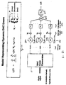
- analog input signals applied to an input port 212 are converted into digital signals by an analog-to-digital converter (DAC) arrangement 210.
- Analog-to-digital converter 210 includes a multibit sigma-delta modulator 216, which is very much like multibit sigma-delta modulator 16 of FIGURE 1 in form or topology, but which differs therefrom in a significant particular.
- analog input signals applied to input port 212 are coupled through a summing circuit 214 to the noninverting input port 230 1 of a summing circuit 230, where they are summed with reconstructed analog signals y(t) applied to an inverting input port 230 2 from a feedback path 239 including a DAC 240.
- the summed signals are applied to the input port 236i of an ADC 236 by way of a hypothetical summing circuit 232, corresponding to hypothetical summing circuit 32 of FIGURE 1.
- the signals from summing circuits 230 and 232 of FIGURE 2 are applied to a resonator 234.
- Resonator 234 may be of the type described in U.S. Patent 5,392,042, issued February 21, 1995 in the name of Pellon.
- the output signals u(t) from resonator loop filter 234 of FIGURE 2 are applied to a multibit analog-to-digital converter 236, corresponding to ADC 36 of FIGURE 1.
- Multibit ADC 236 (including code converter 217, if needed) converts the signals into multibit digital form y(n), and applies the signals so converted over a signal path 219 to an input port 250i of a nonlinear filter corrector designated generally as 250.
- the converted signals y(n) at the output of the multibit ADC 216 (and converter 217) are also applied, under certain conditions described below, over a signal path designated 219 1 to a dynamic error calibrator 280.
- Nonlinear filter corrector 250 of FIGURE 2 compensates for some of the nonlinearities generated in the sigma-delta analog-to-digital converter 216 of FIGURE 2.
- the nonlinearities which are corrected are those indicated as input g(t) which are effectively "injected” into the feedback path of multibit sigma-delta modulator 216, which feedback path includes signal path 241 and digital-to-analog converter 240.
- these errors are not reduced by the closed loop of the converter, but instead undesirably modulate the digital output signal of the analog-to-digital converter (ADC) 236.
- nonlinear filter corrector 250 includes a nonlinear filter error estimator 251.
- Nonlinear filter error estimator 251 includes a tapped delay line designated generally as 252, including M taps 254 separated by a corresponding number of delay elements 252a, 252b, . . ., each having delay designated by z -10 , z -11 ,. . ..
- Tapped delay line 252 generates delayed versions of the digital output signal applied over signal path 219 to nonlinear filter corrector 250 from ADC modulator 216.
- M may be viewed as equaling two, so there are two delays actually illustrated, designated 252a and 252b, each terminating at a tap. More particularly, delay 252a terminates at a tap 254a, and delay element 252b terminates at a tap 254b.
- the outputs of taps 254a, 254b, and any other of the M taps, are coupled to a set 256 of corresponding lookup tables or addressable ROMs T1, T2, . . ., which are preprogrammed in a manner described below, to produce real and imaginary (or possibly I and Q) components, or possibly only real components, of an estimate of the noise signal g(t).
- set 256 includes memory locations which, in general, are preprogrammed with real and imaginary components signals.
- the real and imaginary signals from the lookup tables are separately summed in a summing circuit illustrated as 258, to produce real components of an estimate of the noise signal g(t).
- the summed signals produced by summing circuit 258 represent the output signal of nonlinear filter error estimator 251.
- the summed signals produced by summing circuit 258 of nonlinear filter error estimator 251 are applied to an inverting (-) input port of a further summing circuit 260,
- the summed signals generated in summing circuit 258 of nonlinear filter error estimator 251, which represent the real and imaginary components of an estimate of the nonlinearity or error signals g(t) are applied to an inverting (-) input port of summing circuit 260, and are subtracted therein from corresponding components of the digital output signal of the sigma-delta modulator.
- This subtraction of the real and imaginary components of the estimated error signal g(t) reduces the error component of the output digital signal y(n) at output port 250o of nonlinear filter corrector 250.
- a decimating filter 270 is coupled to output port 250o to receive the output signals from nonlinear filter corrector 250, to eliminate out-of-band signal components.
- the first delay element 252a of the tapped delay line 252 of the nonlinear filter corrector 250 of FIGURE 2 preferably has a delay which is an approximation of the delay between (a) the point of injection of noise signal g(t) into the feedback signal path 239 of sigma-delta modulator 216 and (b) the output port 216o of the sigma-delta modulator 216.
- the feedback path 239 of sigma-delta modulator 216 includes path 241b, digital-to-analog converter 240, and noninverting input port 230 2 , and the delay path also includes summing circuit 230, resonator 234, and sigma-delta ADC 236.
- the dynamic error calibrator 280 includes a low-noise oscillator 282, and a processor, logic state analyzer 284LSA, and bandpaas filter 284BPF, illustrated together as a block 284.
- processor block 284 controls oscillator 282 during calibration, to cause oscillator 282 to produce a single carrier on one of the edges of the passband of the multibit sigma-delta modulator 216, as established by the resonator loop filter 234, or two carriers, one on each of the upper and lower edges of the passband.
- the oscillator signals are applied over a signal path 224 to input port 214 2 of summing circuit 214, for injecting the oscillator signal into the signal flowing to the sigma-delta modulator 216.
- Multibit sigma-delta modulator 216 processes the calibration signals, and produces processed calibration signals at its output port 216o.
- Processed calibration signals in the form of multibit digital signals applied over signal path 219 1 to first input port 284 i1 of processor block 284, in conjunction with lag constants L 0 , L 1 , L 2 , . . . , applied to input port 284 i2 .
- Processor block 284 receives the multibit digital signal at its input port 284 i1 and the lag constants at its input port 284 i2 , and processes the data, to determine the values or weights which should program the various memory locations of look-up tables T1, T2, . . . of set 256 of look-up tables. It should be noted that the invention is not limited to particular delays of the delay elements T1, T2, . . ., but that improved performance is achieved over a wide range of delay values.
- FIGURES 3a, 3b, 3c, 3d, and 3e represents the steps performed during calibration of the system of FIGURE 2 by use of the dynamic error calibrator 280 of FIGURE 2.
- the process represented by FIGURES 3a, 3b, 3c, 3d, and 3e includes process steps performed as operator inputs to the process, and also include automatic calculations performed by a processor. Put another way, the process is intended to be performed by an electronic processor, but certain operator inputs arm needed before the processing can be performed.
- the calibration process generally described above need not be performed continuously, but rather can be performed in the factory at the time the ADC is fabricated, or possibly at initial start-up in a particular application, or occasionally during use.
- recalibration should occur whenever the tuning of the loop filter 234 is changed, to choose different bandwidth or center frequency. It might also be desirable to recalibrate (or use pre-generated calibrations) at different operating temperatures of the ADC 210, to compensate for differences in errors which are attributable to the temperature of the active elements.
- both real and imaginary components are used in order to achieve improved estimates of phase components of the nonlinearity, but real-only may be used in conjunction with simplified downstream processing, with adequate results.
- downconverters and decimation filters are used in the downstream processing.
- the downconversion for the case in which both real and imaginary components are used requires complex multiplication. When only real components are used, real multiplication can be used, thereby simplifying the down-converter. It downconversion is not used, the decimation filter may similarly be simplified when only real components are used.
- the order of nonlinear filter corrector 250 of FIGURE 2 is typically twice that of the case using both real and imaginary components.
- order means the number of taps and their corresponding tables; in the case illustrated in FIGURE 2, the order is two, because there are only two delay-element/look-up table pairs, namely pair 252a/T1 and 252b/T2.
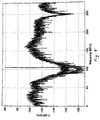
- FIGURE 4 illustrates two overlapping plots, which coincide over most of the illustrated frequency range, except in the range of about 95 to 105 Mhz.
- the lowermost or lower-amplitude of the plots of FIGURE 4 represents the quantization noise over a range including the bandpass of the sigma-delta modulator 216 of FIGURE 2.
- the lowermost plot of FIGURE 4 which is a plot of quantization noise, has a region about 100 MHz. In the lowermost plot of quantization noise, the region around 100 MHz is affected by the resonator, which reduces the loop quantization noise to below -180 dB below full-scale/Hz, where full scale represents half the peak amplitude allowed by the converter from its center value.
- the upper plot of FIGURE 4 which coincides with the lower plot except in the resonator notch around 100 MHz, represents the noise attributable to dynamic nonlinearity of DAC 244 of FIGURE 2.
- the DAC nonlinearities were simulated in a computer.
- the DAC error model used in the simulation included DAC cell reconstruction filters with mismatches in both group delay and amplitude, thereby representing dynamic error.
- the CW error excitation signal is represented by a peak at a frequency of about 80 MHz.
- the amplitudes of the error excitation signal(s) are selected to exercise or excite all the codes which represent levels out of the sigma-delta modulator 216; this requires a full-scale calibration signal; there must also be some offset between the frequency of the error excitation frequency which is nonsynchronous with the system clock frequency. Also, the error excitation signal must not itself introduce excessive noise within the passband; this can be guaranteed by use of a source with low phase noise, or by the use of an additional passband filter (not illustrated) at the output of generator 282 of FIGURE 2.
- FIGURE 6a is a simplified conceptual representation of the combination of static and dynamic DAC errors in the structure of FIGURE 2, implementing the equation set forth in FIGURE 6b. This is a more thorough model than Figure 5a and the equation of FIGURE 5b.
- the DAC code (at the output of code conversion block 17, if used) is designated c 1 (n), . . ., c i (n), . . ., c N , as in Figure 6a.
- the DAC codes are individually modulated in a set 616 of modulator blocks 616 a , .
- Each modulated, weighted, individual code is filtered by a set of mismatch or code reconstruction filters, designated together as 620, each having impulse response given by . . ., . . ., respectively.
- the mismatches may be represented as changes in gain, delay, phase, andor spectral response. These mismatches represent total error, including both static and dynamic error.
- the modulated, weighted, and filtered individual codes are summed at a summing node 614 of FIGURE 6a, to produce the desired analog reconstructed signal y r (t) including static and dynamic errors.
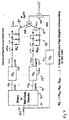
- FIGURE 7 is a simplified conceptual block diagram representing the processing which is performed in dynamic error calibrator 280 of FIGURE 2 in order to determine the coefficients for the look-up tables of set 256.
- the converted code y(n) produced at the output port 236 of FIGURE 2 is applied over a signal path 710 to a digital filter 712 and to a binary-to-DAC-code converter 714.
- Digital filter 712 has characteristic H D , which is a low-pass or bandpass characteristic, for passing the DAC error within the band of interest, and for attenuating components outside the band of interest.
- Code converter 714 performs the reverse of the code transformation performed by code converter 217 of FIGURE 2, to produce a plurality of codes c 1 (n), . .
- each individual code on a signal path of set 716 is filtered by a corresponding filter 718 1 , . . ., 718 Nt of a set 718 of filters, each having filter characteristic H D .
- the output weight of each H D filter 718 1 , . . ., 718 Nt of set 718 is a bandlimited code signal C di (n), which is applied over a signal path 720 1 of a set 720 of signal paths to a set 722 of transversal filters 722 1 , . . ., 722 Nt .
- Nt includes delays variously designated as z -L0 , z -L1 , z -L2 , . . ., where z -1 represents an incremental delay equal to one clock interval and where the values L 0 , L 1 , L 2 , . . . are the delays of the delay elements of set 252 of FIGURE 2.
- the delays are selected to correspond to the delays used in the nonlinear filters of set 252 of filters of FIGURE 2.
- first index i represents the signal paths corresponding to 720
- the second index which progresses from 0 to M-1, represents the weights applied to tapped signals from the tapped delay line.
- the filtered outputs y g1 through y gnt from the plurality of transversal filters of set 722 are applied to a summing circuit or node 758, in which they are summed together to generate a representation or estimate of the errors y gd (n) in the output of multibit ⁇ modulator 216 of FIGURE 2.
- Each of these signals represents estimates of errors contributed by each code sequence to the total error y gd (n).
- the estimated errors y gd (n) generated at the output of summing node 758 are applied to the inverting (-) input port of summing circuit 760, to produce the corrected multibit digital signal e representative of the analog signal applied to input port 212 of FIGURE 2.
- the selection of the weights may be obtained by a least-squares solution, described in conjunction with the flow chart of FIGURES 3a, 3b, 3c, 3d, and 3e.
- the process or logic starts at a block 310, which represents obtainance of certain properties of the multibit sigma-delta modulator 216 of FIGURE 2, namely the center frequency of the passband, the bandwidth, and the notch depth provided by the resonator 234 acting within the feedback loop of the sigma-delta modulator 216.
- This information can be obtained by measurements performed on a hardware apparatus or by the setting of coefficients in a software embodiment.
- block 312 represents the setting of coefficients within digital software-implemented bandlimiting filter 284BPF of processor 284 of FIGURE 2, so that only the error components of the output signal of sigma-delta modulator 216, flowing over signal path 219 1 to the processor 284, are stored within memories (logic state analyzer 284LSA) associated with the processor for further use.
- a logic state analyzer may be used in association with processor 284 for synchronously capturing the samples, and for storing them in memory for later use by processor 284.
- block 312 represents selection of h D (n), which are finite impulse response (FIR) values, as the coefficients of the bandlimiting filter 284BPF within processor 284.
- the digital filter may also be implemented as an IIR filter, but this is not the preferred form of the filter. Selection of these coefficients produces a spectral response H D (e jwn ) which coincides with the passband of the multibit sigma-delta modulator 216.
- the stop-band response of bandlimiting filter 284BPF is selected to attenuate the quantization noise at the output of sigma-delta modulator 216 to a level which makes the quantization noise negligible relative to the noise components within the passband, and to attenuate the error excitation signals (those generated by oscillator 282 of FIGURE 1) at selected frequencies outside the passband (the continuous-wave or CW calibration signals lie in notches in the filter response).
- the order of bandlimiting filter 284BPF may typically range from 100 to 600.
- the logic flows to a further block 314, which represents energization of the oscillator(s) 282 of FIGURE 2 to produce the CW error excitation signal, which is applied over signal path 224 to input port 214 2 , and which flows through the multibit sigma-delta modulator 216 to output port 216o, and back to the dynamic error calibrator 280 by way of signal path 219 1 .
- the error excitation signals are selected to be just outside the passband of the band limiting filter, each in its own notch.
- the logic flows to a block 316, which represents collection of real-time responses by the logic state analyzer portion 284LSA of calibrator 280 of FIGURE 2, i.e. the catching and storing of the output signals from sigma-delta modulator 216.
- the data so collected for later use is designated y(n).
- the logic flows by way of a logic node A to a further block 320.
- the type of DAC coding is selected in a block 318 prior to further operations; the type of coding is a known parameter of the processing in sigma-delta modulator 216. Included within the possible types of coding are binary codes and thermometer codes.
- Block 320 of FIGURES 3a, 3b, 3c, 3d, and 3e represents a portion of the processing performed in processor block 284 of FIGURE 2. More particularly, block 320 of FIGURES 3a, 3b, 3c, 3d, and 3e represents the conversion of the data collected in block 316 into parallel digital DAC code signals, arranged as a matrix C, which is set forth in block 320. Matrix C represents the code of samples y(n) (on signal path 219 1 of FIGURE 2), converted into a code corresponding to the code which DAC 240 of FIGURE 2 receives over signal path 241a to produce reconstructed analog signals on signal path 241b.
- matrix C represents the output of code conversion block 217 of FIGURE 2, "back-converted” into the original coding state at the input port of code conversion block 217.
- this original coding state may be binary, thermometer, or possibly some other type of code.
- the multibit sigma-delta modulator 216 of FIGURE 1 produces ordinary binary code at its output port 216o; if DAC 240 also uses ordinary binary cods, no actual code converter 217 is required in FIGURE 2, and no code conversion is required in block 320 of FIGURES 3a, 3b, 3c, 3d, and 3e, because the converted code is the same as the incoming code.
- the DAC coding will be thermometer coding. Such thermometer coding can be directly coupled to DAC 240 from comparators (not illustrated) within ADC 236.
- the numeric subscripts represent the particular stream of data which the sample represents in the back-converted code (that is, in the thermometer or other code flowing between ADC 236 and DAC 240), and the numeral in parentheses represents the time at which the sample occurs.
- the rows of the matrix C represent one of the parallel streams of converted data, which is to say, if there are N parallel streams of data in the multibit input signal applied to DAC 240 of FIGURE 2, each row of matrix C represents samples from a single such stream, and there must be N rows in matrix C.
- each element of matrix C of FIGURES 3a, 3b, 3c, 3d, and 3e is a single digit, which may take on values of zero (0) or one (1).
- Matrix C represents the stimulus into each of the cells (not separately illustrated) within DAC 240 of FIGURE 2, in the presence of the CW excitation signal.
- a block 322 which represents the step of filtering the signals of the set of DAC codes represented by matrix C with the bandlimiting filter 284BPF associated with dynamic error calibrator 280 of FIGURE 2. More particularly, the DAC codes represented by matrix C of block 320 are filtered by function h D (n). The result of this filtration is the production of bandlimited code signals c di (n), which can be represented by matrix C d , which matrix is set forth in block 322 of FIGURES 3a, 3b, 3c, 3d, and 3e.
- Each of the elements of matrix C d is identified by a subscript numeral and a parenthetical suffix, having the same meanings ascribed to the subscripts and suffixes of matrix C.
- the signals represented by matrix C d are the individual spectral contributions of each code sequence produced by DAC 240 and contributed to the band of interest, which is the passband of the bandlimiting filter 284BPF. While the unfiltered codes take on values of only one and zero, the filtered codes can take on values other than zero and one.
- the noise shaping of the sigma-delta modulator produces a correlation between the filtered code sequences represented in matrix C d such that the sum of these code sequences produces a signal sequence smaller, and preferably much smaller, in power than each individual code sequence; in other words, the summation of a plurality of code sequences, each having a standard deviation of 0.1, for example, may have the result of producing a summed signal with a standard deviation of 0.001.
- the logic flows by way of a logic node B to a block 324, which represents creation of an observation matrix X 0 .
- the logic of block 324 of FIGURES 3a, 3b, 3c, 3d, and 3e requires the information relating to the number of taps M and the magnitudes of the delays in the tapped delay line 252 of FIGURE 2, as set forth in block 326; this information must be provided before the operation of block 324 of FIGURES 3a, 3b, 3c, 3d, and 3e can begin.
- Observation matrix X 0 produced in block 324 organizes the available data from matrix C d for solution to determine the required look-up table values which are required in tables T1, T2, . . . of set 256 of look-up tables of nonlinear filter error estimator 251 of nonlinear filter corrector 250 of FIGURE 2.
- Matrix X 0 includes N T submatrices, corresponding to the number of codes N T in the backconverted data C d . Each sub-matrix has (vertical) height equal to the number of samples N s , and (horizontal) width equal to the number of taps M in the delay line 252 of FIGURE 2.
- matrix X 0 of block 324 Only the first, second, and last submatrices of matrix X 0 are illustrated in block 324 of FIGURES 3a, 3b, 3c, 3d, and 3e.
- matrix X 0 of block 324 the subscript portion of each element of each submatrix has the same meaning as in matrix C d , and the parenthetical suffixes, such as "(L 0 +1)", represent the transformed locations of the elements.
- the data in the observation matrix is arranged in a regular pattern in which each code will have multiple adjacent columns of data within X 0 , with each column representing a set of samples in time of each converted code, with lag corresponding to one selected lag or delay.
- the lags (L x ) represent the delays of the delay elements 252x of FIGURE 2.
- matrix X 0 of block 324 of FIGURES 3a, 3b, 3c, 3d, and 3e consists of a plurality of sub-matrices, arrayed or set horizontally, of which only the first, second, and last sub-matrices are illustrated.
- Each sub-matrix of matrix X represents the data of one of the plurality of codes appearing on signal path 219 of FIGURE 2.
- the first or left-most sub-matrix includes a plurality of columns of data, arrayed horizontally.
- a column of data of matrix X 0 represents a particular lag provided by the delay elements 252 of FIGURE 2, and for each lag, there is a corresponding column of data.
- the left-most column of data of the first sub-matrix of matrix X 0 includes a vertical array of elements, ranging from the first element C d1 (L 0 ) at the top of the column to the last element C d1 (L 0 + N s ) at the bottom; only the first, second, and last elements of the first column are illustrated.
- the first element C d1 (L 0 ) represents the earliest sample of the first filtered code (code 1), delayed by the first delay element (252a of FIGURE 2), the second element from the top, C d1 (L 0 + 1) represents the next succeeding sample of filtered code 1, also delayed by first delay element 252a.
- the remainder of the first column of the left-most submatrix of matrix X 0 of FIGURES 3a, 3b, 3c, 3d, and 3e represents all the later samples of code 1 delayed by first delay element 252a, until the last or N th sample C d1 (L 0 + N s ), which appears at the bottom of the first column of the first sub-matrix.
- the next or second column of the first sub-matrix (not illustrated), represents the same code 1, delayed by the sum of the delay of the next delay element and all previous accumulated delays, which in the case of column 2 represents the summation of the delays of both first and second delay elements 252a and 252b of FIGURE 2.
- the last or right-most column in the first or left-most sub-matrix of matrix X 0 represents the same code 1, delayed by the summation of all the delays 252, including the last or (M-1) th of the delay elements of FIGURE 2.
- the left-most column of data of the second sub-matrix of matrix X 0 (the second sub-matrix from the left) of block 324 of FIGURES 3a, 3b, 3c, 3d, and 3e includes a vertical array of elements, ranging from the first element C d2 (L 0 ) at the top of the column to the last element C d2 (L 0 + N s ) at the bottom; only the first, second, and last elements of the first column of the second sub-matrix are illustrated.
- the first element C d2 (L 0 ) represents the earliest sample of the second filtered code (code 2), delayed by the first delay element 252a, the second element from the top, C d2 (L 0 + 1) represents the next succeeding sample of filtered code 2, also delayed by first delay element 252a.
- the remainder of the first column represents all the later samples of code 2 delayed by first delay element 252a, until the last or N th sample C d2 (L 0 + N s ), which appears at the bottom of the first column of the second sub-matrix.
- the next or second column of the second sub-matrix (not illustrated), represents the same code 2, delayed by the sum of the delay of the next delay element and all previous accumulated delays, which in the case of column 2 represents the summation of the delays of both first and second delay elements 252a and 252b of FIGURE 2.
- the last or right-most column in the second sub-matrix of matrix X 0 represents the same code 2, delayed by the summation of all the delays 252, including the last or (M-1) th of the delay elements of FIGURE 2.
- the left-most column of data of the last or N th sub-matrix of matrix X 0 (the last sub-matrix from the left, or the right-most submatrix) of block 324 of FIGURES 3a, 3b, 3c, 3d, and 3e includes a vertical array of elements, ranging from the first element C DNT (L 0 ) at the top of the column to the last element C DNT (L 0 + N s ) at the bottom; only the first, second, and last elements of the first column of the last sub-matrix are illustrated.
- the first element C DNT (L 0 ) represents the earliest sample of the N th filtered code (code N T ), delayed by the first delay element 252a, the second element from the top, C DNT (L 0 + 1) represents the next succeeding sample of filtered code N T , also delayed by first delay element 252a.
- the remainder of the first column represents all the later samples of code N T delayed by first delay element 252a, until the last or N th sample C DNT (L 0 + N s ), which appears at the bottom of the first column of the last sub-matrix.
- the next or second column of the last sub-matrix (not illustrated), represents the same code N T , delayed by the sum of the delay of the next delay element and all previous accumulated delays, which in the case of column 2 represents the summation of the delays of both first and second delay elements 252a and 252b of FIGURE 2.
- the last or right-most column in the last sub-matrix of matrix X 0 represents the same code N T , delayed by the summation of all the delays 252, including the last or (M-1) th of the delay elements of FIGURE 2.
- the logic of the calibration flows, by way of a logic node C, to a block 328, which represents conditioning of the observation matrix X 0 with noise, to assure numerical stability (to eliminate non-convergence of the mathematical processing).
- the conditioning with noise is also required to constrain the solution to small table values. This constraint eliminates the possibility of producing a nonlinear filter that cancels the desired signal.
- the conditioning is accomplished by addition of noise to the elements of the observation matrix X 0 in the following manner.
- a preferred method of introducing noise is to multiply the observation matrix X 0 by a similarly dimensioned matrix in which each element is made up of the value unity plus a scaled random variable.
- Block 330 represents calculation of the covariance matrix R and the desired-signal vector .
- the covariance matrix R (X 0 H )(X 0 ) , where X 0 H is the complex conjugate transpose of X 0 .
- the desired-signal vector [d(1), d(2),.. .,d(N s )], where the square bracket denote, a vector, and the desired signal represents the DAC error over the passband of the bandlimiting filter 284BPF.
- the elements of vector are given by
- the logic of the calibration flows to a block 332, which solves for the error filter weights.
- the solution is performed as a standard Weiner solution as set forth in block 332.
- the first step in the processing of block 332 is to create vector P by multiplication of vector with the complex conjugate of matrix X 0 .
- Vector P represents the cross-correlation between the desired signal vector and the observations represented by X 0 .
- the vector W e is calculated as the product of the inverse of covariance matrix R and matrix P.
- the vector W e will have elements comprising the coefficients of the error filter, and arranged in sets corresponding to each code index.
- the first set of coefficients ranging from W e0 to W e1M-1 will correspond to the error filter coefficients of code 1 for each of the accumulated delays, which in turn correspond to each of the look-up tables.
- a second set of elements W e20 to W e2M-1 similarly corresponding to the error filter coefficients for code 2 for each of the accumulated delays, is concatenated with the first set of elements.
- each of the elements of vector W e corresponds to the coefficients for one of the look-up tables T1, T2 of set 256.
- Blocks 336, 338, and 340 of FIGURES 3a, 3b, 3c, 3d, and 3e represent the generation of the look-up table values T ekm by various equations, which are set out in the blocks. From any one of blocks 336, 338, or 340, the logic flows to a block 342, which represents application of the table look-up values T ekm to the appropriate memory locations k,m in the look-up tables of set 256 of FIGURE 2, where k,m is the location addressed by signal amplitude value k within that look-up table associated with tap delay number m.
- the equations in the boxes provide translation of the values in vector W e to values in the table T ekm .
- FIGURE 8 includes two superposed plots as in FIGURE 4 showing the resulting output y c (n) produced by the ADC 210 of FIGURE 2 including nonlinear filter correction for both static and dynamic errors as described above.
- the signal applied to the converter is represented by the sharp peak or spectral line within the passband of the sigma-delta modulator, and this spectral line appears on both the upper and the lower plots within the passband of 95 to 105 MHz.
- the upper plot represents the uncorrected signal y(n) generated at output port 219 of the multibit sigma-delta modulator 216 of FIGURE 2
- the lower plot represents the corrected output signal y c (n) at output port 250 o of nonlinear filter corrector 250 of FIGURE 2.
- the corrector according to the invention improves the dynamic range by about 20 dB.
- look-up tables T1 and T2 of set 256 have been described as being ROMs, they are read-only in the context of normal (non-calibration) operation; the look-up tables are preferably controllable memories such as RAM, so that the calibration procedure can be readily invoked at initial turn-on or at any other time.
- Various portions of the arrangement of FIGURE 2 may be in the form of hardware, firmware, or software.
- an analog-to-digital converter (210) for converting analog input signals to parallel digital form, includes a multibit sigma-delta modulator (16; 216) including an input port (16i; 216i) to which the analog input signals are applied, and which produces an oversampled digital parallel data stream at its output port (16o; 216o).
- the performance of the sigma-delta modulator (16; 216) is subject to errors caused by both dynamic and static nonlinearity.
- a nonlinear filter corrector (250) is coupled to the output port (16o, 216o) of the sigma-delta modulator (16, 216), for receiving the parallel digital data stream.
- the nonlinear filter corrector (250) in response to the parallel digital data stream, generates at least one of a real and imaginary component (that is to say, the real component, the imaginary component, or both) of an estimate of the errors, and for subtracting the one (or both) of the real and imaginary components of the estimate of the errors from equivalent components of the parallel digital data stream. This subtraction produces at least a real component of the parallel digital data stream, corrected for the nonlinearity.
- a filter (270) with at least a low-pass characteristic is coupled to receive the one of the real and imaginary components of the parallel digital data stream, for removing out-of-band signal components therefrom.
- the filter (270) with a low-pass characteristic is a decimation filter.
- the nonlinear filter corrector (250) further generates the other one of the real and imaginary components, and subtracts both the real and imaginary components of the estimate of the error from equivalent components of the parallel digital data stream, for thereby generating, in addition to the real component, an imaginary component of the parallel digital data stream.
- the nonlinear filter corrector (250) comprises a tapped delay line (252) coupled to the parallel data stream (on signal path 219), for generating a delayed sample of the parallel data stream at at least one tap (254a).
- a lookup table (T1 of set 256) is coupled to the tap (254a), for producing real and imaginary components of the estimated error of the delayed sample.
- a summing arrangement (258, 260) is coupled to the parallel digital data stream and to the lookup table, for subtracting the real and imaginary components of the estimated error from corresponding components of the parallel digital data stream.
Abstract
Description
Claims (7)
- An analog-to-digital converter for converting analog input signals to parallel digital form, said analog-to-digital converter comprising:a multibit sigma-delta modulator including an input port to which said analog input signals are applied, and which produces an oversampled digital parallel data stream at its output port, the performance of said sigma-delta modulator being subject to errors caused by both dynamic and static nonlinearity;nonlinear filter correction means coupled to said output port of said sigma-delta modulator for receiving said parallel digital data stream, for generating one of a real and imaginary component of an estimate of said error, and for subtracting said one of said real and imaginary components of said estimate of said error from equivalent components of said parallel digital data stream, for thereby producing at least a real component of said parallel digital data stream, corrected for said nonlinearity; anda filter with at least a low-pass characteristic, said filter being coupled to receive said one of the real and imaginary components of said parallel digital data stream, for removing out-of-band signal components therefrom.
- An analog-to-digital converter according to claim 1, wherein said nonlinear filter correction means further generates the other one of said real and imaginary components, and subtracts both said real and imaginary components of said estimate of said error from equivalent components of said parallel digital data stream, for thereby generating an imaginary component of said parallel digital data stream in addition to said real component.
- A converter according to claim 1, wherein said nonlinear filter correction means comprises:a tapped delay line coupled to said parallel data stream, for generating a delayed sample of said parallel data stream at at least one tap:a lookup table coupled to said tap, for producing real and imaginary components of the estimated error of said delayed sample; andsumming means coupled to said parallel digital data stream and to said lookup table, for subtracting said real and imaginary components of said estimated error from corresponding components of said parallel digital data stream.
- An analog-to-digital converter for converting analog input signals to parallel digital form, said analog-to-digital converter comprising:a multibit sigma-delta modulator including an input port to which said analog input signals are applied, and which produces an oversampled digital parallel data stream at its output port, the performance of said multibit sigma-delta modulator being subject to errors caused by both dynamic and static nonlinearity;nonlinear filter correction means coupled to said output port of said sigma-delta modulator for receiving said parallel digital data stream, for generating I and Q components of an estimate of said error, and for subtracting said I and Q components of said estimate of said error from equivalent components of said parallel digital data stream, for thereby producing I and Q components of said parallel digital data stream corrected for said nonlinearity; anda filter with at least a low-pass characteristic coupled to receive said I and Q components of said parallel digital data stream, for removing out-of-band signal components therefrom.
- A converter according to claim 4, wherein said correction means comprises:a tapped delay line coupled to said parallel data stream, for generating at one delayed sample of said parallel data stream at at least one tap:a lookup table coupled to said tap, for producing real and imaginary components of the estimated error of said delayed sample; andsumming means coupled to said parallel digital data stream and to said lookup table, for subtracting said real and imaginary components of said estimated error from corresponding components of said parallel digital data stream.
- A method for operating an analog-to-digital converter including(a) a multibit sigma-delta modulator including an input port to which said analog input signals are applied, and which produces an oversampled digital parallel data stream at its output port, the performance of said modulator being subject to errors caused by both dynamic and static nonlinearity, and(b) nonlinear filter correction means coupled to said output port for receiving said parallel digital data stream, for estimating said error, and for subtracting said estimated error from said parallel digital data stream, for thereby improving the dynamic range of said sigma-delta modulator, said method comprising the steps of:applying to said analog input port an sinusoidal analog training signal which is outside of the band of interest, and which is of an amplitude selected to exercise the full dynamic range of said sigma-delta modulator;storing in memory a set of sequential samples of said digital signal;using a model of the errors in said sigma-delta modulator, performing mathematical operations which define the delays and amplitude transfer functions of said nonlinear filter correction means, for tending to reduce said error.
- An analog-to-digital converter for converting analog input signals to parallel digital form, said analog-to-digital converter comprising:a sigma-delta modulator including an input port to which said analog input signals are applied, and also including a forward signal path for resonating, sampling and quantizing a difference signal for producing a parallel digital data stream which represents the analog input signal, and also including a feedback signal path for generating an analog reconstruction of said digital parallel output, for aiding in generating said difference signals, said analog reconstruction being subject to nonlinearities which are equivalent to an error signal added to said analog reconstruction, said error signal being encoded with a delay by said sigma-delta modulator;a summing circuit including a noninverting input port coupled to the output of said forward signal path, and also including an inverting input port, for subtracting an error signal from said parallel digital data stream; andnonlinear filter correction means coupled to maid output port of said forward signal path, for receiving said parallel digital data stream and said encoded, delayed error signal, said filter correction means comprising (a) a tapped delay line, including at least one tap, coupled to said output of said forward signal path.
Applications Claiming Priority (2)
| Application Number | Priority Date | Filing Date | Title |
|---|---|---|---|
| US8871198P | 1998-06-10 | 1998-06-10 | |
| US88711P | 1998-06-10 |
Publications (3)
| Publication Number | Publication Date |
|---|---|
| EP0964524A2 true EP0964524A2 (en) | 1999-12-15 |
| EP0964524A3 EP0964524A3 (en) | 2003-10-01 |
| EP0964524B1 EP0964524B1 (en) | 2006-03-22 |
Family
ID=22212988
Family Applications (1)
| Application Number | Title | Priority Date | Filing Date |
|---|---|---|---|
| EP99111345A Expired - Lifetime EP0964524B1 (en) | 1998-06-10 | 1999-06-10 | Nonlinear filter correction of multibit sigma delta modulators |
Country Status (6)
| Country | Link |
|---|---|
| US (1) | US6271781B1 (en) |
| EP (1) | EP0964524B1 (en) |
| JP (1) | JP2000224042A (en) |
| AU (1) | AU3397399A (en) |
| DE (1) | DE69930442T2 (en) |
| ES (1) | ES2258827T3 (en) |
Cited By (8)
| Publication number | Priority date | Publication date | Assignee | Title |
|---|---|---|---|---|
| FR2805940A1 (en) * | 2000-03-01 | 2001-09-07 | France Telecom | System for correcting digital-analogue converter for delta-signals modulator, for high resolution conversion |
| EP1639710A1 (en) * | 2003-06-27 | 2006-03-29 | Optichron, Inc. | Analog to digital converter |
| GB2430565A (en) * | 2005-09-23 | 2007-03-28 | Realtek Semiconductor Corp | Self-calibrating continuous time delta sigma modulator |
| US7277032B2 (en) | 2005-10-21 | 2007-10-02 | Realtek Semiconductor Corp. | Low-pass filter based delta-sigma modulator |
| US7321325B2 (en) | 2005-07-07 | 2008-01-22 | Realtek Semiconductor Corp. | Background calibration of continuous-time delta-sigma modulator |
| US7446687B2 (en) | 2006-10-27 | 2008-11-04 | Realtek Semiconductor Corp. | Method and apparatus to reduce internal circuit errors in a multi-bit delta-sigma modulator |
| GB2453255A (en) * | 2007-09-28 | 2009-04-01 | Intel Corp | A sigma-delta analog-to-digital converter (ADC) which has an integral calibration system comprising calibration digital-to-analog converters (DACs). |
| WO2018204001A1 (en) * | 2017-05-01 | 2018-11-08 | Teradyne, Inc. | Calibrating non-linear data |
Families Citing this family (54)
| Publication number | Priority date | Publication date | Assignee | Title |
|---|---|---|---|---|
| US7076228B1 (en) * | 1999-11-10 | 2006-07-11 | Rilling Kenneth F | Interference reduction for multiple signals |
| US6449569B1 (en) * | 1998-12-11 | 2002-09-10 | Cirrus Logic, Inc. | Calibration and compensation of delta sigma ADC's and DAC's by correlating noise signals |
| US6583741B1 (en) * | 1999-07-12 | 2003-06-24 | National Instruments Corporation | System and method for self-calibrating a multi-bit delta-sigma analog to digital (A/D) converter during operation of the A/D converter |
| US6639537B1 (en) * | 2000-03-31 | 2003-10-28 | Massachusetts Institute Of Technology | Highly linear analog-to-digital conversion system and method thereof |
| US6404369B1 (en) * | 2000-09-29 | 2002-06-11 | Teradyne, Inc. | Digital to analog converter employing sigma-delta loop and feedback DAC model |
| FR2823619B1 (en) * | 2001-04-11 | 2003-06-27 | Commissariat Energie Atomique | SIGMA-DELTA BANDWAY MODULATOR AND USES OF THE SIGMA DELTA MOLOR FOR CONVERSION, DETECTION AND PRODUCTION OF SIGNALS |
| US6768435B2 (en) * | 2001-11-13 | 2004-07-27 | National University Of Singapore | Bandpass sigma-delta modulator |
| US6587062B1 (en) * | 2001-12-27 | 2003-07-01 | Texas Instruments Incorporated | Flexible interface circuit and method for delta sigma A/D converters |
| EP1324497B1 (en) * | 2001-12-27 | 2004-09-29 | STMicroelectronics S.r.l. | Method for self-calibrating a frequency of a modulator circuit, and circuit using said method |
| SE523353C2 (en) * | 2002-04-26 | 2004-04-13 | Ericsson Telefon Ab L M | Digital / Analog converter with error compensation |
| US6946983B2 (en) * | 2002-04-26 | 2005-09-20 | Telefonaktiebolaget L M Ericcson | Digital-to-analog converter having error correction |
| US7065166B2 (en) * | 2002-12-19 | 2006-06-20 | Texas Instruments Incorporated | Wireless receiver and method for determining a representation of noise level of a signal |
| US6961385B2 (en) * | 2003-01-21 | 2005-11-01 | Cirrus Logic, Inc. | Signal processing system with baseband noise modulation chopper circuit timing to reduce noise |
| US6861968B2 (en) * | 2003-01-21 | 2005-03-01 | Cirrus Logic, Inc. | Signal processing system with baseband noise modulation and noise filtering |
| DE10305972A1 (en) * | 2003-02-13 | 2004-09-02 | Micronas Gmbh | Compensation circuitry and compensation method for compensating for non-linear distortion of an AD converter |
| US6907374B1 (en) | 2003-03-19 | 2005-06-14 | Zilog, Inc. | Self-calibrating sigma-delta analog-to-digital converter |
| US7894536B2 (en) * | 2003-04-15 | 2011-02-22 | Texas Instruments Incorporated | Calibration model to mitigate data conversion errors |
| US6825786B1 (en) * | 2003-05-06 | 2004-11-30 | Standard Microsystems Corporation | Associative noise attenuation |
| US7075468B1 (en) * | 2003-10-14 | 2006-07-11 | Lockheed Martin Corporation | Wide-bandwidth, low-latency sigma-delta modulator |
| US7230553B2 (en) * | 2003-12-31 | 2007-06-12 | Teradyne, Inc. | Parallel source/capture architecture |
| US7196647B2 (en) * | 2004-01-16 | 2007-03-27 | Cirrus Logic, Inc. | Signal processing with look-ahead modulator noise quantization minimization |
| DE102004007207B4 (en) * | 2004-02-13 | 2008-03-27 | Albert-Ludwigs-Universität Freiburg, vertreten durch den Rektor | Method for characterizing and automatically correcting linear errors in analog-to-digital converters |
| EP1728329A4 (en) * | 2004-03-25 | 2007-03-28 | Optichron Inc | Reduced complexity nonlinear filters for analog-to-digital converter linearization |
| JP4621245B2 (en) * | 2004-03-25 | 2011-01-26 | オプティクロン・インコーポレーテッド | Digital linearization system |
| US6943717B1 (en) * | 2004-09-30 | 2005-09-13 | Texas Instruments Incorporated | Sigma delta class D architecture which corrects for power supply, load and H-bridge errors |
| US20060217082A1 (en) * | 2005-03-22 | 2006-09-28 | Georg Fischer | Shaping noise in power amplifiers of duplex communication systems |
| TWI303929B (en) * | 2005-04-20 | 2008-12-01 | Realtek Semiconductor Corp | Application circuit and method for shaping noise |
| US7362247B2 (en) * | 2005-05-06 | 2008-04-22 | Agere Systems Inc. | Digital correction of nonlinearity errors of multibit delta-sigma digital to analog converters |
| US8014879B2 (en) * | 2005-11-11 | 2011-09-06 | L&L Engineering, Llc | Methods and systems for adaptive control |
| JP4774953B2 (en) * | 2005-11-28 | 2011-09-21 | 株式会社日立製作所 | Time interleaved AD converter |
| US7221302B1 (en) * | 2005-12-20 | 2007-05-22 | Cirrus Logic, Inc. | Delta-sigma modulator coefficient calibration method and apparatus |
| CN101416394B (en) * | 2006-03-31 | 2011-09-28 | Nxp股份有限公司 | Calibration circuit and method for A/D converter |
| US7215270B1 (en) * | 2006-04-10 | 2007-05-08 | Intrinsix Corp. | Sigma-delta modulator having selectable OSR with optimal resonator coefficient |
| FR2907987B1 (en) * | 2006-10-31 | 2009-01-23 | Thales Sa | CLOSED LOOP LOOP DEVICE AND SIGMA-DELTA MODULATOR |
| US7545301B2 (en) | 2006-12-05 | 2009-06-09 | Electronics And Telecommunications Research Institute | Multi-bit delta-sigma modulator |
| US8400338B2 (en) * | 2006-12-29 | 2013-03-19 | Teradyne, Inc. | Compensating for harmonic distortion in an instrument channel |
| US20080158026A1 (en) * | 2006-12-29 | 2008-07-03 | O'brien David | Compensating for harmonic distortion in an instrument channel |
| US8106800B2 (en) * | 2008-02-21 | 2012-01-31 | Honeywell International Inc. | Self-calibrating signal reconstruction system |
| WO2010013196A2 (en) | 2008-07-28 | 2010-02-04 | Nxp B.V. | A method to linearize the output from an adc |
| GB2463879A (en) * | 2008-09-25 | 2010-03-31 | Ubidyne Inc | Apparatus and method for the calibration of delta-sigma modulators of the continuous time, band pass, type. |
| US8803498B2 (en) * | 2009-06-18 | 2014-08-12 | Cirasys, Inc. | System, apparatus and methods for controlling multiple output converters |
| DE102009034100B3 (en) | 2009-07-21 | 2011-03-31 | Austriamicrosystems Ag | Integrated circuit having a signal processing arrangement and method for signal processing |
| US8354947B2 (en) * | 2010-09-08 | 2013-01-15 | Mediatek Inc. | Signal processing apparatus with sigma-delta modulating block collaborating with notch filtering block and related signal processing method thereof |
| US9262566B2 (en) * | 2012-03-09 | 2016-02-16 | The Mathworks, Inc. | Fast simulation of a radio frequency circuit |
| US8842701B2 (en) * | 2012-09-26 | 2014-09-23 | Metanoia Communications Inc. | LTE-advanced primary synchronization signal detection |
| CN105009458B (en) * | 2013-02-21 | 2018-11-16 | 瑞典爱立信有限公司 | It is configured to being converted to analog input signal into the frequency selective circuits of digital output signal |
| US20160269044A1 (en) * | 2013-09-28 | 2016-09-15 | The Trustees Of Columbia University In The City Of New York | Circuits, methods, and media for providing delta-sigma modulators |
| DE102013021599B3 (en) * | 2013-12-19 | 2014-12-31 | Wolfgang Klippel | Arrangement and method for reducing the nonlinear distortion of an AD converter |
| JP6230417B2 (en) * | 2013-12-27 | 2017-11-15 | ルネサスエレクトロニクス株式会社 | A / D conversion circuit and semiconductor integrated circuit |
| US9337874B1 (en) * | 2014-12-18 | 2016-05-10 | Intel IP Corporation | High-speed digital signal processing systems |
| US10193585B2 (en) * | 2017-02-17 | 2019-01-29 | SiTune Corporation | Tone removal for digital circuits |
| EP3817234A1 (en) * | 2019-10-28 | 2021-05-05 | Nxp B.V. | A sigma delta modulator, integrated circuit and method therefor |
| US11522553B2 (en) * | 2020-05-05 | 2022-12-06 | Stmicroelectronics International N.V. | Sigma-delta analog-to-digital converter circuit with real time correction for digital-to-analog converter mismatch error |
| US11456750B2 (en) * | 2020-11-12 | 2022-09-27 | Mediatek Inc. | Phase-locked loop circuit having linear voltage-domain time-to-digital converter with output subrange |
Citations (2)
| Publication number | Priority date | Publication date | Assignee | Title |
|---|---|---|---|---|
| EP0454406A1 (en) * | 1990-04-26 | 1991-10-30 | Hughes Aircraft Company | Multi-stage sigma-delta analog-to-digital converter |
| US5257026A (en) * | 1992-04-17 | 1993-10-26 | Crystal Semiconductor, Inc. | Method and apparatus for calibrating a multi-bit delta-sigma modular |
Family Cites Families (2)
| Publication number | Priority date | Publication date | Assignee | Title |
|---|---|---|---|---|
| DE69609850T2 (en) * | 1995-10-10 | 2000-12-21 | Nortel Networks Corp | SAME-CHANNEL INTERFERENCE REDUCTION |
| US5778310A (en) * | 1995-11-30 | 1998-07-07 | Northern Telecom Limited | Co-channel interference reduction |
-
1999
- 1999-03-01 US US09/260,228 patent/US6271781B1/en not_active Expired - Lifetime
- 1999-06-10 AU AU33973/99A patent/AU3397399A/en not_active Abandoned
- 1999-06-10 ES ES99111345T patent/ES2258827T3/en not_active Expired - Lifetime
- 1999-06-10 DE DE69930442T patent/DE69930442T2/en not_active Expired - Fee Related
- 1999-06-10 JP JP11202172A patent/JP2000224042A/en active Pending
- 1999-06-10 EP EP99111345A patent/EP0964524B1/en not_active Expired - Lifetime
Patent Citations (2)
| Publication number | Priority date | Publication date | Assignee | Title |
|---|---|---|---|---|
| EP0454406A1 (en) * | 1990-04-26 | 1991-10-30 | Hughes Aircraft Company | Multi-stage sigma-delta analog-to-digital converter |
| US5257026A (en) * | 1992-04-17 | 1993-10-26 | Crystal Semiconductor, Inc. | Method and apparatus for calibrating a multi-bit delta-sigma modular |
Non-Patent Citations (1)
| Title |
|---|
| MAGRATH A J ET AL: "PERFORMANCE ENHANCEMENT OF SIGMA-DELTA MODULATOR D-A CONVERTERS USING NON-LINEAR TECHNIQUES" 1996 IEEE INTERNATIONAL SYMPOSIUM ON CIRCUITS AND SYSTEMS (ISCAS). CIRCUITS AND SYSTEMS CONNECTING THE WORLD. ATLANTA, MAY 12 - 15, 1996, IEEE INTERNATIONAL SYMPOSIUM ON CIRCUITS AND SYSTEMS (ISCAS), NEW YORK, IEEE, US, vol. 2, 12 May 1996 (1996-05-12), pages 277-280, XP000948143 ISBN: 0-7803-3074-9 * |
Cited By (17)
| Publication number | Priority date | Publication date | Assignee | Title |
|---|---|---|---|---|
| FR2805940A1 (en) * | 2000-03-01 | 2001-09-07 | France Telecom | System for correcting digital-analogue converter for delta-signals modulator, for high resolution conversion |
| EP1137190A1 (en) * | 2000-03-01 | 2001-09-26 | STMicroelectronics S.A. | DAC correction system for a delta-sigma modulator |
| US6522276B2 (en) | 2000-03-01 | 2003-02-18 | Stmicroelectronics S.A. | System of DAC correction for a ΔΣ modulator |
| US7446682B2 (en) | 2003-06-27 | 2008-11-04 | Optichron, Inc. | Analog to digital converter with distortion correction |
| EP1639710A1 (en) * | 2003-06-27 | 2006-03-29 | Optichron, Inc. | Analog to digital converter |
| EP1639710A4 (en) * | 2003-06-27 | 2007-03-21 | Optichron Inc | Analog to digital converter |
| US7321325B2 (en) | 2005-07-07 | 2008-01-22 | Realtek Semiconductor Corp. | Background calibration of continuous-time delta-sigma modulator |
| GB2430565B (en) * | 2005-09-23 | 2008-03-19 | Realtek Semiconductor Corp | Self-calibrating continuous-time delta-sigma modulator |
| GB2430565A (en) * | 2005-09-23 | 2007-03-28 | Realtek Semiconductor Corp | Self-calibrating continuous time delta sigma modulator |
| US7324028B2 (en) | 2005-09-23 | 2008-01-29 | Realtek Semiconductor Corp. | Self-calibrating continuous-time delta-sigma modulator |
| US7301489B2 (en) | 2005-10-21 | 2007-11-27 | Realtek Semiconductor Corp. | Dithering noise cancellation for a delta-sigma modulator |
| US7277032B2 (en) | 2005-10-21 | 2007-10-02 | Realtek Semiconductor Corp. | Low-pass filter based delta-sigma modulator |
| US7446687B2 (en) | 2006-10-27 | 2008-11-04 | Realtek Semiconductor Corp. | Method and apparatus to reduce internal circuit errors in a multi-bit delta-sigma modulator |
| GB2453255A (en) * | 2007-09-28 | 2009-04-01 | Intel Corp | A sigma-delta analog-to-digital converter (ADC) which has an integral calibration system comprising calibration digital-to-analog converters (DACs). |
| GB2453255B (en) * | 2007-09-28 | 2009-10-21 | Intel Corp | Digital-to-analog converter calibration for multi-bit analog-to-digital converters |
| WO2018204001A1 (en) * | 2017-05-01 | 2018-11-08 | Teradyne, Inc. | Calibrating non-linear data |
| US10715250B2 (en) | 2017-05-01 | 2020-07-14 | Teradyne, Inc. | Calibrating non-linear data |
Also Published As
| Publication number | Publication date |
|---|---|
| AU3397399A (en) | 1999-12-23 |
| DE69930442D1 (en) | 2006-05-11 |
| US6271781B1 (en) | 2001-08-07 |
| JP2000224042A (en) | 2000-08-11 |
| EP0964524A3 (en) | 2003-10-01 |
| EP0964524B1 (en) | 2006-03-22 |
| ES2258827T3 (en) | 2006-09-01 |
| DE69930442T2 (en) | 2006-09-21 |
Similar Documents
| Publication | Publication Date | Title |
|---|---|---|
| EP0964524B1 (en) | Nonlinear filter correction of multibit sigma delta modulators | |
| US9584146B2 (en) | System and method for measuring the DC-transfer characteristic of an analog-to-digital converter | |
| US7876250B2 (en) | Calibration circuit and method for A/D converter | |
| AU2005228155B2 (en) | Digital linearizing system | |
| JP4774953B2 (en) | Time interleaved AD converter | |
| US5257026A (en) | Method and apparatus for calibrating a multi-bit delta-sigma modular | |
| Cauwenberghs et al. | Adaptive digital correction of analog errors in MASH ADCs. I. Off-line and blind on-line calibration | |
| EP0787997B1 (en) | Adaptive digital filter for improved measurement accuracy in an electronic instrument | |
| US11329660B2 (en) | VCO-based continuous-time pipelined ADC | |
| WO2002025817A1 (en) | Distortion reduction method and apparatus for linearization of digital pulse width modulation by efficient calculation | |
| US8410960B2 (en) | Method to linearize the output from an ADC | |
| Csizmadia et al. | Estimating the integral non-linearity of A/D-converters via the frequency domain | |
| Basavaraj et al. | Simplified simulation and measurement of the signal transfer function of a continuous-time pipelined analog-to-digital converter | |
| WO2005002106A1 (en) | Precorrection of nonlinear distortion with memory | |
| Witte et al. | Hardware complexity of a correlation based background DAC error estimation technique for sigma-delta ADCs | |
| JP3113525B2 (en) | A / D converter | |
| US8004437B2 (en) | Bandpass delta-sigma modulator | |
| Maurino | Multibit quadrature sigma-delta modulator with DEM scheme | |
| CN117595881A (en) | Delta-sigma modulator and method of operating the same | |
| Kim et al. | Effect of mismatched loop delay in continuous-time complex sigma-delta modulators |
Legal Events
| Date | Code | Title | Description |
|---|---|---|---|
| PUAI | Public reference made under article 153(3) epc to a published international application that has entered the european phase |
Free format text: ORIGINAL CODE: 0009012 |
|
| AK | Designated contracting states |
Kind code of ref document: A2 Designated state(s): AT BE CH CY DE DK ES FI FR GB GR IE IT LI LU MC NL PT SE |
|
| AX | Request for extension of the european patent |
Free format text: AL;LT;LV;MK;RO;SI |
|
| PUAL | Search report despatched |
Free format text: ORIGINAL CODE: 0009013 |
|
| AK | Designated contracting states |
Kind code of ref document: A3 Designated state(s): AT BE CH CY DE DK ES FI FR GB GR IE IT LI LU MC NL PT SE |
|
| AX | Request for extension of the european patent |
Extension state: AL LT LV MK RO SI |
|
| 17P | Request for examination filed |
Effective date: 20040331 |
|
| AKX | Designation fees paid |
Designated state(s): DE ES FR GB IT NL |
|
| 17Q | First examination report despatched |
Effective date: 20040715 |
|
| GRAP | Despatch of communication of intention to grant a patent |
Free format text: ORIGINAL CODE: EPIDOSNIGR1 |
|
| GRAS | Grant fee paid |
Free format text: ORIGINAL CODE: EPIDOSNIGR3 |
|
| GRAA | (expected) grant |
Free format text: ORIGINAL CODE: 0009210 |
|
| AK | Designated contracting states |
Kind code of ref document: B1 Designated state(s): DE ES FR GB IT NL |
|
| REG | Reference to a national code |
Ref country code: GB Ref legal event code: FG4D |
|
| REF | Corresponds to: |
Ref document number: 69930442 Country of ref document: DE Date of ref document: 20060511 Kind code of ref document: P |
|
| PGFP | Annual fee paid to national office [announced via postgrant information from national office to epo] |
Ref country code: FR Payment date: 20060620 Year of fee payment: 8 |
|
| PGFP | Annual fee paid to national office [announced via postgrant information from national office to epo] |
Ref country code: NL Payment date: 20060624 Year of fee payment: 8 |
|
| PGFP | Annual fee paid to national office [announced via postgrant information from national office to epo] |
Ref country code: GB Payment date: 20060626 Year of fee payment: 8 Ref country code: ES Payment date: 20060626 Year of fee payment: 8 |
|
| PGFP | Annual fee paid to national office [announced via postgrant information from national office to epo] |
Ref country code: IT Payment date: 20060630 Year of fee payment: 8 |
|
| PGFP | Annual fee paid to national office [announced via postgrant information from national office to epo] |
Ref country code: DE Payment date: 20060731 Year of fee payment: 8 |
|
| REG | Reference to a national code |
Ref country code: ES Ref legal event code: FG2A Ref document number: 2258827 Country of ref document: ES Kind code of ref document: T3 |
|
| ET | Fr: translation filed | ||
| PLBE | No opposition filed within time limit |
Free format text: ORIGINAL CODE: 0009261 |
|
| STAA | Information on the status of an ep patent application or granted ep patent |
Free format text: STATUS: NO OPPOSITION FILED WITHIN TIME LIMIT |
|
| 26N | No opposition filed |
Effective date: 20061227 |
|
| GBPC | Gb: european patent ceased through non-payment of renewal fee |
Effective date: 20070610 |
|
| NLV4 | Nl: lapsed or anulled due to non-payment of the annual fee |
Effective date: 20080101 |
|
| REG | Reference to a national code |
Ref country code: FR Ref legal event code: ST Effective date: 20080229 |
|
| PG25 | Lapsed in a contracting state [announced via postgrant information from national office to epo] |
Ref country code: NL Free format text: LAPSE BECAUSE OF NON-PAYMENT OF DUE FEES Effective date: 20080101 Ref country code: DE Free format text: LAPSE BECAUSE OF NON-PAYMENT OF DUE FEES Effective date: 20080101 |
|
| PG25 | Lapsed in a contracting state [announced via postgrant information from national office to epo] |
Ref country code: GB Free format text: LAPSE BECAUSE OF NON-PAYMENT OF DUE FEES Effective date: 20070610 |
|
| REG | Reference to a national code |
Ref country code: ES Ref legal event code: FD2A Effective date: 20070611 |
|
| PG25 | Lapsed in a contracting state [announced via postgrant information from national office to epo] |
Ref country code: FR Free format text: LAPSE BECAUSE OF NON-PAYMENT OF DUE FEES Effective date: 20070702 |
|
| PG25 | Lapsed in a contracting state [announced via postgrant information from national office to epo] |
Ref country code: ES Free format text: LAPSE BECAUSE OF NON-PAYMENT OF DUE FEES Effective date: 20070611 |
|
| PG25 | Lapsed in a contracting state [announced via postgrant information from national office to epo] |
Ref country code: IT Free format text: LAPSE BECAUSE OF NON-PAYMENT OF DUE FEES Effective date: 20070610 |