EP0963072A2 - Wavelength-division-multiplexing progammable add/drop using interleave-chirped waveguide grating router - Google Patents
Wavelength-division-multiplexing progammable add/drop using interleave-chirped waveguide grating router Download PDFInfo
- Publication number
- EP0963072A2 EP0963072A2 EP99301792A EP99301792A EP0963072A2 EP 0963072 A2 EP0963072 A2 EP 0963072A2 EP 99301792 A EP99301792 A EP 99301792A EP 99301792 A EP99301792 A EP 99301792A EP 0963072 A2 EP0963072 A2 EP 0963072A2
- Authority
- EP
- European Patent Office
- Prior art keywords
- ports
- phase shifter
- add
- wavelength
- unit
- Prior art date
- Legal status (The legal status is an assumption and is not a legal conclusion. Google has not performed a legal analysis and makes no representation as to the accuracy of the status listed.)
- Withdrawn
Links
Images


Classifications
-
- G—PHYSICS
- G02—OPTICS
- G02B—OPTICAL ELEMENTS, SYSTEMS OR APPARATUS
- G02B6/00—Light guides; Structural details of arrangements comprising light guides and other optical elements, e.g. couplings
- G02B6/10—Light guides; Structural details of arrangements comprising light guides and other optical elements, e.g. couplings of the optical waveguide type
- G02B6/12—Light guides; Structural details of arrangements comprising light guides and other optical elements, e.g. couplings of the optical waveguide type of the integrated circuit kind
- G02B6/12007—Light guides; Structural details of arrangements comprising light guides and other optical elements, e.g. couplings of the optical waveguide type of the integrated circuit kind forming wavelength selective elements, e.g. multiplexer, demultiplexer
- G02B6/12009—Light guides; Structural details of arrangements comprising light guides and other optical elements, e.g. couplings of the optical waveguide type of the integrated circuit kind forming wavelength selective elements, e.g. multiplexer, demultiplexer comprising arrayed waveguide grating [AWG] devices, i.e. with a phased array of waveguides
- G02B6/12019—Light guides; Structural details of arrangements comprising light guides and other optical elements, e.g. couplings of the optical waveguide type of the integrated circuit kind forming wavelength selective elements, e.g. multiplexer, demultiplexer comprising arrayed waveguide grating [AWG] devices, i.e. with a phased array of waveguides characterised by the optical interconnection to or from the AWG devices, e.g. integration or coupling with lasers or photodiodes
- G02B6/12021—Comprising cascaded AWG devices; AWG multipass configuration; Plural AWG devices integrated on a single chip
-
- G—PHYSICS
- G02—OPTICS
- G02B—OPTICAL ELEMENTS, SYSTEMS OR APPARATUS
- G02B6/00—Light guides; Structural details of arrangements comprising light guides and other optical elements, e.g. couplings
- G02B6/10—Light guides; Structural details of arrangements comprising light guides and other optical elements, e.g. couplings of the optical waveguide type
- G02B6/12—Light guides; Structural details of arrangements comprising light guides and other optical elements, e.g. couplings of the optical waveguide type of the integrated circuit kind
- G02B6/12007—Light guides; Structural details of arrangements comprising light guides and other optical elements, e.g. couplings of the optical waveguide type of the integrated circuit kind forming wavelength selective elements, e.g. multiplexer, demultiplexer
- G02B6/12009—Light guides; Structural details of arrangements comprising light guides and other optical elements, e.g. couplings of the optical waveguide type of the integrated circuit kind forming wavelength selective elements, e.g. multiplexer, demultiplexer comprising arrayed waveguide grating [AWG] devices, i.e. with a phased array of waveguides
- G02B6/12033—Light guides; Structural details of arrangements comprising light guides and other optical elements, e.g. couplings of the optical waveguide type of the integrated circuit kind forming wavelength selective elements, e.g. multiplexer, demultiplexer comprising arrayed waveguide grating [AWG] devices, i.e. with a phased array of waveguides characterised by means for configuring the device, e.g. moveable element for wavelength tuning
Definitions
- This invention relates to Wavelength-Division-Multiplexers (WDMs) and, more particularly, to a WDM programmable add/drop using an interleave-chirped waveguide grating router.
- WDMs Wavelength-Division-Multiplexers
- a Wavelength-Division-Multiplexing (WDM) cross-connect (a non-wavelength-changing one) is a device that can exchange any wavelength channel in any line with the same wavelength channel in any other line.
- the conventional design is to use a matrix of switches between sets of wavelength multiplexers, such as Waveguide Grating Routers (WGRs).
- WGRs Waveguide Grating Routers
- a Wavelength-Division-Multiplexer (WDM) programmable add/drop is made using an interleave-chirped waveguide grating router and phase shifters in a reflective arrangement.
- WDM Wavelength-Division-Multiplexer
- Wavelength Division Multiplexing (WDM) programmable add/drop device comprising waveguide grating router, a phase shifter unit and a reflective unit are optically connected.
- WDM Wavelength Division Multiplexing
- each item or block of each figure has a reference designation associated therewith, the first number of which refers to the figure in which that item is first located (e.g., 110 is first located in FIG. 1).
- Fig. 1 Shown in Fig. 1 is an illustrative diagram of a reconfigureable wavelength-division-multiplexing (WDM) cross-connect 100 comprising two "interleave-chirped" waveguide grating routers (WGRs) 110 and 120 connected by a phase shifter unit 170 which includes a waveguide arrays 130 and 130' and a phase shifter array 140.
- the WDM cross-connect 100 can be monolithically integrated with no waveguide crossings and theoretically can achieve very high switching extinction ratios and a nearly excess-loss-free rectangular spectral response.
- a plurality of optical lines may be connected as the input lines (or input ports) 150 and output lines (or output ports) 160 of WDM cross-connect 100.
- Each of the lines 1 and 2 may carry a plurality of wavelength channels.
- any wavelength channel in one line. e.g., line 1 can be exchanged with the same wavelength channel in the other line, i.e., line 2.
- the channels can be switched in a cyclical fashion between lines.
- the WDM cross-connect 100 can be implemented as a compact device with no waveguide crossings; can theoretically achieve very high, fabrication-tolerant, switching extinction ratios; and can theoretically achieve a nearly excess-loss-free rectangular spectral response.
- Each of the two “interleave-chirped" WGRs 110 and 120 are formed from two star couplers, e.g., 111 and 112, connected by an array of grating arms, e.g., 113.
- Such WGRs may be of the type described in US patent 5,136,671, issued to C. Dragone on Aug. 4, 1992 or the above-identified Dragone article, both of which are incorporated by reference herein.
- WGR 110 For any multiple wavelength signal received over each the input lines 1 and 2, the operation of WGR 110 causes all signal wavelengths which are the same to be directed to the same output waveguide of arrays 130 and 130'. Consequently, each of the different wavelengths of input line 1 is received in free space region 114 and directed, according to wavelength, to a particular group of one or more of the waveguides of arrays 130 and 130'. Similarly, each of the different wavelengths of input line 2 (if spaced within the same Brillouin zones ⁇ 0 as input line 1) is received in free space region 114 and directed, according to wavelength, to a particular group of one or more of the waveguides of arrays 130 and 130'. Thus in Fig.
- each of the wavelengths would be directed to a different group of waveguides 131, 132, 133, and 134, respectively, of array 130.
- the additional path length of ⁇ c /4 produces a delay or phase shift of ⁇ /2, or 90 degrees.
- the radiation patterns from the arrays of waveguide grating arms, e.g., 113, in the star couplers 111 and 112 of WGR 110 have Brillouin zones ⁇ i of order i and width 2 ⁇ [e.g., see the article by C. Dragone, "Optimum design of a planar array of tapered waveguides," J. Opt. Soc. Am. A, vol. 7, pp. 2081-2091 (1990)].
- the interleave chirp makes the WGRs create two images for each wavelength in each ⁇ i , the images spaced by ⁇ . This can be understood from the following: consider a non-chirped WGR.
- Single-wavelength (or frequency) signals entering an input port, e.g., input line 1, in one star coupler 111 of the WGR 110 are imaged to ⁇ 0 in the free space region 114 of the other star coupler, i.e., 112.
- a ⁇ 1 signal image 201 being focused in Brillouin zone ⁇ 0 of the free space region 114 of star coupler 112 of a standard "non-chirped" WGR. While in our example the image was derived for a ⁇ 1 signal received on input line 1, a ⁇ 1 signal received over input line 2 would generate the same image 206. It should also be noted that a longer wavelength ⁇ 2 entering line 1 would produce the image 206 in Brillouin zone ⁇ 0 . To better understand how the image 201 is formed, we consider Figs 3 and 4.
- Fig. 3 Shown in Fig. 3 is a star coupler 112 where all of the even-numbered grating arms 301 to star coupler 112 remain and the odd-numbered grating arms 302 are removed.
- the new Brillouin zones ⁇ 0 ', ⁇ +1 ' and ⁇ -1 ' are half the size of those of Fig. 2, and there is an image 303, 304, and 305, respectively, in each ⁇ 0 ', ⁇ +1 ' and ⁇ -1 ', and all of the images have the same phase.
- Shown in Fig. 4 is the effect of putting-back the odd-numbered arms 302 and removing the even-numbered arms 301.
- the same Brillouin zones ⁇ 0 ', ⁇ +1 ' and ⁇ -1 ' and same images 303, 304, and 305 result, except that the images in the odd-order Brillouin zones ⁇ +1 ' and ⁇ -1 ' are 180° out of phase.
- the images from the even- and odd-numbered arms add constructively in the even-order Brillouin zones ⁇ i ' (i.e., ⁇ 0 '), and destructively in the odd Brillouin zones ⁇ i ' (i.e., ⁇ +1 ' and ⁇ -1 '), resulting in only one image in each of the even-order Brillouin zones ⁇ i (i.e., ⁇ 0 ').
- the resulting image is shown as image 201 in Brillouin zone ⁇ 0 ⁇
- the images out of WGR 112 are collected by the equal-length waveguides of array 130. Generally only images from ⁇ 0 ', ⁇ +1 ' and ⁇ -1 ' are connected since they contain almost all the image power.
- the WGR free-spectral range is 5 channel widths, with the 5th channel unconnected, as one can see from the gaps in the waveguide spacings.
- each of the groups of three waveguides 131 - 134 handle the wavelengths ⁇ 1 , ⁇ 2 , ⁇ 3, and ⁇ 4, respectively.
- a wavelength channel ⁇ 1 entering input line 1 (or input line 2) can be switched to either output line 1 (or output line 2) by controlling the relative phases (via phase shifters 140) between the three connecting waveguides for that channel.
- channel ⁇ 3 which connects via waveguides 133 to phase shifter unit 140 has its phase shift controlled by the phase shifter elements 3, 7, and 11 of phase shifter unit 140.
- each wavelength channel has its own generalized Mach-Zehnder interferometer, consisting of the WGRs 110 and 120 and the connecting waveguides of arrays 130 and 130' for that channel.
- Each of the 12 phase shifter elements of unit 140 are made to have a controllable phase shift which can be switched between a first value and a second value.
- the first phase value e.g., typically about zero
- the second phase value e.g., typically provides about 180° phase shift
- the operation of the WDM unit 100 is symmetrical about the middle line 190, the operation of WGR 110, waveguide unit 130 and left-half of phase shifter 140 operates the same as the right-half of phase shifter 140, waveguide unit 130' and WGR 120.
- the images of wavelength ⁇ 1 of input line 1 are made to look like images of wavelength ⁇ 1 of input line 2, they are outputted by WGR 120 to output line 2.
- a wavelength channel from one input line can be switched to another output line and vice-versa.
- P 2
- a wavelength channel ⁇ 1 from line 1 can be switched to an adjacent line 2
- the wavelength channel ⁇ 1 of the Pth line can be switched to line 1.
- phase shifter elements in array 140 can be made controllable using a an electrical signal, optical signal, or temperature, e.g.,149, to control an optical index of refraction of the associated phase shifter element and thereby change the effective length of that phase shifter element.
- the WDM cross-connect design of Fig. 1 can be expanded to the case of P lines x P lines by employing an interleave chirp in the WGRs 110 and 120 that creates P images in each ⁇ i with enough connecting waveguides to collect all the images.
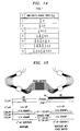
- the interleave chirp for values of P up to 8 is given in Table 1 shown in Fig. 14.
- Switching via a phase shifter unit 170 having connecting waveguides of nominally equal lengths has three significant benefits.
- the dominant loss in WGRs is due to radiation outside of ⁇ 0 as described in the previously-referenced article by C. Dragone, "Optimum design of a planar array of tapered waveguides," J. Opt. Soc. Am. A, vol. 7, pp. 2081-2091 (1990).
- the loss is especially high near the edges of ⁇ 0 , this portion of ⁇ 0 is often even discarded, as discussed in the previously-referenced article by K. Okamoto et. al.
- the addition of connections in ⁇ -1 and ⁇ +1 significantly reduces the losses.
- a well-known limitation of the two-arm Mach-Zehnder as a switch is sensitivity to the exact power splitting ratios of the two couplers This. for example, limited the switching extinction ratio of the add/drop arrangement described in the Okamoto et. al. article, requiring a series of Mach-Zehnders in order to improve the extinction.
- three or more arms per wavelength channel in the interferometer, as in the interleave cross-connect of Fig 1 one can always adjust the phases so as to have exactly zero power in one port provided that the sum of the powers in the arms with the lowest powers is greater than the power in the third.
- this is generally the case.
- a similar argument holds for the case of more than three arms.
- the phase shifters can be adjusted to correct for them. This tolerance is especially useful for designs in media with small waveguide dimensions, such as Indium Phosphide (InP).
- InP Indium Phosphide
- the WDM cross-connect may also be implemented as part of a silica integrated circuit.
- Fig. 9 shows for the arrangement of Fig. 8, the illustrative transmissivity from input line 1 to output line 1 (solid line) and input line 1 to output line 2 (dashed line) of the WDM interleave cross-connect 100 of Fig. 1.
- Fig. 9(a) all connecting waveguide path lengths are equal, except for channel 3, see 901, which has a length long enough to produce the required extra 90° phase shift.
- Fig.9(b) the channel 3 connecting path length is adjusted to achieve best switching extinction ratio.
- the switching extinction ratio in Fig. 9(a) is only ⁇ 20 dB.
- the optimum switching extinction ratio does not occur when the connecting waveguides have exactly the same path length, which is because there is non-negligible power lost to ⁇ -2 ', and ⁇ +2 '.
- Fig. 9(b) shows that for the best switching extinction ratio, the length of the channel 3 waveguide needs to be somewhat more or less than the length needed for an extra 90° phase shift.
- the phase shifters for the images from ⁇ 0 ', ⁇ +1 ', and ⁇ -1 ' have been adjusted to maximize the switching extinction ratio (i.e., a triangle made of the phasors in the three arms was formed).
- the extinction ratio is limited by the sidelobes of the WGR response.
- FIG. 10 there is shown an arrangement where two waveguides 1002 and 1003 are used to connect to each wavelength channel image 1001 in each ⁇ i ' from coupler 112.
- the widths of the connecting waveguides 1002 and 1003 are narrowed along with the spacing between them in order to enhance their mutual coupling to each ⁇ i ' image.
- each of the waveguide grouping 131-134 would contain 6 waveguides (two for each image in ⁇ -1 ' , ⁇ 0 ', and ⁇ +1 ').
- the image 1001 is focused on the region 1004 between the waveguides 1002 and 1003, a portion of the image is still coupled to the waveguides 1002 and 1003.
- Fig. 11(a) shows, for the arrangement of Fig. 10, the illustrative transmissivity from input line 1 to output line 1 (solid line) and input line 1 to output line 2 (dashed line) of the WDM interleave cross-connect 100 of Fig. 1.
- Fig. 11(b) an additional defocusing chirp is added to both the WGRs, 113 and 123, in order to increase the flatness at the tops of the passbands.
- FIG. 12 With reference to Fig. 12 there is shown a close-up of a region 1210 of coupler 112 of WGR 110 of Fig. 1. As shown, this arrangement uses three waveguides 1202, 1203 and 1204 to connect to each wavelength channel image 1201 in each ⁇ i ' from coupler 112. Again the widths of the connecting waveguides 1202 - 1204 are narrowed along with the spacing between them in order to enhance their mutual coupling to each ⁇ i ' from coupler 112. It should be noted that both the widths and spacings of the waveguides 1202-1204 of Fig. 12 are less than the widths and spacings of the waveguides 1002-1003 of Fig. 10.
- each of the waveguide grouping 131-134 of Fig. 1 would contain 9 waveguides (three for each ⁇ -1 ', ⁇ 0 ', and ⁇ +1 '). While the image 1201 is focused on the waveguide 1203, a portion of the image is still coupled to the waveguides 1202 and 1204.
- the transmissivity from input line 1 to output line 1 and input line 1 to output line 2 of the arrangement of Fig. 12 would be similar to that shown in Figs. 11a and 11b, but have a somewhat more rectangular passband that has a higher extinction ratio.
- the coupling between the star-coupler 112 and the one or more waveguides of array 130 used for each channel may be a rectangular passband with very low excess loss as described in the previously-referenced U.S. Patent 5,488,680.
- residual passband ripple e.g., 902 of Fig. 9
- each waveguide group can be placed under a single contact.
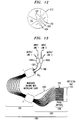
- Fig. 13 Shown in Fig. 13 is an illustrative diagram of a reconfigureable wavelength-division-multiplexing (WDM) cross-connect 1300 comprising an "interleave-chirped" waveguide grating router (WGRs) 1301, a phase shifter unit 1302 , and a reflector unit 1303 and couplers 1304a and 1304b. Since the WDM cross-connect 100 is symmetric about the axis 190, the WDM cross-connect 1300 may be formed by cutting WGR 110 in half, at axis 190, and placing a reflector unit at the axis 190 location. The resulting WDM cross-connect 1300 includes the left-half of Fig.
- WGRs waveguide grating router
- phase shifter unit 1302 is the same as that of the left-half of waveguide array 130 and phase shifters 140.
- the phase shift provided by phase shifters 1306 is only one-half of that provided by phase shifters 140 of Fig. 1.
- the signals from input lines 1 and 2 are coupled via couplers 1304 to WGR 1301.
- WGR 1301 After the wavelength images are demultiplexed and processed by WGR 1301 and pass through the waveguides 1305 and phase shifters 1306 they are reflected by reflector unit 1303. After reflection, the wavelength images obtain another phase shift from phase shifter 1306 (the two phase shifts of phase shifters 1306 equals the phase shift of phase shifters 140).
- the wavelength images then pass through waveguides 1305, are multiplexed by WGR 1301, outputted at either port 1306 or 1307, and then coupled via the appropriate coupler unit 1304a or 1304b to output line 1 or 2, respectively.
- phase shift of phase shifters 1306 are set at a first value (about zero) for one or more wavelengths of a signal from input line 1 (input line 2) these one or more wavelengths are outputted on output line 1 (output line 2), while if the phase shift of phase shifters 1306 are set at a second value (about 90°) for one or more wavelengths then these one or more wavelengths are outputted on output line 2 (output line 1). Note that since the images pass twice through phase shifters 1306, phase shifters need only be shifted by one half the amount that is needed by phase shifters 140. Again the phase shift of phase shifters 1306 are controlled by electrical or optical signals 1310 to each of the phase shifters 1306.
- the waveguides have a normalized transverse index step of 0.85%, and the bend radius is 620 ?m.
- the dimensions of the entire device is about 4.2 x 9.5 mm 2 .
- the waveguide structure is a buried rib as shown in Fig. 15.
- the slab and rib were grown, then the waveguides were wet-etched into the rib. Undoped InP was grown on top.
- a protective layer of SiO2 over the waveguides and between the phase shifters SiO2 width of 33 ?m was applied.
- a p-doped layer was grown over the phase shifters, and finally gold contacts (52 ?m wide) were deposited on the phase shifters.
- the phase shifters are 1.4 mm long, spaced by 85 ?m, and aligned to the ⁇ 110 ⁇ direction.
- Fig. 16 shows a more generalized illustrative diagram of a reconfigureable wavelength-division-multiplexing (WDM) cross-connect of the type shown in Fig. 1 which is implemented using two groups of angular dispersive elements 1601 and 1602 connected by a phase shifter unit 1603.
- the angular dispersive elements 1601 and 1602 may be implemented using a virtually imaged phase array (VIPA) as described in the article by M.
- VIPA virtually imaged phase array
- phase shifter 1603 of Fig. 16 may be implemented in a well-known manner using free space optics.
- a reflector unit may be used to replace the right half of Fig. 16, in the same manner as shown and described in Fig. 13.
- Fig. 17 shows such an arrangement of a reconfigureable WDM cross-connect comprising an angular dispersive elements unit 1701, a phase shifter unit 1702, a reflector unit 1703, and couplers 1704.
- the WDM cross-connect of Fig. 17 operates in essentially the same manner as the WDM cross-connect previously discussed for Fig. 13.
- Couplers 1704 Signals inputted at couplers 1704 enter one or more selected ports of the angular dispersive elements unit 1701 and phase shifter unit 1702 and are reflected back through the phase shifter unit 1703 and angular dispersive elements unit 1701 and, with the appropriate value set in particular phase shifter(s) of phase shifter unit 1703, the reflected signals may be outputted from one or more selected ports of the angular dispersive elements unit 1601 to an output line via couplers 1704.
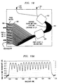
- Fig. 18 shows an add/drop device which is the subject of the present invention.
- the present discussion centers on a add/drop device.
- WGRs waveguide grating routers
- Mach-Zehnder switches Mach-Zehnder switches
- signals from a transmission line 1801 enter the in port and are sent to grating arms 1802 via star coupler .
- the WGR may advantageously be conventional with the exception that every other arm is shortened by ⁇ /4, which is called the "interleave chirp". This causes each wavelength to create two images in each Brillouin zone of the star couplers.
- the two images plus the nearest image outside the center Brillouin zone for each channel are collected by waveguides.
- the signals then pass through the phase shifters 1805, reflect off the partially reflecting mirror 1806 and reenter the grating.
- the portions of the signals that pass through the partial reflector 1806 can be coupled into fibers (not shown). These signals can advantageously be measured as dropped channels. Likewise, channels can be added by sending external signals through the partial reflector 1806. Since there are three ports for each channel to choose from, one would ordinarily choose the port closest to the Brillouin zone center as the drop port, and the second closest as the add port.
- this device varies from a conventional add/drop in that all the channels are always available at the drop ports whether they are actually removed from the line or not.
- the device can also be used to perform network monitoring functions or as a sensor for gain equalization.
- the interleave chirp allows for a reflective design without requiring a circulator nor care to minimize facet reflections.
- a reflective design in turn obviates the need for wavelength-aligning multiple WGRs, significantly reducing the device size and halves the necessary phase shifter turning current.
- the fabrication of my device is simple, since it has no highly critical feature dimensions.
- An exemplary, 16-channel, 100-GHz channel-spacing device similar to that shown in Fig. 18 has been constructed using InP.
- the waveguides are wet-etched rib-loaded slabs buried in 0.7 ⁇ m of undoped InP, and the phase shifters have a p-doped layer grown on top, as shown by.
- an InP cap layer was etched off of the p ++ layer after patterning with 18 ⁇ m-wide openings and prior to metal evaporation.
- the p-doped layer was etched down to 0.4 ⁇ m in a nonselective etch after applying the metals.
- a silicon chip containing gold strip lines was glued to the top of the device using conventional epoxy adhesive, wire bonded from the phase shifters to the gold strip lines, and then wire-bonded from the strip lines to a circuit board with a 50-pin connector.
- the phase shifters can be tuned by either reverse voltage or forward current: +2 ⁇ for +7mA.
- reverse voltage there is no crosstalk between phase shifters, but for forward current, there is some "neighbor heating". Because the three phase shifters for each channel are far apart in a 16-channel device, a small correction had to be applied to neighboring channels when reconfiguring using forward current. Nevertheless, on ly forward current was used so all 32 of the pins were connected to 32 computer-controlled current drivers, two for each channel, leaving the third floating.
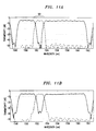
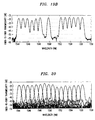
- Fig. 19 shows the measured fiber-to-fiber transmissivity for the TE polarization from the in port to the pass port showing (a) all channels passed and (b) three channels dropped.
- the current values ranged from 0 to 7.3 mA per phase shifter.
- Fig. 4 shows the measured transmissivities from the in port to 16 add/drop ports.
- the nonuniformities in the peak transmissivities in the figures are entirely due to imperfections at certain locations on the facet the 80% multilayer reflection coating. Also the high loss is mainly due to over-doping of p-layer in the phase shifters, which also caused the TM polarazation to exhibit even higher loss.
- One modification is the insertion of a quarter-wave plate with its birefringence axes at 45° to the circuit, between the partial reflector and the phase shifters. This modification eliminates any polarization dependence in the device for the passed channels.
- Another modification is to include two or more collection waveguides per channel image in order to create excess-loss-free rectangular passbands for the passed channels.
- Each set of collection waveguides for each channel image can be grouped under a single phase shifter.
- Yet another modification is to make the in port and the pass port the same waveguide and increase the relfectance of the partial reflector to one or more sets of the collection waveguides and change the interleave chirp (by using less or more than ⁇ /4 length change) so that most of the power is sent to the collection waveguides with the lower partial reflectance.
- the drop ports then couple to the ports of lower partial reflectance. The result is lower loss for the dropped or added ports.
- another modification is to make the device in a material such as silica or polymer and cut slots between the phase shifters (with, for example, a saw or laser).
- tuning the phase shifters by using mechanical stress or strain.
Landscapes
- Physics & Mathematics (AREA)
- Engineering & Computer Science (AREA)
- Microelectronics & Electronic Packaging (AREA)
- General Physics & Mathematics (AREA)
- Optics & Photonics (AREA)
- Optical Integrated Circuits (AREA)
- Optical Communication System (AREA)
Abstract
Description
- This invention relates to Wavelength-Division-Multiplexers (WDMs) and, more particularly, to a WDM programmable add/drop using an interleave-chirped waveguide grating router.
- A Wavelength-Division-Multiplexing (WDM) cross-connect (a non-wavelength-changing one) is a device that can exchange any wavelength channel in any line with the same wavelength channel in any other line. The conventional design is to use a matrix of switches between sets of wavelength multiplexers, such as Waveguide Grating Routers (WGRs). For example see the publications
- [1] M. K. Smit, "New focusing and dispersive planar component based on an optical phased array," Electron. Lett., vol. 24, pp. 385-386 (1988);
- [2] H. Takahashi, S. Suzuki, K. Kato and I. Nishi, "Arrayed-waveguide grating for wavelength division multi/demultiplexer with nanometer resolution," Electron. Lett., vol. 26, pp. 87-88 (1990); and
- [3] C. Dragone, "An N x N optical multiplexer using a planar arrangement of two star couplers," IEEE Photon. Technol. Lett., vol. 3, 812-814 (1991).
-
- For 2 line x 2 line versions, designs have been demonstrated with discrete components {e.g., see B. Glance, "Tunable add drop optical filter providing arbitrary channel arrangements," IEEE Photon. Technol. Lett., vol. 7, 1303-1305 (1995)} and with fully integrated components {e.g., see K. Okamoto, M. Okuno, A. Himeno, and Y. Ohmori, "16-channel optical add/drop multiplexer consisting of arrayed-waveguide gratings and double-gate switches," Electron. Lett., vol. 32, 1471-1472 (1996)}.
- Notwithstanding these advances in the design of WDMs, there is a continuing need for WDM devices which facilitate the transmission and management of optical signals.
- In accordance with the present invention, a Wavelength-Division-Multiplexer (WDM) programmable add/drop is made using an interleave-chirped waveguide grating router and phase shifters in a reflective arrangement.
- More particularly A Wavelength Division Multiplexing (WDM) programmable add/drop device comprising waveguide grating router, a phase shifter unit and a reflective unit are optically connected. This arrangement allows the dropping and adding of optical channels from and to an optical transmission line. Additionally, the arrangement allows for control of relative power of channels passing through the device.
- In the drawings,
- Fig. 1 shows an illustrative diagram of a reconfigureable wavelength-division-multiplexing (WDM) cross-connect comprising two "interleave-chirped" waveguide grating routers (WGRs) connected by a phase shifter unit;
- Fig. 2 shows an illustrative image being focused in a Brillouin zone Ω0 of the free space region of a star coupler of a standard WGR,
- Fig. 3 shows the images from
input line 1 at a free space region of a star coupler when all the even-numbered grating arms remain and the odd-numbered grating arms are removed; - Fig. 4 shows the images from
input line 1 at a free space region of a star coupler when all the odd-numbered grating arms remain and the even-numbered grating arms are removed; - Fig. 5 shows the images from
input line 1 at a free space region of a star coupler when all the odd-numbered grating arms are lengthened to include an additional 90° phase rotation and the even-numbered grating arms are removed; - Fig. 6 shows the combined images from Fig. 3 and Fig. 5 at the free space region of a star coupler when all the odd-numbered grating arms are lengthened to include an additional 90° phase rotation;
- Fig. 7a shows the images from
input line 2 at a free space region of a star coupler when all the odd-numbered grating arms are lengthened to include an additional 90° phase rotation and the even-numbered grating arms are removed; - Fig. 7b shows the combined images from Fig. 4 and Fig. 7a at the free space region of a star coupler when all the odd-numbered grating arms are lengthened to include an additional 90° phase rotation ;
- Fig. 8 shows the free space region of a star coupler having one waveguide for coupling each wavelength image to the phase shifter unit;
- Figs. 9(a) and 9(b) show the transmissivity of different embodiments of the arrangement of Fig. 8;
- Fig. 10 shows the free space region of a star coupler having two waveguides for coupling each wavelength image to the phase shifter unit;
- Fig 11(a) and 11(b) show the transmissivity of different embodiments of the arrangement of Fig. 10;
- Fig. 12 shows the free space region of a star coupler having three waveguides for coupling each wavelength image to the phase shifter unit;
- Fig. 13 shows an illustrative diagram of a reconfigureable WDM cross-connect comprising a "interleave-chirped" WGR, a phase shifter unit, a reflector unit, and couplers;
- Fig. 14 shows a table illustrating the grating arm changes to apply to WGRs when the number of lines P varies from2 through 8;
- Fig. 15 shows an illustrative implementation of a waveguide and a waveguide with phase shifter;
- Fig. 16 shows a more generalized illustrative diagram of a reconfigureable WDM cross-connect comprising two groups of angular dispersive elements connected by a phase shifter unit;
- Fig. 17 shows an illustrative diagram of a reconfigureable WDM cross-connect comprising an angular dispersive elements unit, a phase shifter unit, a reflector unit, and couplers;
- Fig. 18 shows a layout of a programmable add/drop device according to the present invention;
- Fig. 19 shows the measured fiber to fiber transmissivity between an in port and a pass port for (a) all channels passed and (b) three channels dropped; and
- Fig. 20 shows the measured fiber to fiber transmissivity between the in port and sixteen of the add/drop ports.
-
- In the following description, each item or block of each figure has a reference designation associated therewith, the first number of which refers to the figure in which that item is first located (e.g., 110 is first located in FIG. 1).
- Shown in Fig. 1 is an illustrative diagram of a reconfigureable wavelength-division-multiplexing (WDM)
cross-connect 100 comprising two "interleave-chirped" waveguide grating routers (WGRs) 110 and 120 connected by a phase shifter unit 170 which includes awaveguide arrays 130 and 130' and aphase shifter array 140. TheWDM cross-connect 100 can be monolithically integrated with no waveguide crossings and theoretically can achieve very high switching extinction ratios and a nearly excess-loss-free rectangular spectral response. - A plurality of optical lines, e.g.,
lines WDM cross-connect 100. Each of thelines line 1, can be exchanged with the same wavelength channel in the other line, i.e.,line 2. For the more general P line x P line case, where P = 2, the channels can be switched in a cyclical fashion between lines. The WDMcross-connect 100 can be implemented as a compact device with no waveguide crossings; can theoretically achieve very high, fabrication-tolerant, switching extinction ratios; and can theoretically achieve a nearly excess-loss-free rectangular spectral response. - Each of the two "interleave-chirped"
WGRs - For any multiple wavelength signal received over each the
input lines WGR 110 causes all signal wavelengths which are the same to be directed to the same output waveguide ofarrays 130 and 130'. Consequently, each of the different wavelengths ofinput line 1 is received infree space region 114 and directed, according to wavelength, to a particular group of one or more of the waveguides ofarrays 130 and 130'. Similarly, each of the different wavelengths of input line 2 (if spaced within the same Brillouin zones Ω0 as input line 1) is received infree space region 114 and directed, according to wavelength, to a particular group of one or more of the waveguides ofarrays 130 and 130'. Thus in Fig. 1, if we assume that the signal online 1 includes four wavelength channels λ1, λ2, λ3, and λ4 each of the wavelengths would be directed to a different group ofwaveguides array 130. - In accordance with the present invention, for P=2 input and output lines (
lines 1 and 2) the WGR 110 (and 120) are provided with an "interleave chirp" which consists of giving every other grating arm of array 113 (and 123) an additional path length of λc/4, where λc is the wavelength of interest in the waveguide (λc = λc0/n). The additional path length of λc/4 produces a delay or phase shift of π/2, or 90 degrees. The radiation patterns from the arrays of waveguide grating arms, e.g., 113, in thestar couplers WGR 110 have Brillouin zones Ωi of order i and width 2γ [e.g., see the article by C. Dragone, "Optimum design of a planar array of tapered waveguides," J. Opt. Soc. Am. A, vol. 7, pp. 2081-2091 (1990)]. The interleave chirp makes the WGRs create two images for each wavelength in each Ωi, the images spaced by γ. This can be understood from the following: consider a non-chirped WGR. Single-wavelength (or frequency) signals entering an input port, e.g.,input line 1, in onestar coupler 111 of theWGR 110 are imaged to Ω0 in thefree space region 114 of the other star coupler, i.e., 112. - With reference to Fig. 2, there is shown a
λ1 signal image 201 being focused in Brillouin zone Ω0 of thefree space region 114 ofstar coupler 112 of a standard "non-chirped" WGR. While in our example the image was derived for a λ1 signal received oninput line 1, a λ1 signal received overinput line 2 would generate thesame image 206. It should also be noted that a longer wavelengthλ2 entering line 1 would produce theimage 206 in Brillouin zone Ω0. To better understand how theimage 201 is formed, we consider Figs 3 and 4. - Shown in Fig. 3 is a
star coupler 112 where all of the even-numberedgrating arms 301 tostar coupler 112 remain and the odd-numberedgrating arms 302 are removed. In such a modified coupler, the new Brillouin zones Ω0', Ω+1' and Ω-1' are half the size of those of Fig. 2, and there is animage - Shown in Fig. 4 is the effect of putting-back the odd-numbered
arms 302 and removing the even-numberedarms 301. The same Brillouin zones Ω0', Ω+1' and Ω-1' andsame images - It should be noted that when all the
grating arms image 201 in Brillouin zone Ω0· - With reference to Fig. 5, in accordance with the present invention, when an "interleave chirp" is added to the odd-
order grating arms 302, the phasors of the odd-order grating arms 302 are phase shifted or rotated by π/2. As shown in Fig. 5, the resulting images in the Brillouin zones Ωi' (i.e. Ω0', Ω+1' and Ω-1') are counter-clockwise rotated by π/2 (90 degrees) 501, as shown by theimages WGR 112 is formed having all of itsgrating arms 302 connected as shown in Fig. 6, itsimages images images images order images images - As previously noted, if the same single-wavelength signal enters an input port associated with
input line 2, which is spaced by the width of one W' from the input port associated withline 1 instar coupler 111, it would also be imaged to Ω0' in thefree space region 114 ofstar coupler 112. In this example, however, it is the images of Fig. 3 that are rotated and those of Fig. 4 remain the same. The 90 degree rotated images of Fig. 3 are shown in Fig. 7a, by theimages WGR 112 is formed having all of itsgrating arms 302 connected, the rotatedimages images images images images - Returning to Fig. 1, the images out of
WGR 112 are collected by the equal-length waveguides ofarray 130. Generally only images from Ω0', Ω+1' and Ω-1' are connected since they contain almost all the image power. To better show the waveguide sets in Fig. 1, the WGR free-spectral range is 5 channel widths, with the 5th channel unconnected, as one can see from the gaps in the waveguide spacings. Thus, there are three output waveguides, each spaced by y, for each wavelength channel 131 - 134 exitingcoupler 112 ofWGR 110 and enteringcoupler 122 ofWGR 120. Thus as shown in Fig. 1, each of the groups of three waveguides 131 - 134 handle the wavelengths λ1, λ2, λ3, and λ4, respectively. A wavelength channel λ1 entering input line 1 (or input line 2) can be switched to either output line 1 (or output line 2) by controlling the relative phases (via phase shifters 140) between the three connecting waveguides for that channel. For example, channel λ3 which connects viawaveguides 133 to phaseshifter unit 140 has its phase shift controlled by thephase shifter elements phase shifter unit 140. Essentially, each wavelength channel has its own generalized Mach-Zehnder interferometer, consisting of theWGRs arrays 130 and 130' for that channel. - Each of the 12 phase shifter elements of
unit 140 are made to have a controllable phase shift which can be switched between a first value and a second value. The first phase value (e.g., typically about zero) enables the desired wavelength channel received frominput line 1 atWGR 110 to be outputted atoutput line 1 ofWGR 120. The second phase value (e.g., typically provides about 180° phase shift) enables the desired wavelength at ainput line 1 atWGR 110 to be outputted atoutput line 2 ofWGR 120. - Since the operation of the
WDM unit 100 is symmetrical about themiddle line 190, the operation ofWGR 110,waveguide unit 130 and left-half ofphase shifter 140 operates the same as the right-half ofphase shifter 140, waveguide unit 130' andWGR 120. As a result, if the images of wavelength λ1 ofinput line 1 are made to look like images of wavelength λ1 ofinput line 2, they are outputted byWGR 120 tooutput line 2. In this manner in a 2line WDM 100, a wavelength channel from one input line can be switched to another output line and vice-versa. In a more general P line WDM implementation, where P = 2, a wavelength channel λ1 fromline 1 can be switched to anadjacent line 2, a wavelength channel λ1 fromline 2 toline 3 etc. The wavelength channel λ1 of the Pth line can be switched toline 1. - Obviously if a plurality of wavelengths λi of
input line 1 are to be switched fromoutput line 1 tooutput line 2 then the corresponding phase shift elements inunit 140 associated with those plurality of wavelengths λi must be switched to the second phase value. - The phase shifter elements in
array 140 can be made controllable using a an electrical signal, optical signal, or temperature, e.g.,149, to control an optical index of refraction of the associated phase shifter element and thereby change the effective length of that phase shifter element. - The WDM cross-connect design of Fig. 1 can be expanded to the case of P lines x P lines by employing an interleave chirp in the
WGRs channel 1 inline 1 toline 2, thenchannel 1 inline 2 necessarily switches toline 3, andchannel 1 inline 3 necessarily switches toline 1. One cannot exchange channels between lines without affecting that same channel in the other lines. If one requires this functionality, one can build it out of an array of P=2 devices using, for example, a well-known Banyan network [e.g., see the article by L. Goke and G. Lipovski, "Banyan Networks for Partitioning Multiprocessor Systems," Proceedings of the First Annual Symposium on Computer Architecture, pp. 21-28 (1973)]. - Switching via a phase shifter unit 170 having connecting waveguides of nominally equal lengths has three significant benefits. First, the dominant loss in WGRs is due to radiation outside of Ω0 as described in the previously-referenced article by C. Dragone, "Optimum design of a planar array of tapered waveguides," J. Opt. Soc. Am. A, vol. 7, pp. 2081-2091 (1990). The loss is especially high near the edges of Ω0, this portion of Ω0 is often even discarded, as discussed in the previously-referenced article by K. Okamoto et. al. In the interleave cross-connect, the addition of connections in Ω-1 and Ω+1 significantly reduces the losses.
- Second, a well-known limitation of the two-arm Mach-Zehnder as a switch is sensitivity to the exact power splitting ratios of the two couplers This. for example, limited the switching extinction ratio of the add/drop arrangement described in the Okamoto et. al. article, requiring a series of Mach-Zehnders in order to improve the extinction. However, by having three or more arms per wavelength channel in the interferometer, as in the interleave cross-connect of Fig 1, one can always adjust the phases so as to have exactly zero power in one port provided that the sum of the powers in the arms with the lowest powers is greater than the power in the third. In other words, one can always form a triangle from three segments provided that the sum of the lengths of the shorter two segments is greater than the third. For connecting waveguides to Brillouin zones Ω-1', Ω0', and Ω+1', this is generally the case. A similar argument holds for the case of more than three arms. Thus even if there are fabrication imperfections, the phase shifters can be adjusted to correct for them. This tolerance is especially useful for designs in media with small waveguide dimensions, such as Indium Phosphide (InP). It should be noted that the WDM cross-connect may also be implemented as part of a silica integrated circuit.
- Third, in the proposed device, one can use multiple connecting waveguides in each Ωi' for each wavelength channel. With reference to Fig. 8 there is shown an arrangement wherein only one
waveguide 801 is used to connect to eachwavelength channel image 802 in each Ωi' fromcoupler 112. - Fig. 9 shows for the arrangement of Fig. 8, the illustrative transmissivity from
input line 1 to output line 1 (solid line) andinput line 1 to output line 2 (dashed line) of the WDM interleave cross-connect 100 of Fig. 1. In Fig. 9(a) all connecting waveguide path lengths are equal, except forchannel 3, see 901, which has a length long enough to produce the required extra 90° phase shift. In Fig.9(b) thechannel 3 connecting path length is adjusted to achieve best switching extinction ratio. As one can see, the switching extinction ratio in Fig. 9(a) is only ∼20 dB. Thus the optimum switching extinction ratio does not occur when the connecting waveguides have exactly the same path length, which is because there is non-negligible power lost to Ω-2', and Ω+2'. - Fig. 9(b) shows that for the best switching extinction ratio, the length of the
channel 3 waveguide needs to be somewhat more or less than the length needed for an extra 90° phase shift. In Fig. 9(b), the phase shifters for the images from Ω0', Ω+1', and Ω-1' have been adjusted to maximize the switching extinction ratio (i.e., a triangle made of the phasors in the three arms was formed). The extinction ratio is limited by the sidelobes of the WGR response. - With reference to Fig. 10 there is shown an arrangement where two
waveguides wavelength channel image 1001 in each Ωi' fromcoupler 112. The widths of the connectingwaveguides image 1001 is focused on theregion 1004 between thewaveguides waveguides - Fig. 11(a) shows, for the arrangement of Fig. 10, the illustrative transmissivity from
input line 1 to output line 1 (solid line) andinput line 1 to output line 2 (dashed line) of the WDM interleave cross-connect 100 of Fig. 1. In Fig. 11(b) an additional defocusing chirp is added to both the WGRs, 113 and 123, in order to increase the flatness at the tops of the passbands. - With reference to Fig. 12 there is shown a close-up of a
region 1210 ofcoupler 112 ofWGR 110 of Fig. 1. As shown, this arrangement uses threewaveguides wavelength channel image 1201 in each Ωi' fromcoupler 112. Again the widths of the connecting waveguides 1202 - 1204 are narrowed along with the spacing between them in order to enhance their mutual coupling to each Ωi' fromcoupler 112. It should be noted that both the widths and spacings of the waveguides 1202-1204 of Fig. 12 are less than the widths and spacings of the waveguides 1002-1003 of Fig. 10. - Returning to Fig. 12, assuming that only the Brillouin zones Ω-1', Ω0', and Ω+1' are used, we connect waveguides to Ω-1', Ω0', and Ω1', resulting in three connecting waveguides per wavelength channel. Then each of the waveguide grouping 131-134 of Fig. 1 would contain 9 waveguides (three for each Ω-1', Ω0', and Ω+1'). While the
image 1201 is focused on thewaveguide 1203, a portion of the image is still coupled to thewaveguides input line 1 tooutput line 1 andinput line 1 tooutput line 2 of the arrangement of Fig. 12 would be similar to that shown in Figs. 11a and 11b, but have a somewhat more rectangular passband that has a higher extinction ratio. - Thus by careful design, the coupling between the star-
coupler 112 and the one or more waveguides ofarray 130 used for each channel may be a rectangular passband with very low excess loss as described in the previously-referenced U.S. Patent 5,488,680. If necessary, residual passband ripple, e.g., 902 of Fig. 9, can be smoothed out by moving the port waveguides out of focus, which can be done either physically or by chirping the WGRs with the function ε[m - (M+1)/2]2 added to the arm length distribution, where E is a small number with units of length giving some additional loss. Such an approach is described in the article by C. R. Doerr, M. Shirasaki, and C. H. Joyner, "Chromatic focal plane displacement in the parabolic chirped waveguide grating router," IEEE Photon. Technol. Lett., vol. 9, pp. 625-627 (1997). To minimize the number of phase shifter contacts, each waveguide group can be placed under a single contact. - Finally, a design with integrated connecting waveguides prevents the random performance fading due to multipath interference that can occur in large networks containing back-to-back multiplexers connected by fibers, as described in the article by E. L. Goldstein and L. Eskildsen, Scaling limitations in transparent optical networks due to low-level crosstalk, IEEE Photon. Technol. Lett., vol. 7., pp. 93-94 (1995).
- Shown in Fig. 13 is an illustrative diagram of a reconfigureable wavelength-division-multiplexing (WDM) cross-connect 1300 comprising an "interleave-chirped" waveguide grating router (WGRs) 1301, a
phase shifter unit 1302 , and areflector unit 1303 andcouplers axis 190, theWDM cross-connect 1300 may be formed by cuttingWGR 110 in half, ataxis 190, and placing a reflector unit at theaxis 190 location. The resultingWDM cross-connect 1300 includes the left-half of Fig. 1 includingWGR 110, thewaveguide array 130 and the left-half ofphase shifter array 140, i.e., up toline 190. The operation of theWGR 1301 is the same as that ofWGR 130. The operation ofphase shifter unit 1302 is the same as that of the left-half ofwaveguide array 130 andphase shifters 140. Thus, the phase shift provided by phase shifters 1306 is only one-half of that provided byphase shifters 140 of Fig. 1. - The signals from
input lines WGR 1301. After the wavelength images are demultiplexed and processed byWGR 1301 and pass through thewaveguides 1305 and phase shifters 1306 they are reflected byreflector unit 1303. After reflection, the wavelength images obtain another phase shift from phase shifter 1306 (the two phase shifts of phase shifters 1306 equals the phase shift of phase shifters 140). The wavelength images then pass throughwaveguides 1305, are multiplexed byWGR 1301, outputted at eitherport 1306 or 1307, and then coupled via theappropriate coupler unit output line phase shifters 140. Again the phase shift of phase shifters 1306 are controlled by electrical oroptical signals 1310 to each of the phase shifters 1306. - Fig. 15 shows an illustrative implementation of a waveguide and a waveguide with phase shifter. More particularly, Fig. 15 shows a 2 line x 2 line, 6-channel x 200 GHz spacing cross connect in InP. M1 = M2 = 30, and the WGRs have free-spectral-ranges of 7 x 200 GHz. The connecting waveguides are connected to ?-1', ?0', and ?1' for each channel (?i' are the Brillouin zones of the star couplers in the WGRs[4]), resulting in a total of 3 x 6 = 18 connecting waveguides. To account for any relative wavelength shift between the two WGRs, several ports were included at each line connection. The waveguides have a normalized transverse index step of 0.85%, and the bend radius is 620 ?m. The dimensions of the entire device is about 4.2 x 9.5 mm2.
- The waveguide structure is a buried rib as shown in Fig. 15. First, the slab and rib were grown, then the waveguides were wet-etched into the rib. Undoped InP was grown on top. Then a protective layer of SiO2 over the waveguides and between the phase shifters (SiO2 width of 33 ?m) was applied. Then a p-doped layer was grown over the phase shifters, and finally gold contacts (52 ?m wide) were deposited on the phase shifters. The phase shifters are 1.4 mm long, spaced by 85 ?m, and aligned to the 〈110〉 direction.
- While the present invention has been described in Fig. 1 as using WGR ,e.g., 110 and 120, it should be understood that the
units dispersive elements phase shifter unit 1603. The angulardispersive elements phase shifter 1603 of Fig. 16, as well as thephase shifter unit 140 of Fig. 1, may be implemented in a well-known manner using free space optics. - It should also be noted that because of the symmetry of Fig. 16, a reflector unit may be used to replace the right half of Fig. 16, in the same manner as shown and described in Fig. 13. Fig. 17 shows such an arrangement of a reconfigureable WDM cross-connect comprising an angular
dispersive elements unit 1701, aphase shifter unit 1702, a reflector unit 1703, andcouplers 1704. The WDM cross-connect of Fig. 17 operates in essentially the same manner as the WDM cross-connect previously discussed for Fig. 13. Signals inputted atcouplers 1704 enter one or more selected ports of the angulardispersive elements unit 1701 andphase shifter unit 1702 and are reflected back through the phase shifter unit 1703 and angulardispersive elements unit 1701 and, with the appropriate value set in particular phase shifter(s) of phase shifter unit 1703, the reflected signals may be outputted from one or more selected ports of the angulardispersive elements unit 1601 to an output line viacouplers 1704. - With reference now to Fig. 18 there it shows an add/drop device which is the subject of the present invention. As can be appreciated by those skilled in the art, while the previous discussion pertained to a WDM cross-connect, the present discussion centers on a add/drop device.
- As those skilled in the art will quickly appreciate, it is desirable to have devices that can remove any number of wavelength channels from a wavelength-division multiplexed transmission line and provide the channels already demultiplexed to a dropping station. The device must be programmable such that the dropping station can choose at any time which channels to drop without affecting uninvolved channels. For integrated devices, designs have been demonstrated in silica and InP using waveguide grating routers (WGRs) and Mach-Zehnder switches. In contrast to these, our subject invention is based on an interleave chirped WGR.
- With continued reference to Fig. 18, signals from a
transmission line 1801 enter the in port and are sent to gratingarms 1802 via star coupler . The WGR may advantageously be conventional with the exception that every other arm is shortened by λ/4, which is called the "interleave chirp". This causes each wavelength to create two images in each Brillouin zone of the star couplers. In thelower star coupler 1804, the two images plus the nearest image outside the center Brillouin zone for each channel are collected by waveguides. Thus, there are three collection waveguides per channel, with all the collection waveguides equal in length. The signals then pass through thephase shifters 1805, reflect off the partially reflectingmirror 1806 and reenter the grating. They are then sent either back to the inport 1801 or to the "pass" port or some combination thereof; depending upon the phase shifter settings. Since there are three phase shifters per channel, one can always perfectly null the signal being sent to one of the ports provided that the sum of the powers in the two lower-power ports is greater than that in the third. Channels are dropped by nulling them in the pass port. - The portions of the signals that pass through the
partial reflector 1806 can be coupled into fibers (not shown). These signals can advantageously be measured as dropped channels. Likewise, channels can be added by sending external signals through thepartial reflector 1806. Since there are three ports for each channel to choose from, one would ordinarily choose the port closest to the Brillouin zone center as the drop port, and the second closest as the add port. - Note that this device varies from a conventional add/drop in that all the channels are always available at the drop ports whether they are actually removed from the line or not. Thus the device can also be used to perform network monitoring functions or as a sensor for gain equalization.
- As those skilled in the art will quickly appreciate, the advantages associated with my design are numerous. First, the interleave chirp allows for a reflective design without requiring a circulator nor care to minimize facet reflections. A reflective design in turn obviates the need for wavelength-aligning multiple WGRs, significantly reducing the device size and halves the necessary phase shifter turning current. Second, the fabrication of my device is simple, since it has no highly critical feature dimensions. Third, there are no waveguide crossings employed with my design. Finally, because some of the light that falls outside the central Brillouin zone of the second star coupler is collected, reduces the loss and makes the loss nearly the same for all channels.
- An exemplary, 16-channel, 100-GHz channel-spacing device similar to that shown in Fig. 18 has been constructed using InP. The device utilized 76 grating arms, had a grating free-spectrum range of 18 x 100 GHz, and phase shifters 850 µm long with a spacing of 85 µm.
- The fabrication of the device is straightforward. Specifically, the waveguides are wet-etched rib-loaded slabs buried in 0.7 µm of undoped InP, and the phase shifters have a p-doped layer grown on top, as shown by. To make a pristine surface to get the required uniform junction over the phase shifters, an InP cap layer was etched off of the p++ layer after patterning with 18 µm-wide openings and prior to metal evaporation. In order to increase the current confinement, the p-doped layer was etched down to 0.4 µm in a nonselective etch after applying the metals. Finally, a silicon chip containing gold strip lines was glued to the top of the device using conventional epoxy adhesive, wire bonded from the phase shifters to the gold strip lines, and then wire-bonded from the strip lines to a circuit board with a 50-pin connector.
- The phase shifters can be tuned by either reverse voltage or forward current: +2π for +7mA. For reverse voltage, there is no crosstalk between phase shifters, but for forward current, there is some "neighbor heating". Because the three phase shifters for each channel are far apart in a 16-channel device, a small correction had to be applied to neighboring channels when reconfiguring using forward current. Nevertheless, on ly forward current was used so all 32 of the pins were connected to 32 computer-controlled current drivers, two for each channel, leaving the third floating.
- Fig. 19 shows the measured fiber-to-fiber transmissivity for the TE polarization from the in port to the pass port showing (a) all channels passed and (b) three channels dropped. The current values ranged from 0 to 7.3 mA per phase shifter. Fig. 4 shows the measured transmissivities from the in port to 16 add/drop ports. The nonuniformities in the peak transmissivities in the figures are entirely due to imperfections at certain locations on the facet the 80% multilayer reflection coating. Also the high loss is mainly due to over-doping of p-layer in the phase shifters, which also caused the TM polarazation to exhibit even higher loss.
- As can be further appreciated, several modifications can be made to improve the performance for certain applications. One modification is the insertion of a quarter-wave plate with its birefringence axes at 45° to the circuit, between the partial reflector and the phase shifters. This modification eliminates any polarization dependence in the device for the passed channels.
- Another modification is to include two or more collection waveguides per channel image in order to create excess-loss-free rectangular passbands for the passed channels. Each set of collection waveguides for each channel image can be grouped under a single phase shifter.
- Yet another modification is to make the in port and the pass port the same waveguide and increase the relfectance of the partial reflector to one or more sets of the collection waveguides and change the interleave chirp (by using less or more than λ/4 length change) so that most of the power is sent to the collection waveguides with the lower partial reflectance.
- The drop ports then couple to the ports of lower partial reflectance. The result is lower loss for the dropped or added ports. Finally, another modification is to make the device in a material such as silica or polymer and cut slots between the phase shifters (with, for example, a saw or laser). One could then consider tuning the phase shifters by using mechanical stress or strain. Also, one could remove the substrate under the "freed" phase shifters reducing the thermal loading and thus the required phase shifting power.
- Thus, what has been described is merely illustrative of the application of the principles of the present invention. Other arrangements and methods can be implemented by those skilled in the art without departing from the scope of the present invention.
Claims (17)
- A Wavelength Division Multiplexing programmable add/drop device comprising:such that optical signals may be selectively added or dropped.a first unit including 2 or more wavelength demultiplexers that couple substantially equally to one or more input ports;a phase shifter unit that carries optical signals to and from the demultiplexers of the first unit and a partial reflector unit; andthe partial reflector unit which:partially reflects the optical signals back to the first unit such that each reflected optical signal is directed back to a particular input port by the phase shifter; andpartially transmits demultiplexed optical signals;
- The Wavelength Division Multiplexing programmable add/drop device according to claim 1 wherein said first unit includes:a first coupler having at least an "in" port and a "pass" port at one end, whereby optical signals including one or more optical wavelengths enter the device through the "in" port and whereby optical signals including one or more optical wavelengths exit the device through the "pass" port; and a plurality of ports at an end other than the one end;an interconnect unit including a plurality of waveguides substantially and uniformly increasing in path length except for an interleave chirp consisting of shortening or lengthening every other waveguide by a fixed amount L; the waveguides interconnecting the said plurality of ports of the first coupler to a plurality of ports of a second coupler; andsaid second coupler having a plurality of ports at one end, and another plurality of ports at an other end, the second said plurality of ports receiving demultiplexed optical signals and there are two or more ports for each optical wavelength of interest:
- The Wavelength Division Multiplexing programmable add/drop device according to claim 2 wherein said phase shifter unit is optically connected to said waveguide grating router and includes:a plurality of phase shifter waveguides for interconnecting said second plurality of ports of said second coupler to a plurality of phase shifters; andthe plurality of phase shifters, each providing a tunable phase shift to the optical signals passing therethrough.
- The Wavelength Division Multiplexing programmable add/drop device according to claim 3 further comprising:a reflector unit optically connected to said phase shifter, said reflector unit including:a partial reflector for reflecting optical signals back through said phase shifter unit and said waveguide grating router; anda means for coupling optical signals in to and out from the phase shifter waveguides through the partial reflector unit.
- The Wavelength Division Multiplexing programmable add/drop device according to claim 1 further comprising:
a quarter-wavelength plate having its birefringence axis at substantially 45 degrees to the optical circuit, said quarter-wavelength plate being positioned between the partial reflector and phase shifter unit. - A Wavelength Division Multiplexing (WDM) programmable add/drop device comprising:a waveguide grating router including:a first coupler having at least an "in" port and a "pass" port at one end, whereby optical signals including one or more optical wavelengths enter the device through the "in" port and whereby optical signals including one or more optical wavelengths exit the device through the "pass" port; and a plurality of ports at an end other than the one end;an interconnect unit including a plurality of waveguides substantially and uniformly increasing in path length except for an interleave chirp consisting of shortening or lengthening every other waveguide by a fixed amount L; the waveguides interconnecting the said plurality of ports of the first coupler to a plurality of ports of a second coupler; andsaid second coupler having a plurality of ports at one end, and another plurality of ports at an other end, the second said plurality of ports receiving demultiplexed optical signals and there are two or more ports for each optical wavelength of interest:a phase shifter unit optically connected to said waveguide grating router; said phase shifter unit including:a plurality of phase shifter waveguides for interconnecting said second plurality of ports of said second coupler to a plurality of phase shifters; andthe plurality of phase shifters, each providing a tunable phase shift to the optical signals passing therethrough; anda reflector unit optically connected to said phase shifter, said reflector unit including:a partial reflector for reflecting optical signals back through said phase shifter unit and said waveguide grating router;a means for coupling optical signals in to and out from the phase shifter waveguides through the partial reflector unit.
- The WDM add/drop device of claim 7 further comprising:
a quarter-wavelength plate with its birefringence axis at 45 degrees to the optical circuit is placed between the partial reflector and phase shifter unit. - The WDM add/drop device of claim 7 wherein the "in" and "pass" ports are contained within same waveguide
- The WDM add/drop device of claim 7 wherein the "in" and "pass" ports are contained within different waveguides
- The WDM add/drop device of claim 7 wherein said add/drop is implemented as part of a silica optical integrated circuit
- The WDM add/drop device of claim 7 wherein said add/drop is implemented as part of an indium phosphide integrated circuit
- The WDM add/drop device of claim 7 wherein cuts are made between the phase shifters.
- The WDM add/drop device of claim 7 wherein the phase shifters are thermooptic .
- The WDM add/drop deviceof claim 13 wherein cuts are made between the phase shifters, and the substrate is all or partially removed from underneath the phase shifters to reduce the thermal loading.
- The WDM add/drop of claim 13 wherein the phase shifters tune via mechanical stress.
- The WDM add/drop of claim 7 wherein L is substantially equal to a quarter of a wavelength.
- The WDM add/drop of claim 7 wherein the value of the partial reflectance is not the same for all phase shifter waveguides.
Applications Claiming Priority (2)
| Application Number | Priority Date | Filing Date | Title |
|---|---|---|---|
| US09/040,781 US6141467A (en) | 1998-03-18 | 1998-03-18 | Wavelength-division-multiplexing programmable add/drop using interleave-chirped waveguide grating router |
| US40781 | 1998-03-18 |
Publications (2)
| Publication Number | Publication Date |
|---|---|
| EP0963072A2 true EP0963072A2 (en) | 1999-12-08 |
| EP0963072A3 EP0963072A3 (en) | 2000-01-12 |
Family
ID=21912906
Family Applications (1)
| Application Number | Title | Priority Date | Filing Date |
|---|---|---|---|
| EP99301792A Withdrawn EP0963072A3 (en) | 1998-03-18 | 1999-03-09 | Wavelength-division-multiplexing progammable add/drop using interleave-chirped waveguide grating router |
Country Status (3)
| Country | Link |
|---|---|
| US (1) | US6141467A (en) |
| EP (1) | EP0963072A3 (en) |
| JP (1) | JPH11326851A (en) |
Cited By (1)
| Publication number | Priority date | Publication date | Assignee | Title |
|---|---|---|---|---|
| WO2003098856A3 (en) * | 2002-05-20 | 2004-03-04 | Metconnex Inc | Reconfigurable optical add-drop module, system and method |
Families Citing this family (27)
| Publication number | Priority date | Publication date | Assignee | Title |
|---|---|---|---|---|
| TW472024B (en) * | 1997-06-18 | 2002-01-11 | Corning Corp | A method of positioning a broken fiber for threading |
| JP3895480B2 (en) * | 1998-09-25 | 2007-03-22 | 古河電気工業株式会社 | Optical wavelength multiplexer / demultiplexer |
| KR100327898B1 (en) * | 1998-11-12 | 2002-08-21 | 한국전자통신연구원 | Wavelength Demultiplexer without Waveguide Bending Loss |
| US6307991B1 (en) * | 1999-07-28 | 2001-10-23 | Corning Incorporated | Optical filter with harmonic elements |
| US6256433B1 (en) * | 1999-09-24 | 2001-07-03 | Wavesplitter Technologies, Inc. | Expandable interleaving optical add/drop filter module |
| KR20010061613A (en) * | 1999-12-28 | 2001-07-07 | 윤종용 | Node structure of wavelength division multiplexing system for modular upgradabilty |
| US20010046350A1 (en) * | 2000-02-25 | 2001-11-29 | Tedesco James M. | Configurable Wavelength routing device |
| US6980740B1 (en) * | 2000-06-22 | 2005-12-27 | Lucent Technologies Inc. | Apparatus for detecting raman gain in an optical transmission system |
| US6349158B1 (en) * | 2000-10-05 | 2002-02-19 | Tera Fiberoptics, Inc | Hybrid cascade structure for DWDM |
| US6690855B2 (en) * | 2000-12-15 | 2004-02-10 | Nortel Networks Limited | Planar waveguide dispersion compensator |
| US6731833B2 (en) | 2001-01-16 | 2004-05-04 | T-Rex Enterprises Corp. | Optical cross connect switch |
| US6907167B2 (en) | 2001-01-19 | 2005-06-14 | Gazillion Bits, Inc. | Optical interleaving with enhanced spectral response and reduced polarization sensitivity |
| US6766074B1 (en) | 2001-08-15 | 2004-07-20 | Corning Incorporated | Demultiplexer/multiplexer with a controlled variable path length device |
| IL145320A (en) * | 2001-09-06 | 2006-12-10 | Gilad Optical Switches Ltd | Tunable optical filter |
| US7171067B2 (en) * | 2003-03-03 | 2007-01-30 | Lucent Technologies Inc. | Integrateable optical interleaver and de-interleaver |
| US6873763B2 (en) * | 2002-04-12 | 2005-03-29 | Intel Corporation | Managing channels with different wavelengths in optical networks |
| JP4150374B2 (en) * | 2003-02-26 | 2008-09-17 | 富士通株式会社 | Arrayed waveguide type wavelength multiplexer / demultiplexer |
| US6836600B2 (en) * | 2003-03-13 | 2004-12-28 | Lucent Technologies Inc. | Optical coupler with low loss interconnections |
| US9530132B2 (en) * | 2004-01-27 | 2016-12-27 | George Chester Cox | System and method for customer video authentication to prevent identity theft |
| JP4634815B2 (en) * | 2005-02-09 | 2011-02-16 | 日本電信電話株式会社 | Optical filter |
| US7373039B1 (en) * | 2006-12-28 | 2008-05-13 | Lucent Technologies Inc. | Low-ripple optical device |
| US9372214B2 (en) * | 2011-06-03 | 2016-06-21 | Cascade Microtech, Inc. | High frequency interconnect structures, electronic assemblies that utilize high frequency interconnect structures, and methods of operating the same |
| WO2015135003A2 (en) * | 2014-03-04 | 2015-09-11 | California Institute Of Technology | Directional optical receiver |
| US10488589B2 (en) * | 2017-02-08 | 2019-11-26 | Rockley Photonics Limited | T-shaped arrayed waveguide grating |
| EP4024100A1 (en) | 2017-07-17 | 2022-07-06 | Rockley Photonics Limited | Athermalized multi-path interference filter |
| US11294061B1 (en) * | 2017-08-18 | 2022-04-05 | Acacia Communications, Inc. | LiDAR sensor with orthogonal arrays |
| CN116996796B (en) * | 2023-09-27 | 2023-12-22 | 北京邮电大学 | Array waveguide grating router based on staggered chirp array and optical routing method |
Citations (2)
| Publication number | Priority date | Publication date | Assignee | Title |
|---|---|---|---|---|
| US5396507A (en) * | 1993-11-15 | 1995-03-07 | At&T Corp. | Reflective digitally tunable laser |
| EP0826989A2 (en) * | 1996-09-02 | 1998-03-04 | Nippon Telegraph And Telephone Corporation | Optical signal processing apparatus and optical signal processing method |
Family Cites Families (2)
| Publication number | Priority date | Publication date | Assignee | Title |
|---|---|---|---|---|
| US5136671A (en) * | 1991-08-21 | 1992-08-04 | At&T Bell Laboratories | Optical switch, multiplexer, and demultiplexer |
| FR2753803B1 (en) * | 1996-09-24 | 1998-12-11 | MULTIPLEXER COMPONENT WITH SPECTROGRAPH WITH WAVEGUID ARRAY |
-
1998
- 1998-03-18 US US09/040,781 patent/US6141467A/en not_active Expired - Lifetime
-
1999
- 1999-03-09 EP EP99301792A patent/EP0963072A3/en not_active Withdrawn
- 1999-03-17 JP JP11072681A patent/JPH11326851A/en active Pending
Patent Citations (2)
| Publication number | Priority date | Publication date | Assignee | Title |
|---|---|---|---|---|
| US5396507A (en) * | 1993-11-15 | 1995-03-07 | At&T Corp. | Reflective digitally tunable laser |
| EP0826989A2 (en) * | 1996-09-02 | 1998-03-04 | Nippon Telegraph And Telephone Corporation | Optical signal processing apparatus and optical signal processing method |
Non-Patent Citations (2)
| Title |
|---|
| DOERR C R ET AL: "Wavelength-division multiplexing cross connect in InP" IEEE PHOTONICS TECHNOLOGY LETTERS, IEEE, USA, vol. 10, no. 1, January 1998 (1998-01), pages 117-119, XP002122684 ISSN: 1041-1135 * |
| ZIRNGIBL M ET AL: "DIGITALLY TUNABLE CHANNEL DROPPING FILTER/EQUALIZER BASED ON WAVEGUIDE GRATING ROUTER AND OPTICAL AMPLIFIER INTEGRATION" IEEE PHOTONICS TECHNOLOGY LETTERS,US,IEEE INC. NEW YORK, vol. 6, no. 4, page 513-515 XP000446610 ISSN: 1041-1135 * |
Cited By (2)
| Publication number | Priority date | Publication date | Assignee | Title |
|---|---|---|---|---|
| WO2003098856A3 (en) * | 2002-05-20 | 2004-03-04 | Metconnex Inc | Reconfigurable optical add-drop module, system and method |
| US7236660B2 (en) | 2002-05-20 | 2007-06-26 | Jds Uniphase Corporation | Reconfigurable optical add-drop module, system and method |
Also Published As
| Publication number | Publication date |
|---|---|
| JPH11326851A (en) | 1999-11-26 |
| US6141467A (en) | 2000-10-31 |
| EP0963072A3 (en) | 2000-01-12 |
Similar Documents
| Publication | Publication Date | Title |
|---|---|---|
| US6141467A (en) | Wavelength-division-multiplexing programmable add/drop using interleave-chirped waveguide grating router | |
| EP0901024B1 (en) | Wavelength-division-multiplexing cross-connect using angular dispersive elements and phase shifters | |
| JP3537344B2 (en) | Optical add-drop multiplexer | |
| US6263127B1 (en) | Free-space/arrayed-waveguide router | |
| US5982960A (en) | Optical wavelength multiplexer/demultiplexer | |
| EP0911659B1 (en) | Optical add/drop multiplexer having complementary stages | |
| US6421478B1 (en) | Tapered MMI coupler | |
| EP0919005B1 (en) | Optical multiplexer/demultiplexer | |
| JP5117104B2 (en) | Asymmetric Mach-Zehnder interferometer with reduced drive voltage coupled to a small low-loss arrayed-waveguide grating | |
| JPH11160742A (en) | Optical filter | |
| US6266460B1 (en) | Large-channel-count programmable wavelength add-drop | |
| US6243514B1 (en) | Optical multiplexer/demultiplexer | |
| US6587615B1 (en) | Wavelength multiplexer-demultiplexer having a wide flat response within the spectral passband | |
| Doerr et al. | 40-wavelength add drop filter | |
| Doerr et al. | Wavelength-division multiplexing cross connect in InP | |
| US6956987B2 (en) | Planar lightwave wavelength blocker devices using micromachines | |
| KR20020055445A (en) | Arrayed waveguide grating type otpical multiplexer/demultiplexer | |
| Doerr | Proposed WDM cross connect using a planar arrangement of waveguide grating routers and phase shifters | |
| TW202318051A (en) | On-chip integrated wavelength division multiplexer and chip | |
| US6993217B2 (en) | Optical switch device | |
| Doerr et al. | Arrayed waveguide lens wavelength add-drop in silica | |
| US20020176660A1 (en) | Optical wavelength multiplexer/demultiplexer and use method thereof | |
| US6801690B1 (en) | Grating-based wavelength selective switch | |
| US20020081062A1 (en) | Optical grating based multi-input demultiplexer for multiple sets of interleaved wavelength channels | |
| US20020131692A1 (en) | Miniaturized reconfigurable DWDM add/drop system for optical communication system |
Legal Events
| Date | Code | Title | Description |
|---|---|---|---|
| PUAI | Public reference made under article 153(3) epc to a published international application that has entered the european phase |
Free format text: ORIGINAL CODE: 0009012 |
|
| PUAL | Search report despatched |
Free format text: ORIGINAL CODE: 0009013 |
|
| AK | Designated contracting states |
Kind code of ref document: A2 Designated state(s): DE ES FR GB IT |
|
| AX | Request for extension of the european patent |
Free format text: AL;LT;LV;MK;RO;SI |
|
| AK | Designated contracting states |
Kind code of ref document: A3 Designated state(s): AT BE CH CY DE DK ES FI FR GB GR IE IT LI LU MC NL PT SE |
|
| AX | Request for extension of the european patent |
Free format text: AL;LT;LV;MK;RO;SI |
|
| RIC1 | Information provided on ipc code assigned before grant |
Free format text: 7H 04J 14/02 A, 7G 02B 6/34 B, 7G 02B 6/293 B |
|
| 17P | Request for examination filed |
Effective date: 20000630 |
|
| AKX | Designation fees paid |
Free format text: DE ES FR GB IT |
|
| RAP1 | Party data changed (applicant data changed or rights of an application transferred) |
Owner name: AGERE SYSTEMS OPTOELECTRONICS GUARDIAN CORPORATION |
|
| STAA | Information on the status of an ep patent application or granted ep patent |
Free format text: STATUS: THE APPLICATION IS DEEMED TO BE WITHDRAWN |
|
| 18D | Application deemed to be withdrawn |
Effective date: 20031001 |