EP0961529A2 - Printed wiring board comprising an insect repellent and method of manufacturing the same - Google Patents
Printed wiring board comprising an insect repellent and method of manufacturing the same Download PDFInfo
- Publication number
- EP0961529A2 EP0961529A2 EP99110151A EP99110151A EP0961529A2 EP 0961529 A2 EP0961529 A2 EP 0961529A2 EP 99110151 A EP99110151 A EP 99110151A EP 99110151 A EP99110151 A EP 99110151A EP 0961529 A2 EP0961529 A2 EP 0961529A2
- Authority
- EP
- European Patent Office
- Prior art keywords
- electronic material
- curing
- repellent
- provisionally
- paint
- Prior art date
- Legal status (The legal status is an assumption and is not a legal conclusion. Google has not performed a legal analysis and makes no representation as to the accuracy of the status listed.)
- Granted
Links
Images


Classifications
-
- H—ELECTRICITY
- H05—ELECTRIC TECHNIQUES NOT OTHERWISE PROVIDED FOR
- H05K—PRINTED CIRCUITS; CASINGS OR CONSTRUCTIONAL DETAILS OF ELECTRIC APPARATUS; MANUFACTURE OF ASSEMBLAGES OF ELECTRICAL COMPONENTS
- H05K3/00—Apparatus or processes for manufacturing printed circuits
- H05K3/22—Secondary treatment of printed circuits
- H05K3/28—Applying non-metallic protective coatings
- H05K3/285—Permanent coating compositions
Definitions
- the present invention relates to a printed wiring board used in general electronic appliance for household use or business use.
- a printed wiring board of the invention comprises:
- a manufacturing method of a printed wiring board of the invention comprises:
- This constitution hence suppresses invading or staying of insects having sensory nerves such as cockroaches and ants in the printed wiring board. It hence prevents troubles of electronic appliances due to dead bodies or wastes of these insects. As a result, the reliability of electronic appliances is enhanced. It further prevents thickness fluctuation or blurring of the repellent layer of the electronic material mixing the repellent.
- the printed wiring board of the invention is free from warp or other abnormal appearance. By using the printed wiring board of the invention, occurrence of detects is decreased in the process of mounting the parts. Further, the productivity is enhanced. The printing wiring board having all these effects is obtained. Thus, without sacrificing the repellent effect, the productivity is enhanced, the quality is improved, and the cost is reduced.
- a printed wiring board in an embodiment of the invention comprises an insulating substrate, a conductive layer and an insulting layer formed on the insulating substrate, and an electronic material as a paint containing a repellent placed on the insulating substrate having the conductive layer and insulating layer, and the electronic material is applied and formed selectively.
- the repellent effect is exhibited efficiently, and the repellent effect is maintained, so that a stable repellent effect is obtained.
- thickness fluctuations are decreased and blurring is decreased in the electronic material containing the repellent, and moreover warp of the printed wiring board is decreased.
- the quality of the printed wiring board is enhanced.
- the printed wiring board of the invention has the following constitution.
- the printed wiring board has a parts layout, and the electronic material containing the repellent is placed on the printed wiring board having the parts layout. In this constitution, loss of the repellent due to heat in the curing process of the parts layout is prevented, and the above effects are particularly exhibited.
- the printed wiring board comprises an electronic material containing a repellent, and a parts layout placed in the printed wiring board having such electronic material. In this constitution, the discernibility of the parts layout is enhanced.
- the electronic material containing the repellent is disposed in a wider area on the surface of the printed wiring board on the side mounting parts, than on the side not mounting parts.
- insects prefer the narrower place, the darker place, and the warmer place. Insects are likely to invade or nest in such component side.
- the repellent effect may be efficiently enhanced.
- the ratio of the area of electronic material on the component side to the area of electronic material on the solder side is 100 to about 30 to about 90. In this constitution, the effects are further enhanced.
- the concentration of the repellent in the electronic material is changed between the surface side and back side depending on the mounting method, configuration of parts or types of parts. In this constitution, the repellent effect may be efficiently enhanced.
- the concentration of the repellent in the electronic material is higher on the solder side. In this constitution, the repellent is gradually lost due to heat of soldering, but if the repellent is decreased, lowering of the repellent effect may be prevented.
- the concentration of the repellent in the electronic material is higher on the side mounting more heat generating parts such as semiconductors. In this constitution, invasion and nesting of insects preferring the warmer place can be efficiently prevented.
- the ratio of the concentration of the repellent in the electronic material on the solder side to the opposite side is 100 to about 30 to about 80.
- the repellent is gradually lost by the heat of soldering, since the concentration of the repellent in the electronic material on the solder flow side is higher, lowering of the repellent effect is prevented.
- the ratio of the concentration of the repellent in the electronic material on the side mounting more heat generating parts to the opposite side is 100 to about 50 to about 80. In this constitution, invasion and nesting of insects preferring the warmer place can be efficiently prevented.
- the electronic material containing the repellent is applied and formed. In this constitution, the repellent effect may be efficiently enhanced.
- the electronic material containing a higher concentration of the repellent is applied and formed. In this constitution, the repellent effect may be efficiently enhanced.
- the electronic material containing the repellent is applied and formed in a concentric pattern. In this constitution, the repellent effect may be enhanced.
- the electronic material containing the repellent is applied and formed in a concentric pattern, and the density of the concentric pattern is higher in the positions closer to the heat generating parts.
- the repellent effect may be efficiently enhanced.
- the concentration of the repellent in the electronic material is higher in the position closer to the heat generating parts such as semiconductors likely to be inhabited by the insects preferring the warmer place. In this constitution, the repellent effect may be efficiently enhanced.
- the electronic material containing the repellent is applied and formed in a region excluding immediately beneath the surface mount parts. In this constitution, troubles in parts mounting process are prevented.
- the electronic material containing the repellent is applied and formed in mesh.
- the repellent effect is exhibited effectively, and the total loss of the repellent is decreased.
- the quality is improved, the productivity is enhanced, and the cost is reduced.
- defects in the mounting process of the user are decreased.
- the electronic material containing the repellent is applied and formed in stripes depending on the mounting position and mounting state of parts.
- the repellent effect is exhibited effectively, the quality and productivity are enhanced, and defects in the mounting process of parts are decreased.
- the electronic material containing the repellent is applied and formed in dots.
- the repellent effect is exhibited effectively, the quality and productivity are enhanced, and defects in the mounting process of parts are decreased.
- the consumption of the electronic material containing the repellent is saved, so that the cost is reduced.
- the electronic material containing the repellent is applied and formed in a concentric pattern from the center of the substrate. In this constitution, the repellent effect may be efficiently enhanced.
- the electronic material containing the repellent is applied and formed in a film around the end of the substrate. In this constitution, invasion of insects onto the substrate is prevented, so that the repellent effect may be efficiently enhanced.
- the concentration of the repellent in the electronic material is higher in the periphery of the substrate. In this constitution, invasion of insects onto the substrate is prevented, so that the repellent effect may be efficiently enhanced.
- the electronic material is formed in a circular dot form.
- the antennae and legs of insects may contact securely with the electronic material.
- the repellent effect is exhibited effectively, warp of the printed wiring board is decreased, the quality and productivity are enhanced, and defects in the parts mounting process are decreased. Further, the consumption of the electronic material containing the repellent is decreased, so that the cost is reduced.
- the film pitch of the electronic material containing the repellent is formed at about 1 to about 20 mm depending on the size of the insects to be repelled.
- the antennae and legs of insects may contact securely with the electronic material.
- the repellent effect may be efficiently enhanced.
- the film density of the electronic material containing the repellent is higher in the periphery of the substrate. In this constitution, invasion of insects onto the substrate is prevented, and the repellent effect may be efficiently enhanced.
- a manufacturing method of a printed wiring board of the invention comprises (a) a step of forming a conductive layer and an insulating layer in at least one side of an insulating substrate, (b) a step of applying an electronic material as a paint containing a repellent selectively on an insulating substrate having the conductive layer and insulating layer, and (c) a step of curing the electronic material.
- thickness fluctuation and blurring of the electronic material containing the repellent are prevented. Further, warp of the printed wiring board is decreased. Thus, the quality and productivity are enhanced. Further, the consumption of the electronic material containing the repellent is decreased, so that the cost is reduced. Moreover, defects in the parts mounting process are decreased.
- the step of selectively applying and curing the electronic material containing the repellent in the constitution in which the soldering side is a first surface of the electronic material, it is intended to prevent slight deterioration of the repellent effect due to loss of the repellent due to heat in the curing step. Further, the repellent effect is exhibited effectively.
- the manufacturing condition in the step of selectively applying the electronic material containing the repellent and the step of curing, on the printed wiring board having a surface side and a back side has different manufacturing conditions on the surface side and back side.
- the loss of the repellent is decreased, and the repellent effect is exhibited effectively.
- the repellent effect is further enhanced.
- thickness fluctuation and blurring of the electronic material containing the repellent are decreased.
- warp of the printed wiring board is decreased.
- the quality and productivity are enhanced, and defects decreased in the parts mounting process.
- the loss of the repellent is suppressed, and then the other side is heated.
- loss of the repellent due to heat in the curing process is prevented, and deterioration of the repellent effect is prevented.
- the repellent effect is enhanced by decrease of loss of the repellent.
- the electronic material is cured provisionally, and then the parts layout is applied, and this parts layout is subsequently used in the curing step and the electronic material is cured completely.
- it is effective to prevent loss of the repellent due to heat in the curing step of the parts layout, and prevent deterioration of the repellent effect.
- the loss of the repellent is decreased, and the repellent effect is exhibited effectively. Further, warp of the printed wiring board is decreased. Thus, the quality and productivity are enhanced.
- a step of plating a noble metal is provided before the step of selectively applying the electronic material containing the repellent and the step of curing. In this constitution, the loss of the repellent due to the plating step is prevented.
- a step of applying a conductive paste and a step of curing the conductive paste are provided before the step of selectively applying the electronic material containing the repellent and the step of curing. In this constitution, the loss of the repellent due to forming of the conductive paste is prevented.
- the step of curing the electronic material containing the repellent first by provisionally curing the first surface by heat of about 50 to 90%, the loss of the repellent is suppressed, and then the second surface is heated.
- the loss of the repellent is suppressed, and then the second surface is heated.
- the repellent effect is exhibited effectively.
- warp of the printed wiring board is decreased.
- the quality and productivity are enhanced.
- the electronic material containing the repellent on the first surface is first cured provisionally by heat of 40 to 80% of the ordinary heat, and then the heat is applied for forming the parts layout and conductive paste.
- the loss of the repellent by the previous heat is decreased, and further the loss of the repellent by the heat applied for forming the parts layout and conductive paste is suppressed. As a result, the repellent effect is enhanced.
- the electronic material on the face surface and back surface is cured provisionally by heat of about 40 to about 80% of the ordinary heat, and then the heat is applied for forming the parts layout.
- the loss of the repellent by the heat in the curing step is suppressed.
- the repellent effect is enhanced.
- a parts layout is formed on a first surface, and then an electronic material containing a repellent is formed.
- a parts layout is applied on other second surface, and this parts layout is provisionally cured by heat of about 60 to 95% of the ordinary heat, and then the electronic material containing the repellent is formed.
- the loss of the repellent contained in the electronic material on the first surface is suppressed.
- the repellent effect is exhibited effectively.
- warp of the printed wiring board is decreased.
- the quality and productivity are enhanced.
- a parts layout is applied on a first surface, and this parts layout is provisionally cured by heat of about 50 to about 85% of the ordinary heat, then an electronic material containing a repellent is formed.
- a solder resist is applied, and this solder resist is provisionally cured by heat of about 70 to about95% of the ordinary heat, and a parts layout is applied, and this parts layout is provisionally cured by heat of about 60% to about 95% of the ordinary heat.
- the heat when forming the solder resist and parts layout on the face surface and back surface can be lowered. Therefore, the loss of the repellent in this process is decreased. As a result, the repellent effect is exhibited effectively. Moreover, warp of the printed wiring board is decreased. Thus, the quality and productivity are enhanced.
- a solder resist is applied on the first surface, and this solder resist is provisionally cured by heat of about 60 to about 85% of the ordinary heat, and then the electronic material is formed.
- the heat when forming the solder resist can be lowered and the loss of the repellent is further suppressed.
- the repellent effect is exhibited effectively.
- warp of the printed wiring board is decreased.
- the quality and productivity are enhanced.
- An electronic material containing a repellent is formed on a first surface, and then a parts layout is applied, and this parts layout is provisionally cured by heat of about 50 to about 85% of the ordinary heat.
- An electronic material containing a repellent is formed on other second surface and then a parts layout is formed.
- the heat when forming the parts layout on the first surface can be lowered, and it is less vulnerable to the effect of heat of the second surface. Therefore, the loss of the repellent is suppressed, and the repellent effect is exhibited effectively. Moreover, warp of the printed wiring board is decreased. Thus, the quality and productivity are enhanced.
- thermosetting type containing a repellent on face surface and back surface is cured, and then a parts layout of ultraviolet curing type is formed.
- an electronic material of ultraviolet curing type containing a repellent is cured, and then a parts layout of thermosetting type is formed.
- the electronic material and the parts layout have mutually different curing steps. In this constitution, warp of the printed wiring board is decreased. As a result, the quality and productivity are enhanced.
- the electronic component containing the repellent is cured by ultraviolet rays.
- the productivity is enhanced.
- the first surface is provisionally cured by the integrated quantity of light of about 55 to about 95% of the ordinary quantity of light. In this constitution, the loss of the repellent is suppressed, and the repellent effect is exhibited effectively.
- An electronic material containing a repellent is formed on a first surface, and then a parts layout is applied, and this parts layout is provisionally cured by heat of about 50 to about 85%.
- a solder resist is applied on other second surface and this solder resist is provisionally cured by heat of 70 to 95%. Then, the electronic material containing the repellent is formed, and then the parts layout is formed.
- the electronic material, solder resist and parts layout after completely forming the first surface, the second surface is formed, and further when forming the parts layout on the second surface, the electronic material, solder resist of the first surface and the electronic material on the second surface are fully cured. In this constitution, the productivity is enhanced, the cost is reduced, and the loss of the repellent is suppressed. As a result, the repellent effect is exhibited effectively.
- a solder resist is applied on the first surface, and this solder resist is provisionally cured by heat of about 60 to about 85% of the ordinary heat, and then the electronic material containing the repellent is formed.
- this solder resist is provisionally cured by heat of about 60 to about 85% of the ordinary heat, and then the electronic material containing the repellent is formed.
- the electronic material containing the repellent on the first surface is provisionally cured by the ultraviolet ray in the integrated quantity of light of about 45 to about 85%. In this constitution, the loss of the repellent is suppressed, and the repellent effect is exhibited effectively.
- the electronic material on the face surface and back surface is provisionally cured by the integrated quantity of light of about 45 to about 85%, and in the subsequent step of forming the parts layout, different curing processes of thermosetting type and ultraviolet curing type are selected.
- the productivity is enhanced.
- the loss of the repellent by heat is suppressed.
- the repellent effect is exhibited effectively.
- a parts layout is formed on a first surface, then an electronic material containing a repellent is applied, and this electronic material is provisionally cured by ultraviolet rays by the integrated quantity of light of about 45 to about 85%.
- a parts layout is applied on a second surface, and the parts is provisionally cured by the integrated quantity of light of about 65 to about 95%, then an electronic material containing a repellent is formed.
- effects of heat when forming the parts layout can be avoided, and the loss of the repellent is suppressed.
- the repellent effect is exhibited effectively.
- warp of the printed circuit board is decreased.
- the quality is enhanced, and the productivity by ultraviolet ray curing is enhanced.
- a parts layout is formed on a first surface, and the parts layout is provisionally cured by the integrated quantity of light of 55 to 90%.
- a solder resist is applied, and the solder resist is provisionally cured by the integrated quantity of light of 75 to 95%, then a parts layout is applied, and the parts layout is provisionally cured by the integrated quantity of light of 65 to 95%.
- an electronic material containing a repellent is applied, and cured.
- a solder resist is applied, and the solder resist is provisionally cured by the integrated quantity of light of about 65 to about 90%.
- the heat effect in curing can be suppressed much lower. Accordingly, the loss of the repellent is further prevented. As a result, the repellent effect is exhibited effectively, and warp of the printed wiring board is decreased. Thus, the quality and productivity are enhanced.
- An electronic material is formed on a first surface, then a parts layout is applied, and the parts layout is provisionally cured by the integrated quantity of light of about 55 to about 90%.
- On a second surface an electronic material is formed and then a parts layout is formed.
- the electronic materials on the face surface and back surface are provisionally cured by the integrated quantity of light of about 45 to about 85%.
- the loss of the repellent due to the integrated quantity of light in the subsequent curing step is suppressed. Accordingly, the repellent effect is exhibited effectively, and warp of the printed wiring board is decreased. Thus, the quality is improved and the productivity is enhanced.
- the electronic materials on the face surface and back surface are provisionally cured by the integrated quantity of light of about 45 to about 85%.
- a solder resist is applied, and is provisionally cured by the integrated quantity of light of about 75 to about 95%.
- the loss of the repellent due to heat effect when forming the solder resist is suppressed.
- the repellent effect is exhibited effectively, and warp of the printed wiring board is decreased.
- the quality and productivity are enhanced.
- the antennae and legs of insects having sensory nerves have a cuticular surface.
- stimulation by the neurotransmitter chemical through the skin is given only to insects having sensory nerves, and these insects are repelled.
- the neurotransmitter chemical unlike the olfactory stimulant, is not required to heighten the vapor pressure of the chemical. Hence, wasteful evaporation or dissipation of the chemical can be suppressed, and the performance lasts for a long period.
- by the learning effect of insects having sensory nerves such as cockroaches and ants by repeating this repellent action several times, nesting of insects can be prevented.
- the repellent is mixed in the resin paste as a foreign matter, blurring is likely to occur in the formed electronic material.
- the formed repellent film is likely to have thickness fluctuations, blurring or warp due to restrictions in the manufacturing conditions. In the embodiment, however, since the electronic material is applied and formed selectively, such defects are eliminated.
- the constitution of the invention prevents deterioration of reliability due to invasion of insects having sensory nerves such as cockroaches and ants into the electronic appliances.
- the electronic material containing the repellent is applied selectively, and the electronic material is cured, the loss of the repellent is decreased.
- the repellent effect is exhibited effectively, and the repellent effect is enhanced.
- It is further effective to decrease the occurrence of thickness fluctuation and blurring of the electronic material containing the repellent.
- warping of the printed wiring board is decreased.
- the quality is improved, the productivity is enhanced, and the cost is reduced.
- defects in the mounting process of the user are decreased.
- the reliability of the printed wiring board is enhanced.
- the electronic material is mainly composed of a repellent and a binder, and the binder contains resin, solvent, filler, pigment, hardener, catalyst and others properly as required.
- a paint containing a repellent and a binder is applied on the substrate.
- This paint may also contain a solvent, and this solvent is evaporated and removed at the time of curing.
- the method of application is generally a method of printing.
- the hardened and formed electronic material comprises the repellent and the binder, not containing solvent.
- the electronic material before curing may contain a solvent.
- the insulating substrate refers to either an insulating layer or an insulating base material.
- the parts layout, paste, and solder resist are formed on the insulating substrate by using ordinary materials. For example, these paints are applied on the insulating substrate, and then cured.
- the parts layout, paste, and solder resist refer to either the state before curing or the cured state.
- Methods of curing the electronic material, parts layout, paste, and solder resist include heating method, and ultraviolet or other light irradiation method.
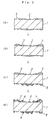
- Fig. 1 shows a manufacturing process of one-side copper filled printed wiring board in an embodiment of the invention.
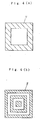
- Fig. 2 (a) and Fig. 2 (b) show application patterns of electronic material.
- the electronic materials containing the repellent are formed on the face surface and back surface.
- the electronic material formed on the face surface and the electronic material formed on the back surface have mutually different repellent concentrations, and have mutually different curing processes.
- a conductive layer 2 is formed as a specified copper foil.
- a thermosetting solder resist 3 is applied on the conductive layer 2, and is cured.
- thermosetting parts layout 4 is applied on the solder resist 3 having a first surface as a soldering surface, and a thermosetting parts layout 4 is further applied on a second surface of the insulating layer 1 for mounting parts.
- the thermosetting parts layouts 4 applied on both surfaces are cured.
- thermosetting solder resist 3 As shown in Fig. 1 (c), a first electronic material 5 containing a repellent by concentration of 35 wt.% is applied on the thermosetting solder resist 3 and thermosetting parts layout 4 on the first surface of soldering (solder flow) side, in stripes as shown in Fig. 2 (a).
- the first electronic material 5 is then provisionally cured in a hot stove in the condition of 160°C and 25 minutes, by heat of about 50 to about 90% of the ordinary curing heat.
- a second electronic material 6 containing a repellent by concentration of 25 wt.% is applied on the thermosetting parts layout 4 formed on the second surface, in mesh as shown in Fig. 2 (b).
- the second electronic material 6 is fully cured in the hot stove in the condition of 160°C and 35 minutes.
- the first electronic material 5 is also cured fully.
- the second electronic material 6 has the repellent concentration of about 30 to 80% of the first electronic material 5.
- the printed wiring board is fabricated.
- a step of forming the conductive paste or a step of forming a noble metal plating is added before formation of the first electronic material 5 and second electronic material 6.
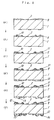
- Fig. 3 shows a manufacturing process of both-side copper filled printed wiring board in other embodiment of the invention.
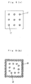
- Fig. 4 (a) and Fig. 4 (b) show application patterns of electronic material.
- the electronic materials containing different concentrations of the repellent are formed on the face surface and back surface.
- the electronic material formed on the face surface and the electronic material formed on the back surface are cured in mutually different thermosetting curing processes.
- thermosetting solder resist 3 is applied to cover the conductive layer 2 except for the soldering area of the solder side and component side, and this thermosetting solder resist 3 is cured.
- a third electronic material 7 containing 20 wt.% of repellent is applied on the thermosetting solder resist 3 on a first surface, in a shape as shown in Fig. 4 (a), in a band form around the end surface of the substrate.
- the third electronic material 7 is provisionally cured in a hot stove in the condition of 160°C and 25 minutes, by about 40% to about 80% of the ordinary curing heat of 160°C and 35 minutes.
- the number of heat generating electronic components mounted on the first surface is smaller than the number of heat generating electronic components mounted on the second surface.
- Heat generating electronic components are, for example, semiconductors.
- a fourth electronic material 8 containing 30 wt.% of repellent is applied on the thermosetting solder resist 3 on the second surface, in a concentric pattern from the center of the substrate as shown in Fig. 4 (b) so as not to be disposed beneath the mounted parts.
- the fourth electronic material 8 is then provisionally cured in the hot stove in the condition of 160°C and 25 minutes, by about 40 to about 80% of the ordinary curing heat of 160°C and 35 minutes.
- the content of the repellent contained in the third electronic material 7 is about 50 to about 80% of the content of the repellent contained in the fourth electronic material 8.
- thermosetting parts layouts 4 are applied on the thermosetting solder resist 3 and third electronic material 7 placed on the first surface and the fourth electronic material 8 and solder resist 3 placed on the second surface.
- the thermosetting parts layouts 4 are cured.
- the printed wiring board is fabricated.
- the concentration may be decreased gradually from the peripheral area to the center, for example, the concentration of the repellent in the third and fourth electronic materials 7, 8 formed around the substrate is about 30 wt.%, and the concentration of the repellent in the third and fourth electronic materials 7, 8 formed in the center of the substrate is about 15 wt.%.
- the same repellent effects are obtained.
- the film density may be lower from the center of the semiconductor or other heat generating electronic component toward the peripheral parts. That is, the film density means the shape of narrowing of interval of concentric lines as approaching the center. In this constitution, the repellent effects are improved.
- Such concentric patterns may include circle, polygon, quadrangle, and any arbitrary shape.
- Fig. 5 shows a manufacturing process of both-side copper filled printed wiring board in a different embodiment of the invention.
- Fig. 6 (a) and Fig. 6 (b) show application patterns of electronic material.
- the electronic material on the face surface and the electronic material on the back surface are applied in mutually different areas, and these electronic materials are cured in mutually different ultraviolet curing processes.
- a conductive layer 2 is formed as a specified copper foil.
- An ultraviolet curing type solder resist 9 is applied to cover the conductive layer 2 except for the soldering area, and this ultraviolet curing type solder resist 9 is cured provisionally in an ultraviolet curing oven at 800 mJ/cm 2 , by about 65 to about 90% of the ordinary integrated quantity of light of 1000 mJ/cm 2 .
- an ultraviolet curing type parts layout 10 is applied on the ultraviolet curing type solder resist 9, and this ultraviolet curing type parts layout 10 is cured provisionally in the ultraviolet curing oven at 800 mJ/cm 2 , by about 55 to about 90% of the ordinary integrated quantity of light of 1000 mJ/cm 2 .
- a fifth electronic material 11 containing a repellent is applied on the ultraviolet curing type solder resist 9 and the ultraviolet curing type parts layout 10 having a first surface as a soldering surface, in dots of 1 mm in diameter at pitches of 4 mm, in about 30 to about 90% of the application area as shown in Fig. 6 (a).
- the fifth electronic material 11 is cured provisionally in the ultraviolet curing oven at 1000 mJ/cm 2 , by about 45 to about 85% of the curing heat of the second surface.
- an ultraviolet curing type solder resist 12 is applied, and this ultraviolet curing type solder resist 12 is cured provisionally in the ultraviolet curing oven at 900 mJ/cm 2 , by about 75 to about 95% of the ordinary integrated quantity of light of 1000 mJ/cm 2 .
- an ultraviolet curing type parts layout 13 is applied on the ultraviolet curing type solder resist 12 on the second surface, and this ultraviolet curing type parts layout 13 is cured provisionally in the ultraviolet curing oven at 900 mJ/cm 2 , by about 65 to about 95% of the ordinary integrated quantity of light of 1000 mJ/cm 2 .
- a sixth electronic material 14 containing a repellent is applied on the ultraviolet curing type solder resist 12 and the ultraviolet curing type parts layout 13 on the second surface, in dots of 1 mm in diameter at pitches of 2 mm as shown in Fig. 6 (b), and this sixth electronic material 14 is cured fully in the ultraviolet curing oven at 1500 mJ/cm 2 .
- the solder resist 9, parts layout 10, fifth electronic material 11, solder resist 12, and parts layout 13 are fully cured.
- the printed wiring board is fabricated.
- the electronic material having high concentration of repellent may be disposed from the center of the location of heat generating parts such as semiconductors. In this constitution, the repellent effect is further enhanced.
- Fig. 7 shows a both-side copper filled printed wiring board in other different embodiment of the invention.
- Fig. 8 (a) and Fig. 8 (b) show application patterns of electronic material.
- the electronic material placed on the face surface and the electronic material placed on the back surface have mutually different areas. These electronic materials are cured in mutually different ultraviolet curing processes.
- a conductive layer 2 is formed as a specified copper foil.
- An ultraviolet curing type solder resist 9 is applied to cover the conductive layer 2 except for the soldering area. This ultraviolet curing type solder resist 9 is cured provisionally in an ultraviolet curing oven at 800 mJ/cm 2 , by about 60 to about 85% of the ordinary integrated quantity of light of 1000 mJ/cm 2 .
- a fifth electronic material 11 is applied on the ultraviolet curing type solder resist 9 placed on the first surface, in dots of 1 mm in diameter at pitches of 4 mm, in about 30 to about 90% of the application area as shown in Fig. 8 (a), and the fifth electronic material 11 is cured provisionally in the ultraviolet curing oven at 1000 mJ/cm 2 , by about 45 to about 85% of the ordinary curing heat.
- an ultraviolet curing type parts layout 10 is applied on the ultraviolet curing type solder resist 9 and the fifth electronic material 11 on the first surface, and this ultraviolet curing type parts layout 10 is cured provisionally in the ultraviolet curing oven at 800 mJ/cm 2 , by about 50 to about 85% of the ordinary integrated quantity of light of 1000 mJ/cm 2 .
- an ultraviolet curing type solder resist 12 is applied, and this ultraviolet curing type solder resist 12 is cured provisionally in the ultraviolet curing oven at 900 mJ/cm 2 , by about 70 to about 90% of the ordinary integrated quantity of light of 1000 mJ/cm 2 .
- a sixth electronic material 14 is applied on the ultraviolet curing type solder resist 12 on the second surface in a shape as shown in Fig. 8 (b).
- the shape is dots of 1 mm in diameter at pitches of 1.5 mm around the substrate, and dots of 1 mm in diameter at pitches of 3 mm in the center of the substrate, so that the film density is inclined.
- the sixth electronic material 14 is cured provisionally in the ultraviolet curing oven in the condition of 1000 mJ/cm 2 , by about 45 to about 85% of the ordinary curing head of the sixth electronic material 14.
- an ultraviolet curing type parts layout 13 is applied on the ultraviolet curing type solder resist 12 and the sixth electronic material 14 of ultraviolet curing type on the second surface, and this ultraviolet curing type parts layout 13 is cured fully in the ultraviolet curing oven at 1000 mJ/cm 2 .
- the printed wiring board is fabricated.
- provisional curing means an incomplete state of curing.
- ordinary curing heat or “ordinary integrated quantity of light” means the heat or integrated quantity of light necessary for complete curing.
- the curing condition such as the curing time and integrated quantity of light is controlled, but not limited to this, for example, the degree of curing may be controlled.
- provisional curing at 60% of ordinary heat means “curing up to 60% of the completely cured state.”
- provisional curing at 70% of ordinary integrated quantity of light means “curing up to 70% of the completed cured state.” Therefore, for provisional curing, the degree of curing of the material may be controlled by control of curing temperature, control of quantity of light irradiation, or control of irradiation time.
- penetration holes may be formed in the insulating substrates, and the electronic components may be mounted by passing through these penetration holes.
- the main body of the electronic component is placed at the second surface side, and the connection terminal of the electronic component is connected to the conductive layer placed on the first surface through its penetration hole.
- the connection terminal of the electronic component is connected to the conductive layer placed on the first surface, and the main body of the electronic component is placed at its first surface side.
- the side mounting the electronic component is the side mounting the electronic component main body.
- the product yield about the blurring and thickness fluctuation was improved by about 10 to 15% as compared with the printed wiring boards applying and forming the electronic materials on the entire surface in the prior art. There was no defect in the parts mounting process due to warp of printed wiring board.
- the insect repellent performance was evaluated by using cockroaches as insects.
- the electronic material containing the repellent was formed on the entire surface except for the soldering land on the surface of the printed wiring boards, and printed wiring boards (B) were prepared.
- printed wiring boards (C) were prepared without forming the electronic materials.
- the cockroach repellent performance was evaluated as follows.
- a paper shelter (nest) and a container of drinking water are placed.
- printed wiring boards of the embodiments selectively forming the electronic material containing the repellent, and uncoated printed wiring boards are placed. German cockroaches are put in the vat.
- the weight loss of cube sugar put on the printed wiring boards (PWB) of the invention was 40 mg to 44 mg.
- the weight loss of cube sugar was 41 mg to 46 mg.
- the weight loss of cube sugar was 290 mg to 310 mg.
- the printed wiring boards of the invention selectively forming the electronic material containing the repellent were free from warp, thickness fluctuation, blurring or other abnormality.
- the printed wiring boards of the invention selectively forming the electronic material containing the repellent were proved to be equivalent or even superior in the cockroach repellent effect, as compared with the conventional printed wiring boards (B) forming on the entire surface. Further as compared with the conventional printed wiring boards (C) without repellent, the printed wiring boards of the invention present a notably excellent insect repellent effect.
- the printed wiring boards of the invention selectively forming the insect repellent layer have same or better insect repellent effects as compared with the conventional printed wiring boards having the insect repellent layer formed on the entire surface.
- the printed wiring boards of the invention are free from warp or other abnormality in appearance. By using the printed wiring boards of the invention, occurrence of defects in the process of mounting parts are decreased. The productivity is further enhanced.
Landscapes
- Engineering & Computer Science (AREA)
- Manufacturing & Machinery (AREA)
- Microelectronics & Electronic Packaging (AREA)
- Non-Metallic Protective Coatings For Printed Circuits (AREA)
- Electric Connection Of Electric Components To Printed Circuits (AREA)
- Catching Or Destruction (AREA)
Abstract
Description
- 1
- Insulating layer (base material)
- 2
- Conductive layer
- 3
- Thermosetting solder resist
- 4
- Thermosetting parts layout
- 5
- Electronic material with 35 wt.% content of thermosetting repellent (first electronic material)
- 6
- Electronic material with 25 wt.% content of thermosetting repellent (second electronic material)
- 7
- Electronic material with 20 wt.% content of thermosetting repellent (third electronic material)
- 8
- Electronic material with 30 wt.% content of thermosetting repellent (fourth electronic material)
- 9
- Ultraviolet curing solder resist on solder side
- 10
- Ultraviolet curing parts layout on solder side
- 11
- Electronic material with ultraviolet curing repellent on solder side (fifth electronic material)
- 12
- Ultraviolet curing solder resist on component side
- 13
- Ultraviolet curing parts layout on component side
- 14
- Electronic material with ultraviolet curing repellent on component side (sixth electronic material)
| Type of PWB | Weight loss of cube sugar (mg) | ||
| PWB of invention | PWB of prior art (B) | PWB of prior art (C) | |
| PWB in Fig. 1 | 40.5 | 41.2 | 292 |
| PWB in Fig. 2 | 43.7 | 45.3 | 311 |
| PWB in Fig. 3 | 41.9 | 43.8 | 308 |
| PWB in Fig. 4 | 41.1 | 42.4 | 297 |
Claims (52)
- A printed wiring board comprising:an insulating substrate having a first surface and a second surface,a conductive layer and an insulting layer formed on at least one of said first surface and said second surface, andan electronic material formed on at least one of said first surface and said second surface of said insulating substrate having said conductive layer and said insulating layer,
wherein said electronic material contains a repellent having an insect repelling performance and a binder, andsaid electronic material is formed with a selective pattern. - A printed wiring board of claim 1,
wherein said repellent is a sensory nerve stimulant having a property of giving stimulation to sensory nerves of said insects. - A printed wiring board of claim 1,
wherein said selective pattern of said electronic material is a parts layout. - A printed wiring board of claim 1, further comprising a parts layout,
wherein said parts layout is formed on said insulating substrate having said electronic material. - A printed wiring board of claim 1, further comprising an electronic component placed on said second surface,
wherein said electronic material has a first pattern placed on said first surface, anda second pattern placed on said second surface, and said second pattern has a wider area than said first pattern. - A printed wiring board of claim 5,
wherein an area of said first pattern to an area of said second pattern is 100 to about 30 to about 90. - A printed wiring board of claim 1,
wherein said electronic material has a first electronic material placed on said first surface, and a second electronic material placed on said second surface, anda concentration of said repellent contained in said first electronic material is different from a concentration of said repellent contained in said second electronic material. - A printed wiring board of claim 1,
wherein said electronic material is placed on both said first surface and said second surface,one of said first surface and second surface has a soldering land, andthe electronic material placed at a surface having said soldering land has a higher concentration of said repellent than the electronic material placed on other surface. - A printed wiring board of claim 1, further comprising a plurality of heat generating electronic components mounted on said first surface and second surface,
wherein said electronic material is placed on both said first surface and said second surface, andthe electronic material placed at a surface having more heat generating electronic components has a higher concentration of said repellent than the electronic material placed on other surface. - A printed wiring board of claim 1,
wherein one of said first surface and second surface has a solder flow part,said electronic material is placed on both said first surface and said second surface, anda concentration of the repellent contained in the electronic material placed at a surface having said solder flow part and a concentration of the repellent contained in the electronic material placed on the other surface are in the relation of 100 to about 30 to about 80. - A printed wiring board of claim 1, further comprising a plurality of heat generating electronic components mounted on said first surface and second surface,
wherein said electronic material is placed on both said first surface and said second surface, anda concentration of the repellent contained in the electronic material placed at a surface mounting more heat generating electronic components and a concentration of the repellent contained in the electronic material placed on the other surface are in the relation of 100 to about 50 to about 80. - A printed wiring board of claim 1, further comprising an electronic component placed at least in one of said first surface and second surface,
wherein said electronic component has a heat generating electronic part, andsaid electronic material is formed around said heat generating electronic part. - A printed wiring board of claim 1, further comprising an electronic component placed on at least one of said first surface and said second surface,
wherein said electronic component has a heat generating electronic part,said selective pattern of said electronic material has a peripheral part of said heat generating electronic part, and a remote part from said heat generating electronic part, anda concentration of the repellent contained in the electronic material formed in said peripheral part is higher than a concentration of the repellent contained in the electronic material formed at said remote part. - A printed wiring board of claim 1, further comprising an electronic component placed on at least one of said first surface and second surface,
wherein said electronic component has a heat generating electronic part, andsaid selective pattern of said electronic material has a concentric pattern around a center of said heat generating part. - A printed wiring board of claim 14,
wherein said concentric pattern has a profile having a film density becoming higher as approaching the center. - A printed wiring board of claim 14,
wherein said electronic material has said concentric pattern containing the repellent at higher concentration as approaching the center. - A printed wiring board of claim 1, further comprising an electronic component placed on at least one of said first surface and said second surface,
wherein said electronic material disposed in a region excluding immediately beneath said electronic component. - A printed wiring board of claim 1,
wherein said selective pattern is formed in mesh. - A printed wiring board of claim 1,
wherein said selective pattern is formed in stripes. - A printed wiring board of claim 1,
wherein said selective pattern is formed in dots. - A printed wiring board of claim 1,
wherein said selective pattern is a concentric pattern formed in a center of said insulating substrate. - A printed wiring board of claim 1,
wherein said selective pattern is a band form formed in a peripheral area of said insulating substrate. - A printed wiring board of claim 1,
wherein said selective pattern is formed in a peripheral part of said insulating substrate and inside of said peripheral part, anda concentration of the repellent contained in the electronic material formed in said peripheral part is higher than a concentration of the repellent contained in the electronic material formed in said inside part. - A printed wiring board of claim 1,
wherein said selective pattern is a circular dot shape. - A printed wiring board of claim 1,
wherein said selective pattern is at least one shape selected from the group consisting of mesh pattern, stripe pattern, dot pattern, and concentric pattern,said shape has a plurality of patterns, anda pitch between patterns of said plurality of patterns is about 1 to about 20 mm. - A printed wiring board of claim 1,
wherein said selective pattern is at least one shape selected from the group consisting of mesh pattern, stripe pattern, dot pattern, and concentric pattern,said shape has a plurality of patterns, andsaid electronic material forming a pattern disposed outside of the plurality of patterns has a higher repellent concentration than the electronic material forming a pattern disposed inside. - A manufacturing method of a printed wiring board comprising the steps of:(a) placing a conductive layer on at least one of a first surface and a second surface of an insulating substrate,(b) placing an insulating layer so as to cover said conductive layer, and(c) forming an electronic material containing a repellent having an insect repelling performance and a binder, on at least one of said first surface and said second surface, with a selective pattern.
- A manufacturing method of a printed wiring board of claim 27,
wherein said step (c) includes:(1) applying a paint containing said repellent and said binder on said surface, and(2) curing said applied paint to form said pattern of said electronic material. - A manufacturing method of a printed wiring board of claim 27,
wherein said conductive layer has a soldering part disposed on said first surface. - A manufacturing method of a printed wiring board of claim 27,
wherein said electronic material has a first electronic material and a second electronic material, said step (c) includes:(1) applying a first paint containing said repellent and said binder on said first surface,(2) curing said first paint to form said first electronic material,(3) applying a second paint containing said repellent and said binder on said second surface, and(4) curing said second paint to form said second electronic material,
wherein said step of curing the first paint and said step of curing the second paint are cured in mutually different conditions. - A manufacturing method of a printed wiring board of claim 28,
wherein said electronic material has a first electronic material and a second electronic material,said step (c) includes:(1) applying a first paint containing said repellent and said binder on said first surface,(2) provisionally curing said first paint to form said first electronic material in provisionally cured state,(3) applying a second paint containing said repellent and said binder on said second surface, and(4) fully curing said second paint to form said second electronic material,
wherein said first electronic material in provisionally cured state is also cured fully, when said second paint is fully cured. - A manufacturing method of a printed wiring board of claim 28,
wherein said step (c) includes:(1) applying a paint containing said repellent and said binder,(2) provisionally curing said applied paint to form said electronic material in provisionally cured state,(3) applying a parts layout on at least one of said first surface and second surface, and(4) fully curing said applied parts layout,
wherein said electronic material in provisionally cured state is also cured fully, when said parts layout is fully cured. - A manufacturing method of a printed wiring board of claim 28, further comprising a step of forming a noble metal plating on said conductive layer before forming said electronic material.
- A manufacturing method of a printed wiring board of claim 28, further comprisinga step of applying a conductive paste on said conductive layer anda step of curing said conductive paste before forming said electronic material.
- A manufacturing method of a printed wiring board of claim 28,
wherein said electronic material has a first electronic material and a second electronic material,said step (c) includes:(1) applying a first paint containing said repellent and said binder on said first surface, and provisionally curing said first paint by heat of about 50% to about 90% of the necessary heat for curing fully to form said first electronic material in provisionally cured state, and(2) applying a second paint containing said repellent and said binder on said second surface, and fully curing said second paint to form said second electronic material, and
wherein said first electronic material in provisionally cured state is also cured fully, when said second paint is fully cured. - A manufacturing method of a printed wiring board of claim 28,
wherein said electronic material has a first electronic material and a second electronic material,said step (c) includes:(1) applying a first paint containing said repellent and said binder on said first surface, and provisionally curing said applied first paint by heat of about 40% to about 80% of the necessary heat for curing fully to form said first electronic material in provisionally cured state, and(2) applying a second paint containing said repellent and said binder on said second surface, and a step of fully curing said applied second paint to form said second electronic material,
wherein said first electronic material in provisionally cured state is also cured fully, when said second paint is fully cured. - A manufacturing method of a printed wiring board of claim 28,
wherein said electronic material has a first electronic material and a second electronic material,said step (c) includes:(1) applying a first paint containing said repellent and said binder on said first surface, and provisionally curing said applied first paint by heat of about 40% to about 80% of the necessary heat for curing fully to form said first electronic material in provisionally cured state,(2) applying a second paint containing said repellent and said binder on said second surface, and provisionally curing said applied second paint by heat of about 40% to about 80% of the necessary heat for curing fully to form said second electronic material in provisionally cured state, and(3) applying a parts layout on at least one of said first surface and second surface, and fully curing said applied parts layout,
wherein said first electronic material and second electronic material in provisionally cured state are also cured fully, when said parts layout is fully cured. - A manufacturing method of a printed wiring board of claim 28,
wherein said electronic material has a first electronic material and a second electronic material,said step (c) includes:(1) forming a first parts layout on said first surface,(2) applying a first paint containing said repellent and said binder on said first surface after forming said first parts layout, and provisionally curing said applied first paint by heat of about 40% to about 80% of the necessary heat for curing fully to form said first electronic material,(3) applying a second parts layout on said second surface, and provisionally curing said applied second parts layout by heat of about 60% to about 95% of the necessary heat for curing fully, and(4) applying a second paint containing said repellent and said binder on said second surface, and fully curing said second paint to form said second electronic material,
wherein said second parts layout in provisionally cured state is also cured fully, when said second paint is fully cured. - A manufacturing method of a printed wiring board of claim 28,
wherein said electronic material has a first electronic material and a second electronic material,said step (c) includes:(1) forming a first parts layout on said first surface, and provisionally curing said applied first parts layout by heat of about 50% to about 85% of the necessary heat for curing fully,(2) applying a first paint containing said repellent and said binder on said first surface after forming said first parts layout, and provisionally curing said applied first paint by heat of about 40% to about 80% of the necessary heat for curing fully to form said first electronic material,(3) applying a solder resist to said second surface, and provisionally curing said applied solder resist by heat of about 70% to about 95% of the necessary heat for curing fully,(4) applying a second parts layout on said second surface, and provisionally curing said applied second parts layout by heat of about 60% to about 95% of the necessary heat for curing fully, and(5) applying a second paint containing said repellent and said binder on said second surface, and fully curing said second paint to form said second electronic material,
wherein said solder resist and second parts layout in provisionally cured state are also cured fully, when said second paint is fully cured. - A manufacturing method of a printed wiring board of claim 28,
wherein said electronic material has a first electronic material and a second electronic material,said step (c) includes:(1) applying a solder resist to said first surface, and provisionally curing said applied solder resist by heat of about 60% to about 85% of the necessary heat for curing fully,(2) forming a first parts layout on said first surface, and provisionally curing said applied first parts layout by heat of about 50% to about 85% of the necessary heat for curing fully,(3) applying a first paint containing said repellent and said binder on said first surface after forming said first parts layout, and provisionally curing said applied first paint by heat of about 40% to about 80% of the necessary heat for curing fully to form said first electronic material,(4) applying a solder resist to said second surface, and provisionally curing said applied solder resist by heat of about 70% to about 95% of the necessary heat for curing fully,(5) applying a second parts layout on said second surface, and provisionally curing said applied second parts layout by heat of about 60% to about 95% of the necessary heat for curing fully, and(6) applying a second paint containing said repellent and said binder on said second surface, and fully curing said second paint to form said second electronic material,
wherein said solder resist and second parts layout in provisionally cured state are also cured fully, when said second paint is fully cured. - A manufacturing method of a printed wiring board of claim 28,
wherein said step (c) includes:(1) applying a paint containing said repellent and said binder, and provisionally curing said applied paint by heat of about 40% to about 80% of the necessary heat for curing fully to form said electronic material in provisionally cured state,(2) a first parts layout on said first surface, and provisionally curing said applied first parts layout by heat of about 50% to about 85% of the necessary heat for curing fully, and(3) applying a second parts layout on said second surface, and fully curing said applied second parts layout. - A manufacturing method of a printed wiring board of claim 28,
wherein said electronic material has a first electronic material and a second electronic material, andsaid step (c) includes:(1) applying a first paint containing said repellent and said binder on said first surface, and provisionally curing said applied first paint by heat of about 40% to about 80% of the necessary heat for curing fully to form said first electronic material in provisionally cured state,(2) applying a second paint containing said repellent and said binder on said second surface, and provisionally curing said applied second paint by heat of about 40% to about 80% of the necessary heat for curing fully to form said second electronic material in provisionally cured state,(3) fully curing said first electronic material and second electronic material in provisionally cured state, and(4) applying a parts layout on at least one of said first surface and second surface, and fully curing said applied parts layout. - A manufacturing method of a printed wiring board of claim 28,
wherein said electronic material has a first electronic material and a second electronic material,said step Cc) includes:(1) applying a first paint containing said repellent and said binder on said first surface, and provisionally curing said applied first paint by about 55% to about 95% of the integrated quantity of light of the heat necessary for curing to form said first electronic material in provisionally cured state,(2) applying a second paint containing said repellent and said binder on said second surface, and curing said second paint to form said second electronic material,
wherein said step of curing the first paint and said step of curing the second paint are cured in mutually different conditions. - A manufacturing method of a printed wiring board of claim 28,
wherein said electronic material has a first electronic material and a second electronic material,said step (c) includes:(1) applying a first paint containing said repellent and said binder on said first surface, and provisionally curing said first paint by about 55% to about 95% of the integrated quantity of light of the quantity of light necessary for curing to form said first electronic material in provisionally cured state,(2) applying a first parts layout on said first surface after forming said first electronic material, and provisionally curing said applied first parts layout by about 50% to about 85% of the integrated quantity of light of the quantity of light necessary for curing,(3) applying a solder resist on said second surface, and provisionally curing said applied solder resist by about 70 to about 95% of the integrated quantity of light of the quantity of light necessary for curing,(4) applying a second paint containing said repellent and said binder on said second surface, and curing said second paint to form said second electronic material, and(5) forming a second parts layout on said second surface after forming said second electronic material,
wherein said step of curing the first paint and said step of curing the second paint are cured in mutually different conditions. - A manufacturing method of a printed wiring board of claim 28,
wherein said electronic material has a first electronic material and a second electronic material,said step (c) includes:(1) applying a first solder resist on said first surface, and provisionally curing said applied first solder resist by about 60 to about 85% of the quantity of light of the quantity of light necessary for curing to form the first solder resist,(2) applying a first paint containing said repellent and said binder on said first surface after forming said first solder resist, and provisionally curing said first paint by about 55% to about 95% of the integrated quantity of light of the quantity of light necessary for curing to form said first electronic material in provisionally cured state,(3) applying a first parts layout on said first surface after forming said first electronic material, and provisionally curing said applied first parts layout by about 50% to about 85% of the integrated quantity of light of the quantity of light necessary for curing,(4) applying a second solder resist on said second surface, and provisionally curing said applied second solder resist by about 70 to about 95% of the integrated quantity of light of the quantity of light necessary for curing,(5) applying a second paint containing said repellent and said binder on said second surface, and curing said second paint to form said second electronic material, and(6) forming a second parts layout on said second surface after forming said second electronic material,
wherein said step of curing the first paint and said step of curing the second paint are cured in mutually different conditions. - A manufacturing method of a printed wiring board of claim 28,
wherein said step (c) includes:(1) applying a paint containing said repellent and said binder on at least one of said first surface and second surface, and provisionally curing said applied paint by about 45% to about 85% of the integrated quantity of light of the quantity of light necessary for curing to form said first electronic material in provisionally cured state, and(2) applying a parts layout on at least one of said first surface and second surface, and fully curing said applied parts layout,
wherein said electronic material in provisionally cured state is also cured fully, when said parts layout is fully cured. - A manufacturing method of a printed wiring board of claim 28,
wherein said electronic material has a first electronic material and a second electronic material,said step (c) includes:(1) applying a first paint containing said repellent and said binder on said first surface, and provisionally curing said first paint by about 45% to about 85% of the integrated quantity of light of the quantity of light necessary for curing to form said first electronic material in provisionally cured state, and(2) applying a second paint containing said repellent and said binder on said second surface, and fully curing said second paint to form said second electronic material,
wherein said first electronic material in provisionally cured state is also cured fully, when said second paint is fully cured. - A manufacturing method of a printed wiring board of claim 28,
wherein said electronic material has a first electronic material and a second electronic material,said step (c) includes:(1) applying a first parts layout on said first surface, and provisionally curing said applied first parts layout by about 65% to about 95% of the integrated quantity of light of the quantity of light necessary for curing to form said first parts layout,(2) applying a first paint containing said repellent and said binder on said first surface after forming said first parts layout, and provisionally curing said first paint by about 45% to about 85% of the integrated quantity of light of the quantity of light necessary for curing to form said first electronic material in provisionally cured state,(3) applying a second parts layout on said second surface, and provisionally curing said applied second parts layout by about 65% to about 95% of the integrated quantity of light of the quantity of light necessary for curing to form said second parts layout, and(4) forming a second electronic material after forming said second parts layout. - A manufacturing method of a printed wiring board of claim 28,
wherein said electronic material has a first electronic material and a second electronic material,said step (c) includes:(1) applying a first parts layout on said first surface, and provisionally curing said applied first parts layout by about 55% to about 90% of the integrated quantity of light of the quantity of light necessary for curing to form said first parts layout,(2) applying a first paint containing said repellent and said binder on said first surface after forming said first parts layout, and provisionally curing said first paint by about 45% to about 85% of the integrated quantity of light of the quantity of light necessary for curing to form said first electronic material in provisionally cured state,(3) applying a solder resist on said second surface, and provisionally curing said applied solder resist by about 75% to about 95% of the integrated quantity of light of the quantity of light necessary for curing to form said solder resist,(4) applying a second parts layout on said second surface, and provisionally curing said applied second parts layout by about 65% to about 95% of the integrated quantity of light of the quantity of light necessary for curing to form said second parts layout, and(5) forming a second electronic material after forming said second parts layout. - A manufacturing method of a printed wiring board of claim 28,
wherein said electronic material has a first electronic material and a second electronic material,said step (c) includes:(1) applying a first solder resist on said first surface, and provisionally curing said applied first solder resist by about 65% to about 90% of the integrated quantity of light of the quantity of light necessary for curing to form said first solder resist,(2) applying a first parts layout on said first surface, and provisionally curing said applied first parts layout by about 55% to about 90% of the integrated quantity of light of the quantity of light necessary for curing to form said first parts layout,(3) applying a first paint containing said repellent and said binder on said first surface after forming said first parts layout, and provisionally curing said first paint by about 45% to about 85% of the integrated quantity of light of the quantity of light necessary for curing to form said first electronic material in provisionally cured state,(4) applying a second solder resist on said second surface, and provisionally curing said applied second solder resist by about 75% to about 95% of the integrated quantity of light of the quantity of light necessary for curing to form said second solder resist,(5) applying a second parts layout on said second surface, and provisionally curing said applied second parts layout by about 65% to about 95% of the integrated quantity of light of the quantity of light necessary for curing to form said second parts layout, and(6) forming a second electronic material after forming said second parts layout. - A manufacturing method of a printed wiring board of claim 28,
wherein said electronic material has a first electronic material and a second electronic material,said step (c) includes:(1) applying a first solder resist on said first surface, and provisionally curing said applied first solder resist by about 60% to about 85% of the integrated quantity of light of the quantity of light necessary for curing to form said first solder resist,(2) applying a first paint containing said repellent and said binder on said first surface after forming said first solder resist, and provisionally curing said first paint by about 55% to about 95% of the integrated quantity of light of the quantity of light necessary for curing to form said first electronic material in provisionally cured state,(3) applying a first parts layout on said first surface after forming said first electronic material, and provisionally curing said applied first parts layout by about 55% to about 90% of the integrated quantity of light of the quantity of light necessary for curing,(4) applying a second solder resist on said second surface, and provisionally curing said applied second solder resist by about 70% to about 95% of the integrated quantity of light of the quantity of light necessary for curing,(5) applying a second paint containing said repellent and said binder on said second surface, and curing said second paint to form said second electronic material, and(6) forming a second parts layout on said second surface after forming said second electronic material, and fully curing said applied second parts layout. - A manufacturing method of a printed wiring board of claim 28,
wherein said electronic material has a first electronic material and a second electronic material,said step (c) includes:(1) applying a first solder resist on said first surface, and provisionally curing said applied first solder resist by about 60% to about 85% of the integrated quantity of light of the quantity of light necessary for curing to form said first solder resist,(2) applying a first paint containing said repellent and said binder on said first surface after forming said first solder resist, and provisionally curing said first paint by about 55% to about 95% of the integrated quantity of light of the quantity of light necessary for curing to form said first electronic material in provisionally cured state,(3) applying a first parts layout on said first surface after forming said first electronic material, and provisionally curing said applied first parts layout by about 55% to about 90% of the integrated quantity of light of the quantity of light necessary for curing,(4) applying a second solder resist on said second surface, and provisionally curing said applied second solder resist by about 75% to about 95% of the integrated quantity of light of the quantity of light necessary for curing,(5) applying a second paint containing said repellent and said binder on said second surface, and curing said second paint to form said second electronic material, and(6) forming a second parts layout on said second surface after forming said second electronic material, and fully curing said applied second parts layout.
Applications Claiming Priority (2)
| Application Number | Priority Date | Filing Date | Title |
|---|---|---|---|
| JP14389398 | 1998-05-26 | ||
| JP10143893 | 1998-05-26 |
Publications (3)
| Publication Number | Publication Date |
|---|---|
| EP0961529A2 true EP0961529A2 (en) | 1999-12-01 |
| EP0961529A3 EP0961529A3 (en) | 2001-12-05 |
| EP0961529B1 EP0961529B1 (en) | 2006-01-11 |
Family
ID=15349505
Family Applications (1)
| Application Number | Title | Priority Date | Filing Date |
|---|---|---|---|
| EP99110151A Expired - Lifetime EP0961529B1 (en) | 1998-05-26 | 1999-05-25 | Printed wiring board comprising an insect repellent and method of manufacturing the same |
Country Status (5)
| Country | Link |
|---|---|
| US (1) | US6403894B1 (en) |
| EP (1) | EP0961529B1 (en) |
| CN (1) | CN1191002C (en) |
| DE (1) | DE69929372T2 (en) |
| TW (1) | TW436260B (en) |
Families Citing this family (4)
| Publication number | Priority date | Publication date | Assignee | Title |
|---|---|---|---|---|
| JP2002359457A (en) * | 2001-06-01 | 2002-12-13 | Matsushita Electric Ind Co Ltd | Electronic component material and electronic component using the same |
| JP4563939B2 (en) * | 2003-09-11 | 2010-10-20 | 太陽インキ製造株式会社 | Insulation pattern forming method |
| US7240828B2 (en) * | 2005-06-07 | 2007-07-10 | Verifone Israel Ltd. | Insect repelling point of sale terminal |
| JP6121965B2 (en) | 2014-09-29 | 2017-04-26 | ファナック株式会社 | Printed circuit board having degradation detection wiring pattern and manufacturing method thereof |
Family Cites Families (8)
| Publication number | Priority date | Publication date | Assignee | Title |
|---|---|---|---|---|
| JPH0220094A (en) | 1988-07-08 | 1990-01-23 | Elna Co Ltd | Printed board and resist ink for the board |
| JP2881201B2 (en) | 1990-08-23 | 1999-04-12 | 三井金属鉱業株式会社 | Method and apparatus for measuring sugar content of citrus fruit |
| JPH06213804A (en) | 1993-01-20 | 1994-08-05 | Saika Gijutsu Kenkyusho | Method and apparatus for measuring percentage sugar content |
| JPH0763616A (en) | 1993-08-27 | 1995-03-10 | Wakayama Pref Gov | Measuring method for temperature of inner section of fruit or vegetable |
| US5726750A (en) | 1995-06-29 | 1998-03-10 | Sumitomo Metal Mining Co., Ltd. | Non-destructive taste characteristics measuring apparatus and tray used in the apparatus |
| JP3489369B2 (en) | 1997-01-31 | 2004-01-19 | 松下電器産業株式会社 | Electronic components using cockroach repellent-containing electronic component materials |
| JP3387103B2 (en) | 1997-11-18 | 2003-03-17 | 松下電器産業株式会社 | Electronic material containing repellent drug, electronic component using the same, and method of manufacturing electronic component |
| JP3889153B2 (en) * | 1998-06-12 | 2007-03-07 | 富士通株式会社 | Disk unit |
-
1999
- 1999-05-21 US US09/316,016 patent/US6403894B1/en not_active Expired - Lifetime
- 1999-05-24 TW TW088108444A patent/TW436260B/en not_active IP Right Cessation
- 1999-05-25 EP EP99110151A patent/EP0961529B1/en not_active Expired - Lifetime
- 1999-05-25 DE DE69929372T patent/DE69929372T2/en not_active Expired - Lifetime
- 1999-05-25 CN CN99107069.0A patent/CN1191002C/en not_active Expired - Fee Related
Also Published As
| Publication number | Publication date |
|---|---|
| CN1237080A (en) | 1999-12-01 |
| DE69929372T2 (en) | 2006-08-17 |
| US6403894B1 (en) | 2002-06-11 |
| CN1191002C (en) | 2005-02-23 |
| EP0961529A3 (en) | 2001-12-05 |
| DE69929372D1 (en) | 2006-04-06 |
| EP0961529B1 (en) | 2006-01-11 |
| TW436260B (en) | 2001-05-28 |
Similar Documents
| Publication | Publication Date | Title |
|---|---|---|
| DE102004034166B4 (en) | Light-emitting device | |
| DE69936319T2 (en) | CONDUCTIVE CONNECTING PIN AND MODULE PLATE | |
| DE60111753T2 (en) | THICK FILM MILLIMETER WAVE TRANSMISSION RECEIVER MODULE | |
| US7642660B2 (en) | Method and apparatus for reducing electrical interconnection fatigue | |
| DE3786861T2 (en) | Semiconductor arrangement with housing with coolants. | |
| US6169253B1 (en) | Solder resist window configurations for solder paste overprinting | |
| DE102005013265A1 (en) | led | |
| DE102007044446A1 (en) | Flexible circuits with improved reliability and heat dissipation | |
| EP0934687A1 (en) | Assembly consisting of a substrate for power components and a cooling element and method for the production thereof | |
| DE3824008A1 (en) | ELECTRONIC CIRCUIT AND METHOD FOR THE PRODUCTION THEREOF | |
| EP0961529B1 (en) | Printed wiring board comprising an insect repellent and method of manufacturing the same | |
| DE10318297A1 (en) | Ceramic multilayer substrate and process for its production | |
| JP3489369B2 (en) | Electronic components using cockroach repellent-containing electronic component materials | |
| US20010006456A1 (en) | Method of manufacturing electronic parts | |
| US6165596A (en) | Multi-layer insulated metal substrate printed wiring board having improved thermal coupling of components | |
| EP0953611B1 (en) | Repellent-containing material for electronic components, electronic components made by using the same, and process for the production of the components | |
| US6708871B2 (en) | Method for forming solder connections on a circuitized substrate | |
| DE10302022A1 (en) | Chip scale package comprises conductive layers formed on upper and lower chip surfaces and electrode surfaces on same side surfaces of conductive layers | |
| JP2000049444A (en) | Printed wiring board | |
| JP3152224B2 (en) | Manufacturing method of printed wiring board | |
| US6927272B2 (en) | Electronic component-use material and electronic component using it | |
| DE112017000624T5 (en) | Light-emitting device and method for its production | |
| EP3424081A1 (en) | Csp led module having improved light emission | |
| US6150061A (en) | Clover-leaf solder mask opening | |
| GB2378042A (en) | Fixing mechanical parts to PCBs |
Legal Events
| Date | Code | Title | Description |
|---|---|---|---|
| PUAI | Public reference made under article 153(3) epc to a published international application that has entered the european phase |
Free format text: ORIGINAL CODE: 0009012 |
|
| AK | Designated contracting states |
Kind code of ref document: A2 Designated state(s): AT BE CH CY DE DK ES FI FR GB GR IE IT LI LU MC NL PT SE Kind code of ref document: A2 Designated state(s): DE FR GB |
|
| AX | Request for extension of the european patent |
Free format text: AL;LT;LV;MK;RO;SI |
|
| PUAL | Search report despatched |
Free format text: ORIGINAL CODE: 0009013 |
|
| AK | Designated contracting states |
Kind code of ref document: A3 Designated state(s): AT BE CH CY DE DK ES FI FR GB GR IE IT LI LU MC NL PT SE |
|
| AX | Request for extension of the european patent |
Free format text: AL;LT;LV;MK;RO;SI |
|
| RIC1 | Information provided on ipc code assigned before grant |
Free format text: 7H 05K 1/02 A, 7H 05K 1/03 B, 7H 05K 1/09 B, 7H 05K 3/28 B |
|
| 17P | Request for examination filed |
Effective date: 20020307 |
|
| AKX | Designation fees paid |
Free format text: DE FR GB |
|
| 17Q | First examination report despatched |
Effective date: 20040816 |
|
| GRAP | Despatch of communication of intention to grant a patent |
Free format text: ORIGINAL CODE: EPIDOSNIGR1 |
|
| RAP1 | Party data changed (applicant data changed or rights of an application transferred) |
Owner name: MATSUSHITA ELECTRIC INDUSTRIAL CO., LTD. |
|
| GRAS | Grant fee paid |
Free format text: ORIGINAL CODE: EPIDOSNIGR3 |
|
| GRAA | (expected) grant |
Free format text: ORIGINAL CODE: 0009210 |
|
| AK | Designated contracting states |
Kind code of ref document: B1 Designated state(s): DE FR GB |
|
| REF | Corresponds to: |
Ref document number: 69929372 Country of ref document: DE Date of ref document: 20060406 Kind code of ref document: P |
|
| ET | Fr: translation filed | ||
| PLBE | No opposition filed within time limit |
Free format text: ORIGINAL CODE: 0009261 |
|
| STAA | Information on the status of an ep patent application or granted ep patent |
Free format text: STATUS: NO OPPOSITION FILED WITHIN TIME LIMIT |
|
| 26N | No opposition filed |
Effective date: 20061012 |
|
| PGFP | Annual fee paid to national office [announced via postgrant information from national office to epo] |
Ref country code: GB Payment date: 20130522 Year of fee payment: 15 Ref country code: DE Payment date: 20130522 Year of fee payment: 15 |
|
| PGFP | Annual fee paid to national office [announced via postgrant information from national office to epo] |
Ref country code: FR Payment date: 20130531 Year of fee payment: 15 |
|
| REG | Reference to a national code |
Ref country code: DE Ref legal event code: R119 Ref document number: 69929372 Country of ref document: DE |
|
| GBPC | Gb: european patent ceased through non-payment of renewal fee |
Effective date: 20140525 |
|
| REG | Reference to a national code |
Ref country code: DE Ref legal event code: R119 Ref document number: 69929372 Country of ref document: DE Effective date: 20141202 |
|
| REG | Reference to a national code |
Ref country code: FR Ref legal event code: ST Effective date: 20150130 |
|
| PG25 | Lapsed in a contracting state [announced via postgrant information from national office to epo] |
Ref country code: DE Free format text: LAPSE BECAUSE OF NON-PAYMENT OF DUE FEES Effective date: 20141202 |
|
| PG25 | Lapsed in a contracting state [announced via postgrant information from national office to epo] |
Ref country code: FR Free format text: LAPSE BECAUSE OF NON-PAYMENT OF DUE FEES Effective date: 20140602 Ref country code: GB Free format text: LAPSE BECAUSE OF NON-PAYMENT OF DUE FEES Effective date: 20140525 |