EP0961379B1 - Circuit arrangement with look-up table oriented overload evaluation - Google Patents
Circuit arrangement with look-up table oriented overload evaluation Download PDFInfo
- Publication number
- EP0961379B1 EP0961379B1 EP99110278A EP99110278A EP0961379B1 EP 0961379 B1 EP0961379 B1 EP 0961379B1 EP 99110278 A EP99110278 A EP 99110278A EP 99110278 A EP99110278 A EP 99110278A EP 0961379 B1 EP0961379 B1 EP 0961379B1
- Authority
- EP
- European Patent Office
- Prior art keywords
- switching arrangement
- current
- evaluation
- temperature
- parameters
- Prior art date
- Legal status (The legal status is an assumption and is not a legal conclusion. Google has not performed a legal analysis and makes no representation as to the accuracy of the status listed.)
- Expired - Lifetime
Links
- 238000011156 evaluation Methods 0.000 title claims description 18
- 239000004065 semiconductor Substances 0.000 claims description 10
- 238000001816 cooling Methods 0.000 claims description 6
- 238000012545 processing Methods 0.000 claims description 4
- 238000004088 simulation Methods 0.000 claims 1
- 230000001105 regulatory effect Effects 0.000 abstract 1
- 230000006399 behavior Effects 0.000 description 6
- 238000012937 correction Methods 0.000 description 6
- 230000005540 biological transmission Effects 0.000 description 5
- 230000001681 protective effect Effects 0.000 description 5
- RYGMFSIKBFXOCR-UHFFFAOYSA-N Copper Chemical compound [Cu] RYGMFSIKBFXOCR-UHFFFAOYSA-N 0.000 description 4
- 238000013461 design Methods 0.000 description 4
- 238000001514 detection method Methods 0.000 description 4
- 238000011161 development Methods 0.000 description 4
- 230000018109 developmental process Effects 0.000 description 4
- 230000000694 effects Effects 0.000 description 4
- 238000005516 engineering process Methods 0.000 description 4
- 239000000919 ceramic Substances 0.000 description 3
- 230000008859 change Effects 0.000 description 3
- 229910052802 copper Inorganic materials 0.000 description 3
- 239000010949 copper Substances 0.000 description 3
- 238000005259 measurement Methods 0.000 description 3
- 238000000034 method Methods 0.000 description 3
- 238000010276 construction Methods 0.000 description 2
- 230000001419 dependent effect Effects 0.000 description 2
- 230000001066 destructive effect Effects 0.000 description 2
- 230000006870 function Effects 0.000 description 2
- 230000003071 parasitic effect Effects 0.000 description 2
- 230000003068 static effect Effects 0.000 description 2
- 238000012360 testing method Methods 0.000 description 2
- 238000013459 approach Methods 0.000 description 1
- 230000008901 benefit Effects 0.000 description 1
- 239000000969 carrier Substances 0.000 description 1
- 238000011109 contamination Methods 0.000 description 1
- 230000006378 damage Effects 0.000 description 1
- 230000005611 electricity Effects 0.000 description 1
- 230000007613 environmental effect Effects 0.000 description 1
- 238000005530 etching Methods 0.000 description 1
- 230000006872 improvement Effects 0.000 description 1
- 238000009413 insulation Methods 0.000 description 1
- 230000003993 interaction Effects 0.000 description 1
- 230000007774 longterm Effects 0.000 description 1
- 230000015654 memory Effects 0.000 description 1
- 238000012544 monitoring process Methods 0.000 description 1
- 238000012856 packing Methods 0.000 description 1
- 230000010363 phase shift Effects 0.000 description 1
- 238000011084 recovery Methods 0.000 description 1
- 230000009467 reduction Effects 0.000 description 1
- 230000001360 synchronised effect Effects 0.000 description 1
- 238000009423 ventilation Methods 0.000 description 1
- 238000010792 warming Methods 0.000 description 1
- 238000003466 welding Methods 0.000 description 1
Images


Classifications
-
- H—ELECTRICITY
- H03—ELECTRONIC CIRCUITRY
- H03K—PULSE TECHNIQUE
- H03K17/00—Electronic switching or gating, i.e. not by contact-making and –breaking
- H03K17/08—Modifications for protecting switching circuit against overcurrent or overvoltage
- H03K17/082—Modifications for protecting switching circuit against overcurrent or overvoltage by feedback from the output to the control circuit
- H03K17/0828—Modifications for protecting switching circuit against overcurrent or overvoltage by feedback from the output to the control circuit in composite switches
-
- H—ELECTRICITY
- H03—ELECTRONIC CIRCUITRY
- H03K—PULSE TECHNIQUE
- H03K17/00—Electronic switching or gating, i.e. not by contact-making and –breaking
- H03K17/08—Modifications for protecting switching circuit against overcurrent or overvoltage
- H03K17/082—Modifications for protecting switching circuit against overcurrent or overvoltage by feedback from the output to the control circuit
- H03K17/0822—Modifications for protecting switching circuit against overcurrent or overvoltage by feedback from the output to the control circuit in field-effect transistor switches
-
- H—ELECTRICITY
- H02—GENERATION; CONVERSION OR DISTRIBUTION OF ELECTRIC POWER
- H02M—APPARATUS FOR CONVERSION BETWEEN AC AND AC, BETWEEN AC AND DC, OR BETWEEN DC AND DC, AND FOR USE WITH MAINS OR SIMILAR POWER SUPPLY SYSTEMS; CONVERSION OF DC OR AC INPUT POWER INTO SURGE OUTPUT POWER; CONTROL OR REGULATION THEREOF
- H02M1/00—Details of apparatus for conversion
- H02M1/32—Means for protecting converters other than automatic disconnection
-
- H—ELECTRICITY
- H03—ELECTRONIC CIRCUITRY
- H03K—PULSE TECHNIQUE
- H03K17/00—Electronic switching or gating, i.e. not by contact-making and –breaking
- H03K17/08—Modifications for protecting switching circuit against overcurrent or overvoltage
- H03K2017/0806—Modifications for protecting switching circuit against overcurrent or overvoltage against excessive temperature
Definitions
- the invention describes a circuit arrangement for power converters according to the features of the preamble of claim 1.
- Such circuit arrangements are exemplary known from M. Faschin "On-Line Monitoring of Chip Temperature in IGBT Inverters for Propulsion Systems"in EPE Journal Vol. 5 No. 1 March 1995 reliable and non-destructive work of the circuit arrangements wins at the further increasing their power density is becoming increasingly important.
- At least the possible maximum performance of circuit arrangements is reduced by that not all factors of possible interference in the operation of circuit arrangements occurring fluctuations of individual parameters can be taken into account constructively, as they can occur in practical operation. It is for real possible negative Parameter changes to incorporate reserves of the load-bearing capacity in the arrangement, which are not objectively sensible, but which have a negative impact on the power losses.
- the measures which can be assigned to the prior art for increasing the power density in the circuit arrangements contain measures for the use of suitable parallel Copper plates as busbars, minimizing the areas through which current flows, minimizing the insulation layer thickness in the case of closely adjacent plates of the opposite poles, Connecting parasitic inductances in parallel and combining the same-pole Rails over short distances with a large cable cross-section.
- the threshold values are determined according to the state of the art in the Concept phase of the development of the circuit arrangement, it is a fixed value, which is statically imprinted. If the system changes in a sub-area, such as as an example when using a different heat sink, the threshold value must be new separately determined and impressed. Not all changes in parts of one Circuitry can be assessed prophylactically, reducing the risk of an uncontrolled partial exceeding of permissible work areas possible and in the long term is inevitable.
- the present invention has the task of a circuit arrangement with a detection to present all currently relevant operating conditions as parameters, based on these permanently existing values generates a self-adapting power cut-off threshold that works independently of the higher-level control system, so that a dynamic real-time evaluation of the performance parameter map and thus only currently standardized data about utilization and resilience in the form of a map-oriented overload assessment be delivered to the higher-level control system of the controller.
- generating a self-adapting current cut-off threshold sets this Acquisition and uniformization of all significant parameters from the power section of a Circuit arrangement via sensors or electrical branches and, on the other hand, their Processing and evaluation in a control and built-in for this purpose Protection circuit ahead.
- a multi-dimensional map is formed in which their evaluation on the Basis of their effects on the temperature increase of the overall system of Circuit arrangement takes place.
- Positioning the protective circuit directly on the power section of the arrangement has that Another advantage is that the forwarding of the autonomously recorded environmental conditions protective circuit breakers not only to form a dynamic disconnection criterion used, but in real time a higher-level controller system for evaluation is made available.
- the protective circuit is based on the properties of the circuit breakers used through their design-related switching losses, their transmission losses and internal thermal resistances are the basis for dimensioning an operating map form.
- Operating parameters such as temperature of the heat sink, clock frequency, DC link voltage, leading time status of IGBT or freewheeling diode significant and measurable parameters. They are known and defined sizes for each circuit breaker the limits of dynamic behavior in use vary or are constant. This Operating parameters form an example of the map, which is due to its correlative evaluation leads to the currently permissible threshold results. These threshold values limit the maximum possible load at this time.
- the protection of the power section of each circuit arrangement can be achieved by the inventive Measures over a defined map by evaluating the available at any time Working temperature and the clock frequency of the system can be achieved. Independent of external conditions becomes compliance with the specified limit values and the admissibility checks every state desired by the controller.
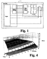
- Fig. 1 represents the modern state of the art in circuitry.
- the output currents are usually detected with current sensors (2).
- the instantaneous value of the current signal is compared with a threshold value that lies outside the normal operating range. If the threshold value is exceeded, the entire system, that is to say the circuit arrangement, is switched off.
- the threshold values are determined on the basis of thermal Measurements during the development and testing phase of each newly devised Systems of circuit arrangements.
- thermal Measurements during the development and testing phase of each newly devised Systems of circuit arrangements.
- (3) predictions for allowable loads that fixed that fixed
- the basis for the threshold values of all subsequently constructed arrangements are.
- the after 1 shows some disadvantages.
- the thresholds are static in nature, they have to be repeated for each individual Influencing factor can be determined and determined anew with every change. Any dynamic Changing the circuit arrangement, such as undervoltage in the ventilation system, Contamination of the cooling profiles or fluctuating ambient temperatures causes a Change in the readiness for performance of the circuit arrangement and must with static Threshold limitation are taken into account as a reserve.
- the constructive The performance of such a circuit arrangement cannot be fully utilized. In in any case, the most unfavorable working conditions for the borderline determinations serve, which means significant performance cuts.
- Hei-7-255166 is a circuit corresponding to the state of the art presented. Thermal overload protection is shown, which includes the power components of an inverter at low output frequency. For this, the time is determined after which would exceed the limit temperature of the power component for a given load. Before this time is reached, the converter is switched off if there is nothing wrong with the Load situation has changed.
- EP 0 792 008 A2 describes a method and a device for thermal Overload protection for converters with sinusoidal output variables, in which the Temperature rise of the component is evaluated when a defined one is exceeded Rise limit, the duty cycle is reduced to the thermal overload of the Avoid power component.
- Fig. 2 outlines an inventive example for the determination of transmission losses.
- the determination of the guide losses is explained using an example with IGBT structures from the current operating conditions. Because of the inertia of the heat transport, it is important to collect the data required for the overload protection directly at the point of origin, that is the basis of the inventive idea.
- the point of origin can be found in the pn junctions of the power transistors and diodes, consequently measured values and measurements must be carried out directly on these components.
- the “base leakage losses” are determined as a characteristic value for the power components used for standard operation and used for evaluation.
- the base transmission losses are defined by the electrical energy converted into heat, which arises in the transmission phase of the IGBT used as an example. Due to the design, this heat loss is functionally dependent on the amount of transported output current (I phase ), which is detected with a current sensor.
- the current lead time is related to the lead time of the component in standard operation (relative lead time).
- the detection and evaluation of the chip temperature ( ⁇ J ) as the current junction temperature of the semiconductor component is of crucial importance for a functional working of the overload protection.
- a factor from the current-dependent base leakage losses is found from the current junction temperature using a "correction factor temperature" (K ⁇ D).
- K ⁇ D correction factor temperature
- the chip temperature primarily increases depending on the size of the power loss generated.
- the chip temperature of a chip can also be increased passively by other components with power dissipation because they are positioned on the same thermally interconnected carriers.
- the heat sink temperature is the starting condition for the junction temperature for the following conditions, the respective in the previous one Calculated temperature used.
- the correction factor temperature (K ⁇ D) becomes determined via the characteristic curve relationship to the junction temperature.
- the frequency factor results from the clock frequency and the realized work cycle after evaluation via a correction factor (Kakt).
- Kakt the factor of the intermediate circuit voltage to (Uzk) results after evaluation via a correction factor (KU).
- KU correction factor
- the temperature correction factor (K ⁇ S) is determined from the current junction temperature for the current-independent base losses.
- the product of the multiplication point (X) in FIG. 3 forms the result "Switching losses / switches" as the second value calculated as an example.
- the current Switching losses of the semiconductor component are reflected.
- the sum of switching losses and routing losses per chip represent the total load of the respective semiconductor chips, these are fed to a thermal model of the semiconductor arrangement and the current chip temperature ( ⁇ J ) is determined from this.
- the current just possible output current and thus the degree of the current capacity utilization of the system can be determined, or the available reserve for the limit can be announced.
- the higher-level control can thus determine utilization trends and thus react in advance.
- This dynamic threshold shown here is the aim of the invention. Will the threshold namely designed self-adapting, then on the one hand without destroying the Circuit arrangement an overload shutdown, but it can be driven depending on the dynamic threshold, a reduced power can be impressed and an error message can appear in parallel.
- the present invention is not based on sinusoidal current profiles, the associated one Power factor and its adjustment, but from the current lead time of each individual component. This invention thus makes it application-independent Protection concept before that for all hard switching systems and thus among others also for Synchronous motors, brushless DC motors, power supplies and welding machines can be used is.
- the assignment of the protective device to the power section in the simplest case to one Switch with free-wheeling diode, to a half-bridge or an H-bridge is the basis for this independence.
- the temperature dependence of the components as well as the influence of the DC link voltage are largely taken into account for the operating variables described.
- the heat sink temperature is recorded as the basic variable for calculating the current chip temperature ( ⁇ J ).
- the current utilization is determined from the aforementioned current data and made available to the higher-level system as information. By reducing the load or frequency, the current thermal load can be reduced and switching off due to exceeding the temperature limits avoided.
- FIG. 5 outlines a subcircuit for inventive signal acquisition. The determination of the component lead time is explained using the example of a circuit section of an inventive circuit arrangement.
- the commutation circuit of an IGBT is shown in the TOP position and a freewheeling diode in the bottom position of a half-bridge.
- the positive output current flowing out of this circuit branch corresponds to a HIGH signal, if the drive signal has a HIGH level, then the IGBT is driven.
- either the bottom freewheeling diode or the TOP transistor be a leader.
- the polarity of the output current (iac) is therefore decisive for the Selection of TOP transistor and bottom freewheeling diode as currently active components. If the TOP transistor is activated at the same time with a positive output current, then the current flows through the transistor, the freewheeling diode is switched off.
- the & - combination of current polarity and TOP transistor control signal has at the output a HIGH signal, if the current is positive and the TOP transistor is driven, then this signal is characteristic of the "ON state" of the TOP transistor.
- a standardized signal provides information about a relative duty cycle of the TOP transistor.
- the & - combination of current polarity and inverted TOP transistor control signal has a HIGH signal at the output if the current is positive and the TOP transistor is controlled, then this signal is characteristic of the "ON state" of the Free-wheeling diode bottom. Compared to a standardized signal, information is obtained over a relative duty cycle of the free-wheeling diode Bottom.
- An electronic one Nameplate can be created. This enables digital data exchange with a controller are detailed error messages instead of summation error naming with a digital actual value output possible. Current actual time values for temperatures of the chips and heat sink as well resulting current limits are available.
Landscapes
- Inverter Devices (AREA)
- Power Conversion In General (AREA)
- Investigation Of Foundation Soil And Reinforcement Of Foundation Soil By Compacting Or Drainage (AREA)
- Control Of Eletrric Generators (AREA)
- Interface Circuits In Exchanges (AREA)
- Transmitters (AREA)
- Power Sources (AREA)
- Rectifiers (AREA)
Abstract
Description
Die Erfindung beschreibt eine Schaltungsanordnung für Stromumrichter nach den Merkmalen
des Oberbegriffes des Anspruches 1. Derartige Schaltungsanordnungen sind beispielhaft
bekannt aus M. Faschin "On-Line Monitoring of Chip Temperature in IGBT Inverters for
Propulsion Systems" in EPE Journal Vol. 5 No. 1 March 1995. Die Problematik der
zuverlässigen und zerstörungsfreien Arbeit der Schaltungsanordnungen gewinnt bei der
weiteren Erhöhung ihrer Leistungsdichte zunehmend an Bedeutung.The invention describes a circuit arrangement for power converters according to the features
of the preamble of
Bei Einsatz von Transistorschaltern aus neuester Entwicklung, wie sie in der Technologie von IGBT und MOSFET dargestellt werden und dem Einsatz von modernen Freilaufdioden mit soft- recovery- Verhalten nach Technologien, wie sie in DE 44 21 529 A1 vorgestellt wurden, können die verschiedensten konventionellen Fehler zur Beeinflussung der Ansteuerung und damit zu Fehlsteuerungen führen, was seinerseits zum Ausfall der Schaltungsanordnung führen kann, oder schwerwiegende negative Folgen in der Arbeitsweise nach sich zieht. When using transistor switches from the latest development, such as in the technology of IGBT and MOSFET are shown and the use of modern freewheeling diodes soft recovery behavior according to technologies as presented in DE 44 21 529 A1, can use a variety of conventional errors to influence the control and thus lead to incorrect controls, which in turn lead to failure of the circuit arrangement can, or have serious negative consequences for the way you work.
Bei hoher Packungsdichte, also sehr kompaktem Aufbau beeinflußt das Magnetfeld der Hauptstromführungen bei eng benachbarten Hauptstrom- und Ansteuerverbindungen die Funktionssicherheit, insbesondere bei Leistungsschaltern mit hoher Schaltgeschwindigkeit und großen Werten von di/dt (schnelle Schalter), weil sich jede einzelne Leitungsverbindung als Störimpuls beim Schaltbetrieb verhalten kann, was in der Ansteuerung besonders kritisch ist und deshalb besondere Schutzmaßnahmen erfordert, wie das bereits in DE 196 28 131 A1 dargestellt wurde.With a high packing density, i.e. a very compact design, the magnetic field of the main current guides with closely adjacent main current and control connections influences the functional reliability, especially in circuit breakers with high switching speeds and large values of di / dt (fast switches), because each individual line connection is a disturbance pulse during switching operation can behave, which is particularly critical in the control and therefore requires special protective measures, as has already been described in DE 196 28 131 A1.
Zumindest wird die mögliche Höchstleistung von Schaltungsanordnungen dadurch gemindert, daß nicht alle Faktoren möglicher Störungen der bei dem Betrieb von Schaltungsanordnungen auftretenden Schwankungen einzelner Parameter konstruktiv so berücksichtigt werden können, wie sie bei dem praktischen Betrieb auftreten können. Es sind für real mögliche negative Parameteränderungen Reserven der Belastbarkeit konstruktiv in der Anordnung einzubauen, die objektiv nicht sinnvoll sind, aber die die Verlustleistungen negativ beeinflussen.At least the possible maximum performance of circuit arrangements is reduced by that not all factors of possible interference in the operation of circuit arrangements occurring fluctuations of individual parameters can be taken into account constructively, as they can occur in practical operation. It is for real possible negative Parameter changes to incorporate reserves of the load-bearing capacity in the arrangement, which are not objectively sensible, but which have a negative impact on the power losses.
Die Spannweite aller möglichen Störungen ist sehr groß, hier möge nur ein Teil der beeinflussenden Kenngrößen aufgezählt werden, um die Komplexität dieser Erfindung darzustellen:
- Die Betriebssicherheit der Leistungsschalter selbst wird durch seine dynamischen Parameter, deren kenndatenbedingten Schwankungsbreite und des dadurch verursachten unterschiedlichen Temperaturverhaltens bestimmt.
- Die zur Kommutierung eingesetzte Freilaufdiode stimmt nicht völlig in ihrem Verhalten mit dem Leistungsschalter überein.
- Die DCB- Keramik als direkter Träger der eben genannten aktiven mit pn- Übergängen versehenen Leistungsbauelemente besitzt nicht genau die gleiche Geometrie in der Wiederholung bei Parallelschaltungen in einer Schaltungsanordnung.
- Es sind unterschiedlich große Kupferflächen durch das Strukturbild und der Toleranzen in der Ätztechnik für Kupfer vorhanden, dadurch bedingt sind unterschiedliche Kapazitätswerte begründet, die in unterschiedlichem Maße parasitäre Induktivitäten darstellen.
- The operational safety of the circuit breaker itself is determined by its dynamic parameters, their fluctuation range based on the characteristic data and the resulting different temperature behavior.
- The behavior of the freewheeling diode used for commutation does not completely match the behavior of the circuit breaker.
- The DCB ceramic as the direct carrier of the active power components just mentioned provided with pn junctions does not have exactly the same geometry in the repetition in the case of parallel connections in a circuit arrangement.
- There are copper surfaces of different sizes due to the structure and the tolerances in the etching technology for copper.
Ein induktivitätsarmer Aufbau wird bereits in der kleinsten Zelle angestrebt, Unterschiede sind praktisch immer vorhanden. Diese Problematik ist beispielhaft Gegenstand der Erfindung in DE 41 05 155 A1.A low-inductance design is sought in the smallest cell, there are differences practically always present. This problem is exemplarily the subject of the invention in DE 41 05 155 A1.
Wie Erprobungen gezeigt haben, sind wesentliche Gesichtspunkte zur Reduzierung von parasitären Induktivitäten auch in der äußeren Verschaltung der Schaltungsanordnung beachtlich. Möglichkeiten zur Verringerung solcher Induktivität ergeben sich erfindungsgemäß nach DE 42 40 501 A1 dadurch, daß der positive und der negative Stromanschluß für die Schaltungsanordnung nicht nur eng beieinander liegen, sondern aus mehreren Teilanschlüssen gebildet werden, die ihrerseits möglichst symmetrisch an die einzelnen Schalter heranzuführen sind.As tests have shown, essential considerations for the reduction of Parasitic inductances also in the external circuitry of the circuit arrangement considerable. Possibilities for reducing such inductance arise according to the invention according to DE 42 40 501 A1 in that the positive and the negative power connection for the Circuit arrangement not only lie close together, but from several sub-connections are formed, which in turn lead to the individual switches as symmetrically as possible are.
Die Streuinduktivität bei Parallel- und Zusammenschaltung mehrerer Kommutierungskreise gewinnt zunehmend an Bedeutung. Bei Parallelschaltungen treten weiterhin unterschiedliche Weglängen der Gleichstrom führenden Stromzweige auf, was zu nicht gewollten veränderten Ansteuerungen der Leistungsschalter führt. Dieser Problematik widmet sich DE 19519538 A1.The leakage inductance when several commutation circuits are connected and connected in parallel is becoming increasingly important. Different connections continue to occur in parallel connections Path lengths of the current branches leading to direct current, which changed to unwanted ones Controls of the circuit breaker leads. DE 19519538 A1 addresses this problem.
Ein weiteres Feld der Toleranzen mit möglichen negativen Wirkungen eröffnet sich bei der Betrachtung der eingesetzten Kühlsysteme. Nicht jede zu kühlende DCB- Keramik kann an einem gleichbegünstigten Ort von einem Kühlkörper auf immer gleicher Temperatur gehalten werden. Die Kühlleistungen an sich sind darüber hinaus in jedem Falle dynamisch zu sehen, denn die abzuführende Verlustleistung kann in Größenordnungen an einzelnen Stellen der DCB- Keramik unterschiedlich sein. Sich verändernde Wärmegradienten des Kühlkörpers können sich darüber hinaus neben all den sich durch äußere Einflüsse ergebenden Faktoren erst im Verlaufe des Betreibens von Schaltungsanordnungen einstellen. Another field of tolerances with possible negative effects opens up at Consideration of the cooling systems used. Not every DCB ceramic to be cooled can kept in a favored location by a heat sink at the same temperature become. The cooling capacities themselves can also be seen dynamically in any case, because the power loss to be dissipated can be of the order of magnitude at individual points DCB ceramics may be different. Changing heat gradients of the heat sink in addition to all the factors resulting from external influences adjust in the course of operating circuit arrangements.
Unterschiedliche Taktfrequenzen, Phasenverschiebungen zwischen aktiver Leistung und Scheinleistung, die Grundfrequenz des Schaltungsausganges und die Zwischenkreisspannungen sind weitere qualitativ genannte Parameter, die zu einer nicht zu überschauenden Vielzahl von Einflußfaktoren gehören, von deren Größe Auswirkungen auf die Funktionssicherheit und Belastbarkeit einer jeden Schaltungsanordnung zu erwarten sind. Nicht alle diese Parameter können konstruktiv so berücksichtigt werden, daß mit einer minimierten Schaltungsreserve ein Konzept verwirklicht werden kann, es sind immer Leistungsabstriche in der Konstruktion von Schaltungsanordnungen zu machen.Different clock frequencies, phase shifts between active power and Apparent power, the basic frequency of the circuit output and the intermediate circuit voltages are other qualitatively named parameters that lead to a multitude of Influencing factors include, the size of which affects the functional safety and Resilience of each circuit arrangement can be expected. Not all of these parameters can be considered constructively so that with a minimized circuit reserve Concept can be realized, there are always performance cuts in the construction of To make circuit arrangements.
Zum Schutz der Schaltungsanordnungen vor negativ auf die Funktionsfähigkeiten wirkender Überlastungen sind neben der Absenkung der vorgeschriebenen maximalen Leistungsfähigkeit Veröffentlichungen bekannt, die Methoden der Früherkennung zerstörerisch wirkender Effekte aufzeigen. Dazu werden die folgenden Erfindungen genannt:To protect the circuit arrangements against negative effects on the functional capabilities Overloads are in addition to lowering the prescribed maximum performance Publications known the methods of early detection of destructive effects show. The following inventions are mentioned:
In DE 43 19 254 A1 wird eine Leistungshalbleiterschaltungsanordnung vorgestellt, die zum Schutz vor Überströmen, also auch vor Kurzschlußströmen, vorgesehen wird. Der Überstrom wird hier mittels Stromsensoren erfaßt, die über Fensterkomperatoren, Fehlerspeicher und Einschaltsperren die Schaltungsanordnung durch Abschalten vor Zerstörung schützt.In DE 43 19 254 A1 a power semiconductor circuit arrangement is presented, which for Protection against overcurrents, including short-circuit currents, is provided. The overcurrent is detected here by means of current sensors, which are via window comparators, fault memories and Power-on locks protect the circuitry from being destroyed by switching it off.
DE 44 10 978 A1 beschreibt ein Verfahren und eine dazugehörige Schaltung zur Verbesserung der Kurzschlußfestigkeit eines bipolaren MOS- Transistors. Die in dieser Schaltungsanordnung zur Realisierung der Gate- Spannungsfestigkeit eingesetzten Zenerdioden begrenzen die Spannung zwischen dem MOSFET und der Gate- Elektrode des IGBT.DE 44 10 978 A1 describes a method and an associated circuit for improvement the short-circuit strength of a bipolar MOS transistor. The in this circuit arrangement Zener diodes used to realize the gate dielectric strength limit the Voltage between the MOSFET and the gate electrode of the IGBT.
Der Problematik des Kurzschlusses in Stromrichtern mit IGBT oder MOSFET ist in der Literatur nach dem Stand der Technik viel Platz eingeräumt. EP 0 190 925 A1 stellt diese Problematik vor, hier wird die maximal zulässige Durchlaßspannung (Vce) eines IGBT unter Voraussetzung eines maximal erlaubten Kollektorstromes von der Höhe der Gatespannung Vge in Abhängigkeit gebracht, also eine Begrenzung der höchstmöglichen Leistung diktiert. The problem of short circuits in converters with IGBT or MOSFET is in the Prior art literature has given plenty of space. EP 0 190 925 A1 provides this Problem, here the maximum permissible forward voltage (Vce) of an IGBT is below Prerequisite for a maximum permitted collector current from the level of the gate voltage Vge brought into dependence, that is, a limitation of the highest possible performance dictated.
Die dem Stand der Technik zuordenbaren Maßnahmen zur Erhöhung der Leistungsdichte in den Schaltungsanordnungen beinhalten Maßnahmen zur Verwendung geeigneter paralleler Kupferplatten als Stromschienen, Minimieren der stromdurchflossenen Flächen, Minimieren der Isolationsschichtdicke bei eng benachbarten Platten der gegensätzlichen Pole, Parallelschalten von parasitären Induktivitäten und Zusammenfassen der gleichpoligen Schienen über kurze Wege bei großem Leitungsquerschnitt.The measures which can be assigned to the prior art for increasing the power density in the circuit arrangements contain measures for the use of suitable parallel Copper plates as busbars, minimizing the areas through which current flows, minimizing the insulation layer thickness in the case of closely adjacent plates of the opposite poles, Connecting parasitic inductances in parallel and combining the same-pole Rails over short distances with a large cable cross-section.
In jüngerer Zeit wird der Einsatz von Sensoren zur Erfassung und Bewertung verschiedener Parameter der Umrichteranordnungen im Echtzeitverhalten beschrieben. Strom- und Temperatursensoren sind zwischenzeitlich fester Bestandteil des Aufbaus von Schaltungsanordnungen der Leistungsklasse, insbesondere zum Erzielen hoher Zuverlässigkeit. Die Augenblickssignale werden mit Schwellwerten verglichen, bei dessen Überschreitung wird das gesamte System abgeschaltet und damit vor Zerstörung bewahrt.More recently, the use of sensors to detect and evaluate various Parameters of the converter arrangements described in real time behavior. Electricity and In the meantime, temperature sensors have become an integral part of the construction of Circuit arrangements of the performance class, in particular to achieve high reliability. The instantaneous signals are compared with threshold values, which are exceeded when exceeded the entire system is switched off and thus protected from destruction.
Die Festlegung der Schwellwertgrenzen erfolgt nach dem Stand der Technik in der Konzeptphase der Entwicklung der Schaltungsanordnung, es ist ein festgeschriebener Wert, der statisch aufgeprägt ist. Bei Veränderungen des Systems in einem Teilbereich, wie beispielhaft bei Einsatz eines anderen Kühlkörpers, muß der Schwellwert separat neu festgestellt und eingeprägt werden. Nicht alle Veränderungen von Teilbereichen einer Schaltungsanordnung können prophylaktisch bewertet werden, wodurch die Gefahr für ein unkontrolliertes partielles Übersteigen zulässiger Arbeitsbereiche möglich und auf längere Sicht unvermeidlich ist.The threshold values are determined according to the state of the art in the Concept phase of the development of the circuit arrangement, it is a fixed value, which is statically imprinted. If the system changes in a sub-area, such as as an example when using a different heat sink, the threshold value must be new separately determined and impressed. Not all changes in parts of one Circuitry can be assessed prophylactically, reducing the risk of an uncontrolled partial exceeding of permissible work areas possible and in the long term is inevitable.
Die vorliegende Erfindung hat die Aufgabe, eine Schaltungsanordnung mit einer Erfassung aller aktuell relevanten Betriebsbedingungen als Parameter vorzustellen, die aus diesen permanent vorhandenen Werten eine selbstadaptierende Stromabschaltschwelle generiert, die unabhängig vom überlagerten Regelsystem arbeitet, so daß eine dynamische Echtzeitbewertung des Leistungsparameter- Kennfeldes erfolgt und somit ausschließlich aktuell normierte Daten über die Auslastung und Belastbarkeit in Form einer kennfeldorientierten Überlastbewertung an das überlagerte Regelsystem des Controllers geliefert werden. The present invention has the task of a circuit arrangement with a detection to present all currently relevant operating conditions as parameters, based on these permanently existing values generates a self-adapting power cut-off threshold that works independently of the higher-level control system, so that a dynamic real-time evaluation of the performance parameter map and thus only currently standardized data about utilization and resilience in the form of a map-oriented overload assessment be delivered to the higher-level control system of the controller.
Die Aufgabe wird bei Schaltungsanordnungen der dargestellten Art durch die Maßnahmen des
kennzeichnenden Teiles des Anspruches 1 gelöst, bevorzugte Weiterbildungen werden in den
Unteransprüchen aufgezeigt.The task is in circuit arrangements of the type shown by the measures of
characterizing part of
Das Generieren einer sich selbst adaptierenden Stromabschaltschwelle setzt einerseits das Erfassen und Uniformieren aller signifikanten Parameter aus dem Leistungsteil einer Schaltungsanordnung über Sensoren bzw. elektrische Abzweigungen und andererseits deren Verarbeitung und Bewertung in einer extra zu diesem Zweck eingebauten Ansteuer- und Schutzschaltung voraus.On the one hand, generating a self-adapting current cut-off threshold sets this Acquisition and uniformization of all significant parameters from the power section of a Circuit arrangement via sensors or electrical branches and, on the other hand, their Processing and evaluation in a control and built-in for this purpose Protection circuit ahead.
Erfindungsgemäß wird innerhalb des Leistungsteiles der Schaltungsanordnung aus den Parametern ein mehrdimensionales Kennfeld gebildet, in dem deren Bewertung auf der Grundlage ihrer Auswirkungen auf die Temperaturerhöhung des Gesamtsystems der Schaltungsanordnung erfolgt.According to the invention within the power section of the circuit arrangement Parameters, a multi-dimensional map is formed in which their evaluation on the Basis of their effects on the temperature increase of the overall system of Circuit arrangement takes place.
Bedingt durch die hier dargestellten Prämissen ist es sehr vorteilhaft, die erfinderische Schutzschaltung direkt auf dem Leistungsteil der Anordnung zu positionieren, das hat den weiteren Vorteil, daß die Weiterleitung der autark erfaßten Umgebungsbedingungen der zu schützenden Leistungsschalter nicht nur zur Bildung eines dynamischen Abschaltkriteriums herangezogen, sondern in Echtzeit einem übergeordneten Controllersystem zur Auswertung zur Verfügung gestellt wird.Due to the premises presented here, it is very advantageous to the inventive Positioning the protective circuit directly on the power section of the arrangement has that Another advantage is that the forwarding of the autonomously recorded environmental conditions protective circuit breakers not only to form a dynamic disconnection criterion used, but in real time a higher-level controller system for evaluation is made available.
Die Schutzschaltung basiert auf den Eigenschaften der eingesetzten Leistungsschalter, die durch ihre konstruktiv bedingten Schaltverluste, deren Durchlaßverluste und inneren thermischen Widerstände die Grundlage für die Dimensionierung eines Betriebskennfeldes bilden.The protective circuit is based on the properties of the circuit breakers used through their design-related switching losses, their transmission losses and internal thermal resistances are the basis for dimensioning an operating map form.
Beispielhaft sind Betriebsparameter wie Temperatur des Kühlkörpers, Taktfrequenz, Zwischenkreisspannung, zeitlicher Leitzustand von IGBT bzw. Freilaufdiode signifikante und meßbare Parameter. Sie sind für jeden Leistungsschalter bekannte und definierte Größen, die in den Grenzen des dynamischen Verhaltens im Einsatz variieren, bzw. konstant sind. Diese Betriebsparameter bilden beispielhaft das Kennfeld, das durch seine korrelative Bewertung zu den jeweils augenblicklich zulässigen Schwellwertergebnissen führt. Diese Schwellwerte begrenzen autark die maximal mögliche Belastung zu diesem Zeitpunkt.Operating parameters such as temperature of the heat sink, clock frequency, DC link voltage, leading time status of IGBT or freewheeling diode significant and measurable parameters. They are known and defined sizes for each circuit breaker the limits of dynamic behavior in use vary or are constant. This Operating parameters form an example of the map, which is due to its correlative evaluation leads to the currently permissible threshold results. These threshold values limit the maximum possible load at this time.
Der Schutz des Leistungsteiles jeder Schaltungsanordnung kann durch die erfinderischen Maßnahmen über ein definiertes Kennfeld durch Bewertung der zu jeder Zeit vorhandenen Arbeitstemperatur und der Taktfrequenz des Systems erreicht werden. Unabhängig von äußeren Bedingungen wird die Einhaltung der vorgegebenen Grenzwerte und die Zulässigkeit jedes vom Controller angestrebten Zustandes überprüft.The protection of the power section of each circuit arrangement can be achieved by the inventive Measures over a defined map by evaluating the available at any time Working temperature and the clock frequency of the system can be achieved. Independent of external conditions becomes compliance with the specified limit values and the admissibility checks every state desired by the controller.
Bei aktuellen Anlässen kann in gleicher Weise ein Eingrenzen des aktuell zulässigen Stromwertes erfolgen und damit eine Fahrweise mit verminderter Leistung oder veränderter Taktfrequenz gewählt werden, um durch eine momentane verminderte Stromtragfähigkeit als Ergebnis der Bewertung des Kennfeldes ein Abschalten der gesamten Schaltungsanordnung überflüssig zu machen oder zeitlich zu strecken.On current occasions, the currently permissible can be narrowed down in the same way Current values take place and thus a driving style with reduced performance or changed Clock frequency can be chosen to be reduced by a momentary current carrying capacity Result of the evaluation of the map, switching off the entire To make circuitry redundant or to stretch over time.
In die Kennfeldbewertung können weitere Einflußgrößen des Arbeitsbereiches der Schaltungsanordnung aufgenommen werden, so ist es beispielhaft möglich, den aktuellen Stand der Zwischenkreisspannung zusätzlich zu berücksichtigen und eine Bewertung der Stromflußzeit ist erreichbar.Other influencing variables of the work area of the Circuit arrangement are included, so it is possible, for example, the current status the DC link voltage must also be taken into account and an evaluation of the Current flow time is achievable.
Zusammenfassend gilt die Aussage, daß auf der Grundlage eines installierten komplexen Kennfeldes eine dem aktuellen Zustand der Schaltungsunordnung adäquate Strombegrenzung möglich ist und es ist durch eine interne analoge Signalverarbeitung im Kennfeld eine sehr geringe Verzögerungszeit von kleiner als 1 ms möglich. Durch einen D/A- Wandler in Zusammenwirken mit einem Mikroprozessor oder Signalprozessor stehen die gewonnenen Kennfeldinformationen auch für digitale Schnittstellen zur Verfügung. In summary, the statement is that on the basis of an installed complex A current limitation adequate to the current state of the circuit disorder is possible and it is very much due to an internal analog signal processing in the map short delay time of less than 1 ms possible. Through a D / A converter in Interaction with a microprocessor or signal processor is the result Map information is also available for digital interfaces.
Nachfolgend werden die Erfindungsgedanken an Hand von skizzenhaften Darstellungen in den
Figuren 1 bis 5 näher erläutert:
Fig. 1 stellt den modernen Stand der Schaltungstechnik dar. In Umrichtern (1) werden die Ausgangsströme in der Regel mit Stromsensoren (2) erfaßt. Zum Schutz vor Überlastung wird der Augenblickswert des Stromsignals mit einem Schwellwert, der außerhalb des normalen Betriebsbereiches liegt, verglichen. Bei Überschreiten des Schwellwertes wird das Gesamtsystem, also die Schaltungsanordnung, abgeschaltet. Fig. 1 represents the modern state of the art in circuitry. In converters (1), the output currents are usually detected with current sensors (2). To protect against overload, the instantaneous value of the current signal is compared with a threshold value that lies outside the normal operating range. If the threshold value is exceeded, the entire system, that is to say the circuit arrangement, is switched off.
Die Festlegung der Schwellwerte erfolgt bei derartigen Systemen aufgrund thermischer Messungen während der Entwicklungs- und Erprobungsphase eines jeden neu erdachten Systems von Schaltungsanordnungen. In Erweiterung dieser Vorgehensweise werden für bestimmte Kühlkörpertemperaturen (3) Vorhersagen für erlaubte Belastungen fixiert, die Grundlage für die Schwellwerte aller nachträglich aufgebauten Anordnungen sind. Der nach Fig. 1 aufgezeigte Stand der Technik birgt in sich einige Nachteile. Bei Änderungen der Schaltungsanordnungen im Bereich des Leistungsteiles, beispielhaft bei Einsatz eines anderen Kühlkörpers, müssen die Schwellwerte durch erneute thermische Messungen neu definiert werden. In such systems, the threshold values are determined on the basis of thermal Measurements during the development and testing phase of each newly devised Systems of circuit arrangements. In expanding this approach, for certain heatsink temperatures (3) predictions for allowable loads that fixed The basis for the threshold values of all subsequently constructed arrangements are. The after 1 shows some disadvantages. When the Circuit arrangements in the area of the power section, for example when using another Heatsink, the threshold values have to be redefined by renewed thermal measurements become.
Die Schwellen sind statischer Natur, sie müssen immer wieder für jeden einzelnen Einflußfaktor bei jeder Änderung neu ermittelt und festgelegt werden. Jede dynamische Veränderung der Schaltungsanordnung, wie beispielhaft Unterspannungen am Lüftungssystem, Verschmutzung der Kühlprofile oder schwankende Umgebungstemperaturen bewirkt eine Änderung der Leistungsbereitschaft der Schaltungsanordnung und muß bei statischer Schwellwertbegrenzung als Reserve berücksichtigt werden. Die konstruktive Leistungsfähigkeit einer solchen Schaltungsanordnung kann nicht voll genutzt werden. In jedem Falle müssen die ungünstigsten Arbeitsbedingungen für die Grenzfallfestlegungen dienen, was erhebliche Leistungsabstriche bedeutet.The thresholds are static in nature, they have to be repeated for each individual Influencing factor can be determined and determined anew with every change. Any dynamic Changing the circuit arrangement, such as undervoltage in the ventilation system, Contamination of the cooling profiles or fluctuating ambient temperatures causes a Change in the readiness for performance of the circuit arrangement and must with static Threshold limitation are taken into account as a reserve. The constructive The performance of such a circuit arrangement cannot be fully utilized. In in any case, the most unfavorable working conditions for the borderline determinations serve, which means significant performance cuts.
In Hei-7-255166 wird eine dem Stand der modernen Technik entsprechende Schaltung vorgestellt. Es wird ein thermischer Überlastschutz dargestellt, der die Leistungsbauelemte eines Umrichters bei niedriger Ausgangsfrequenz schützt. Hierzu wird die Zeit bestimmt, nach der die Grenztemperatur des Leistungsbauelementes bei gegebener Last überschritten würde. Vor Erreichen dieser Zeit wird der Umrichter abgeschaltet, wenn sich nichts an der Belastungssituation geändert hat.In Hei-7-255166 is a circuit corresponding to the state of the art presented. Thermal overload protection is shown, which includes the power components of an inverter at low output frequency. For this, the time is determined after which would exceed the limit temperature of the power component for a given load. Before this time is reached, the converter is switched off if there is nothing wrong with the Load situation has changed.
EP 0 792 008 A2 beschreibt eine Methode und eine Vorrichtung für den thermischen Überlastschutz bei Umrichtern mit sinusförmigen Ausgangsgrößen, bei dem der Temperaturanstieg des Bauelementes ausgewertet wird, bei Überschreiten einer definierten Anstiegsgrenze wird das Tastverhältnis reduziert, um die thermische Überlastung des Leistungsbauelementes zu vermeiden.EP 0 792 008 A2 describes a method and a device for thermal Overload protection for converters with sinusoidal output variables, in which the Temperature rise of the component is evaluated when a defined one is exceeded Rise limit, the duty cycle is reduced to the thermal overload of the Avoid power component.
Fig. 2 skizziert ein erfinderisches Beispiel für die Bestimmung von Durchlaßverlusten. Die Ermittlung der Leitverluste wird an einem Beispiel mit IGBT- Aufbauten aus den aktuellen Betriebsbedingungen erläutert. Wegen der Trägheit des Wärmetransportes ist es wichtig, die für den Überlastschutz erforderlichen Daten direkt an der Entstehungsstelle zu erheben, das ist Grundlage der erfinderischen Idee. Die Entstehungsstelle ist in den pn- Übergängen der Leistungstransistoren und -dioden zu finden, folglich müssen Meßwerte und Messungen unmittelbar an diesen Bauelementen erfolgen. Fig. 2 outlines an inventive example for the determination of transmission losses. The determination of the guide losses is explained using an example with IGBT structures from the current operating conditions. Because of the inertia of the heat transport, it is important to collect the data required for the overload protection directly at the point of origin, that is the basis of the inventive idea. The point of origin can be found in the pn junctions of the power transistors and diodes, consequently measured values and measurements must be carried out directly on these components.
So werden in Abhängigkeit von dem Ausgangsstrom die "Basisdurchlaßverluste" als Kennwert für die eingesetzten Leistungsbauelemente für den Normbetrieb ermittelt und zur Bewertung herangezogen. Die Basisdurchlaßverluste werden durch die in Wärme umgewandelte elektrische Energie definiert, die in der Durchlaßphase des beispielhaft eingesetzten IGBT entstehen. Konstruktionsbedingt ist diese Verlustwärme funktionell von der Menge des transportierten Ausgangsstromes (Iphase), der mit einem Stromsensor erfaßt wird, abhängig.Depending on the output current, the "base leakage losses" are determined as a characteristic value for the power components used for standard operation and used for evaluation. The base transmission losses are defined by the electrical energy converted into heat, which arises in the transmission phase of the IGBT used as an example. Due to the design, this heat loss is functionally dependent on the amount of transported output current (I phase ), which is detected with a current sensor.
Die Einschaltdauer als "relative Leitdauer", die den Zeitraum des beispielhaft verwendeten IGBT einer Schaltperiode umfaßt, ist ein zweiter signifikanter Schaltparameter und Faktor für die Steuerung der zulässigen Belastbarkeit der Schaltungsanordnung. Für den Korrekturfaktor Leitdauer (KLD) wird die aktuelle Leitdauer auf die Leitdauer des Bauelementes im Normbetrieb bezogen (rel. Leitdauer).The duty cycle as "relative lead time", which includes the period of the exemplary IGBT of a switching period, is a second significant switching parameter and factor for controlling the permissible load capacity of the circuit arrangement. For the correction factor lead time (K LD ), the current lead time is related to the lead time of the component in standard operation (relative lead time).
Die Erfassung und Bewertung der Chiptemperatur (ϑJ) als aktuelle Sperrschichttemperatur des Halbleiterbauelementes ist für ein funktionstüchtiges Arbeiten des Überlastschutzes von entscheidender Bedeutung. Über einen "Korrekturfaktor Temperatur" (KϑD) wird aus der aktuellen Sperrschichttemperatur ein Faktor aus den stromabhängigen Basisdurchlaßverlusten gefunden. Einerseits erhöht sich primär die Chiptemperatur in Abhängigkeit von der Größe der erzeugten Verlustleistung. Andererseits kann die Chiptemperatur eines Chips auch passiv durch andere Bauelemente mit Verlustleistung dadurch erhöht werden, weil sie auf gleichen thermisch miteinander verbundenen Trägern positioniert sind.The detection and evaluation of the chip temperature (ϑ J ) as the current junction temperature of the semiconductor component is of crucial importance for a functional working of the overload protection. A factor from the current-dependent base leakage losses is found from the current junction temperature using a "correction factor temperature" (KϑD). On the one hand, the chip temperature primarily increases depending on the size of the power loss generated. On the other hand, the chip temperature of a chip can also be increased passively by other components with power dissipation because they are positioned on the same thermally interconnected carriers.
Es wird ganz allgemein indirekt durch die Schaltunganordnung mit deren übrigen Schaltelementen und/oder durch den Kühlkörper Wärme ausgleichend auf alle Bauteile übertragen und damit jeder einzelne Chip eine passive Wärmebelastung erhalten, zumindest jedoch erfolgt eine Beeinflussung. So ist es denkbar, daß unter ungünstigen Bedingungen kaum eine Leistung von einem Leistungsschalter erwartet werden kann, wenn die passive Erwärmung durch dessen "Umfeld" bereits sehr hoch ist. It is generally indirect through the circuit arrangement with its rest Switching elements and / or heat-compensating heat on all components transmitted and thus each individual chip receive a passive heat load, at least however, there is an influence. So it is conceivable that under unfavorable conditions hardly a power from a circuit breaker can be expected if the passive Warming due to its "environment" is already very high.
Als Startbedingung für die Sperrschichttemperatur wird die Kühlkörpertemperatur herangezogen, für die folgenden Bedingungen wird die jeweilige in der vorangegangenen Berechnung ermittelte Temperatur eingesetzt. Der Korrekturfaktor Temperatur (KϑD) wird über den Kennlinienzusammenhang zur Sperrschichttemperatur ermittelt.The heat sink temperature is the starting condition for the junction temperature for the following conditions, the respective in the previous one Calculated temperature used. The correction factor temperature (KϑD) becomes determined via the characteristic curve relationship to the junction temperature.
Diese hier beispielhaft dargestellten drei Parameter werden als Faktoren miteinander als Produkt über die Multiplikationsstelle zur weiteren Verwertung als nutzbarer Faktor "Durchlaßverluste/Schalter" der digitalen Bewertungseinheit (z.B. µ- Controller) zugeführt.These three parameters, which are shown here by way of example, are referred to as factors Product via the multiplication point for further utilization as a usable factor "Passage losses / switches" fed to the digital evaluation unit (e.g. µ-controller).
Fig. 3 skizziert ein Beispiel für die Bestimmung von Schaltverlusten. Aus den aktuellen Betriebsbedingungen am Beispiel eines IGBT werden die Daten ermittelt. Es werden vier Faktoren dargestellt. 3 outlines an example for the determination of switching losses. The data are determined from the current operating conditions using the example of an IGBT. Four factors are presented.
Aus dem Ausgangsstrom (Iphase) werden Basisschaltverluste als Kennwert der eingesetzten Leistungshalbleiterbauelemente fiir einen Normbetrieb ermittelt, in Abhängigkeit von dem Phasenstrom ergibt sich der erste Faktor fiir die nachfolgende Bewertung.Basic switching losses are determined from the output current (I phase ) as a characteristic value of the power semiconductor components used for standard operation, and the first factor for the subsequent evaluation is obtained as a function of the phase current.
Aus der Taktfrequenz und dem realisierten Arbeitstakt ergibt sich nach Bewertung über einen Korrekturfaktor (Ktakt) der Frequenzfaktor. In gleicher Weise ergibt sich nach Bewertung über einen Korrekturfaktor (KU) der Faktor der Zwischenkreisspannung auf (Uzk). In analoger Weise zu Fig. 2 wird der vierte Rechenwert, die Chiptemperatur (ϑJ), gebildet, hier jedoch mit den Schaltverlusten verknüpft. Es ergibt sich auch hier ein Temperaturfaktor. Der Korrekturfaktor Temperatur (KϑS) wird aus der aktuellen Sperrschichttemperatur für die stromunabhängigen Basisverluste ermittelt.The frequency factor results from the clock frequency and the realized work cycle after evaluation via a correction factor (Kakt). In the same way, the factor of the intermediate circuit voltage to (Uzk) results after evaluation via a correction factor (KU). The fourth calculation value, the chip temperature (ϑ J ), is formed in an analogous manner to FIG. 2, but here is linked to the switching losses. There is also a temperature factor here. The temperature correction factor (KϑS) is determined from the current junction temperature for the current-independent base losses.
Das Produkt der Multiplikationsstelle (X) in Fig. 3 bildet als Ergebnis die "Schaltverluste/Schalter" als zweiten beispielhaft errechneten Wert. Die aktuellen Schaltverluste des Halbleiterbauelementes werden widergespiegelt. The product of the multiplication point (X) in FIG. 3 forms the result "Switching losses / switches" as the second value calculated as an example. The current Switching losses of the semiconductor component are reflected.
Die Summe aus Schaltverlusten und Leitverlusten pro Chip (IGBT und Freilaufdiode) stellen die Gesamtbelastung der jeweiligen Halbleiterchips dar, diese werden einem thermischen Modell der Halbleiteranordnung zugeführt und daraus wird die aktuelle Chiptemperatur (ϑJ) ermittelt.The sum of switching losses and routing losses per chip (IGBT and free-wheeling diode) represent the total load of the respective semiconductor chips, these are fed to a thermal model of the semiconductor arrangement and the current chip temperature (ϑ J ) is determined from this.
Aus der Differenz der aktuellen Chiptemperatur (ϑJ) zur Chip- Grenztemperatur kann der aktuelle gerade noch mögliche Ausgangsstrom und damit der Grad der aktuellen Auslastbarkeit des Systems bestimmt werden, bzw. es kann die zur Verfügung stehende Reserve zur Grenze bekanntgegeben werden. Die überlagerte Steuerung kann damit Auslastungstendenzen bestimmen und so im Vorfeld reagieren.From the difference between the current chip temperature (ϑ J ) and the chip limit temperature, the current just possible output current and thus the degree of the current capacity utilization of the system can be determined, or the available reserve for the limit can be announced. The higher-level control can thus determine utilization trends and thus react in advance.
Fig. 4 skizziert ein erfindungsgemäßes dreidimensionales Kennfeld mit zwei Eingangssignalen, der Temperatur und der Arbeitsfrequenz. Die komplexe Wirkung von nur zwei Variablen zeigt die enormen Auswirkungen auf die Strombelastbarkeit. Bereits bei sehr guter Kühlung, also Temperaturen unter 50°C sinkt die Belastbarkeit bei 20 kHz auf etwa die Hälfte, bei nicht ausreichender Kühlleistung reduziert sich diese jedoch auf ein Viertel des eben genannten Wertes. 4 outlines a three-dimensional map according to the invention with two input signals, the temperature and the working frequency. The complex effect of just two variables shows the enormous impact on the current carrying capacity. Even with very good cooling, i.e. temperatures below 50 ° C, the load capacity at 20 kHz drops to about half, but if the cooling capacity is insufficient, this is reduced to a quarter of the value just mentioned.
In einem praktischen Fall wird jedoch ein vielfaches von Variablen wirksam, das gesamte Kennfeld aller Einflußfaktoren wirkt im Komplex parallel und beeinflusst in Abhängigkeit von dem momentanen Laststrom unterschiedlich stark letztlich die Chiptemperatur (ϑJ) der Leistungsschalter und der Freilaufdioden. Bei Vorgabe einer maximal zulässigen Temperatur für alle Verlustleistung bringenden Bauteile der Schaltungsanordnung ergibt sich, je nach Arbeitsbereich ein unterschiedlicher gerade noch praktisch möglicher Temperaturanstieg für jeden arbeitenden Halbleiterkörper. Das bedeutet, daß sich die gerade noch zulässige Strombelastbarkeit dynamisch entsprechend verändern muß. In a practical case, however, a multiplicity of variables become effective, the entire map of all influencing factors acts in parallel in the complex and, depending on the current load current, ultimately influences the chip temperature (ϑ J ) of the circuit breakers and the freewheeling diodes to different degrees. If a maximum permissible temperature is specified for all components of the circuit arrangement which bring about power dissipation, depending on the working range, there is a different, just practically possible, temperature rise for each working semiconductor body. This means that the current load capacity that is still permissible must change dynamically accordingly.
Diese hier aufgezeigte dynamische Schwelle ist Zielpunkt der Erfindung. Wird die Schwelle nämlich selbstadaptierend gestaltet, dann kann einerseits ohne Zerstörung der Schaltungsanordnung eine Überlastabschaltung erfolgen, es kann aber ansteuertechnisch abhängig von der dynamischen Schwelle eine reduzierte Leistung eingeprägt werden und parallel kann eine Fehlermeldung erfolgen.This dynamic threshold shown here is the aim of the invention. Will the threshold namely designed self-adapting, then on the one hand without destroying the Circuit arrangement an overload shutdown, but it can be driven depending on the dynamic threshold, a reduced power can be impressed and an error message can appear in parallel.
Die vorliegende Erfindung geht nicht von sinusförmigen Stromverläufen, dem dazugehörenden Leistungsfaktor und dessen Anpassung aus, sondern von der aktuellen Leitdauer jedes einzelnen Bauelementes. Damit stellt diese Erfindung ein applikationsunabhängiges Schutzkonzept vor, das für alle hart schaltenden Systeme und damit neben anderen auch für Synchronmotoren, bürstenlose Gleichstrommotoren, Netzteile und Schweißgeräte einsetzbar ist. Die Zuordnung der Schutzeinrichtung zum Leistungsteil im einfachsten Fall zu einem Schalter mit Freilaufdiode, zu einer Halbbrücke oder einer H- Brücke ist die Grundlage fiir diese Unabhängigkeit.The present invention is not based on sinusoidal current profiles, the associated one Power factor and its adjustment, but from the current lead time of each individual component. This invention thus makes it application-independent Protection concept before that for all hard switching systems and thus among others also for Synchronous motors, brushless DC motors, power supplies and welding machines can be used is. The assignment of the protective device to the power section in the simplest case to one Switch with free-wheeling diode, to a half-bridge or an H-bridge is the basis for this independence.
Zu den beschriebenen Betriebsgrößen wird die Temperaturabhängigkeit der Bauelemente weitestgehend berücksichtigt, wie auch der Einfluß der Zwischenkreisspannung. Die Kühlkörpertemperatur wird als Basisgröße für die Berechnung der aktuellen Chiptemperatur (ϑJ) erfaßt. Aus vorgenannten aktuellen Daten wird die aktuelle Auslastung bestimmt und als Information dem überlagerten System zur Verfügung gestellt. Durch Last- oder Frequenzreduktion kann die aktuelle thermische Belastung reduziert und damit ein Abschalten durch Überschreiten der Temperaturgrenzen vermieden werden.The temperature dependence of the components as well as the influence of the DC link voltage are largely taken into account for the operating variables described. The heat sink temperature is recorded as the basic variable for calculating the current chip temperature (ϑ J ). The current utilization is determined from the aforementioned current data and made available to the higher-level system as information. By reducing the load or frequency, the current thermal load can be reduced and switching off due to exceeding the temperature limits avoided.
Fig. 5 skizziert eine Teilschaltung zur erfinderischen Signalgewinnung. Die Ermittlung der Bauelemente- Leitdauer wird am Beispiel eines Schaltungsausschnittes einer erfinderischen Schaltungsanordnung erläutert. Dargestellt ist der Kommutierungskreis eines IGBT in TOP-Position und einer Freilaufdiode in Bottom- Position einer Halbbrücke. Der aus diesem Schaltungsast herausfließende positive Ausgangsstrom entspricht einem HIGH- Signal, wenn das Ansteuersignal HIGH - Pegel aufweist, dann wird der IGBT angesteuert. 5 outlines a subcircuit for inventive signal acquisition. The determination of the component lead time is explained using the example of a circuit section of an inventive circuit arrangement. The commutation circuit of an IGBT is shown in the TOP position and a freewheeling diode in the bottom position of a half-bridge. The positive output current flowing out of this circuit branch corresponds to a HIGH signal, if the drive signal has a HIGH level, then the IGBT is driven.
In diesem Schaltungszustand kann entweder die Bottom- Freilaufdiode oder der TOP-Transistor leitend sein. Damit ist die Polarität des Ausgangsstromes (iac) bestimmend für die Auswahl von TOP- Transistor und Bottom- Freilaufdiode als aktuell aktive Bauelemente. Wenn bei positivem Ausgangsstrom gleichzeitig der TOP- Transistor angesteuert wird, dann fließt der Strom durch den Transistor, die Freilaufdiode ist ausgeschaltet.In this circuit state, either the bottom freewheeling diode or the TOP transistor be a leader. The polarity of the output current (iac) is therefore decisive for the Selection of TOP transistor and bottom freewheeling diode as currently active components. If the TOP transistor is activated at the same time with a positive output current, then the current flows through the transistor, the freewheeling diode is switched off.
Die &- Verknüpfung von Strompolarität und TOP- Transistoransteuersignal hat am Ausgang ein HIGH - Signal, wenn der Strom positiv ist und der TOP- Transistor angesteuert wird, dann ist dieses Signal kennzeichnend fiir den "EIN- Zustand" des TOP- Transistors. Verglichen mit einem normierten Signal ergibt sich eine Information über eine relative Einschaltdauer des TOP- Transistors.The & - combination of current polarity and TOP transistor control signal has at the output a HIGH signal, if the current is positive and the TOP transistor is driven, then this signal is characteristic of the "ON state" of the TOP transistor. Compared to A standardized signal provides information about a relative duty cycle of the TOP transistor.
Die &- Verknüpfung von Strompolarität und invertiertem TOP- Transistoransteuersignal hat am Ausgang ein HIGH - Signal, wenn der Strom positiv ist und der TOP- Transistor angesteuert wird, dann ist dieses Signal kennzeichnend für den "EIN- Zustand" der Freilaufdiode Bottom. Verglichen mit einem normierten Signal ergibt sich eine Information über eine relative Einschaltdauer der Freilaufdiode Bottom.The & - combination of current polarity and inverted TOP transistor control signal has a HIGH signal at the output if the current is positive and the TOP transistor is controlled, then this signal is characteristic of the "ON state" of the Free-wheeling diode bottom. Compared to a standardized signal, information is obtained over a relative duty cycle of the free-wheeling diode Bottom.
Mit einer Online- Temperaturerfassung kann das Leistungsteil vollständig gegen thermische Überlastung geschützt werden. Zur Berechnung der Verluste sind umfangreiche Rechenoperationen notwendig, die mit Analogschaltungen nicht wirtschaftlich zu realisieren sind. Auch ein low-cost- µController als Lösung für die erfinderische Idee ist hier erfolgreich einsetzbar.With an online temperature detection, the power section can be completely protected against thermal Overload are protected. Computing losses are extensive Arithmetic operations necessary that cannot be realized economically with analog circuits are. A low-cost µ controller as a solution for the inventive idea is also successful here used.
Mit solch einer Lösung können weitere Funktionen realisiert werden. Ein elektronisches Typenschild ist erstellbar. Ein digitaler Datenaustausch mit einem Regler ist möglich, dadurch sind detaillierte Fehlermeldungen statt Summenfehlerbenennung mit einer digitalen Istwert-Ausgabe möglich. Aktuelle Istzeit- Werte für Temperaturen der Chips und Kühlkörper sowie daraus resultierende Stromgrenzen sind verfügbar.With such a solution, additional functions can be implemented. An electronic one Nameplate can be created. This enables digital data exchange with a controller are detailed error messages instead of summation error naming with a digital actual value output possible. Current actual time values for temperatures of the chips and heat sink as well resulting current limits are available.
Claims (5)
- Switching arrangement with overload evaluation of the power semiconductor components, in particular MOSFET or IGBT switches with parallel-connected freewheel diodes,
characterized in that
at least two directly measurable operating parameters of the power semiconductor components and/or of the whole system are continuously measured, each of these parameters are normalized to a basic quantity, said parameters are combined in a multiplication means with at least one further, computed parameter to form a characteristic field, the data of said characteristic field are continuously evaluated by means of an analogue signal-processing means, in the case of an overload which is to occur and which is apparent from this evaluation, or an already existing overload, the control parameters of the switching arrangement are modified in order to avoid the necessity of switching off the whole switching arrangement, or to temporally extend such switching-off, and the result of the evaluation is reported to a superordinate control system. - Switching arrangement according to Claim 1,
characterized in that the following are used as operating parameters:the temperature of the pn junctions (j) of the power semiconductor components, e.g. IGBTs or MOSFETs. and freewheel diodes, employed in the switching arrangement,the temperature(s) of the cooling means,clocking frequencies,intermediate-circuit voltages,output current and polarity thereof,switch-on duration. - Switching arrangement according to Claim 1,
characterized in that a current switch-off threshold is computed on the basis of a temperature simulation and from the operating data and limit data. - Switching arrangement according to Claim 2,
characterized in that the operating parameters are digitized as basic data and the data are processed via a digital signal-processing means. - Switching arrangement according to Claim 4,
characterized in that the operating parameters are available via digital interfaces for an up-to-date and individual evaluation of the operation of the whole switching arrangement and of its present loading limits with the available power reserves.
Applications Claiming Priority (2)
| Application Number | Priority Date | Filing Date | Title |
|---|---|---|---|
| DE19824064 | 1998-05-29 | ||
| DE19824064A DE19824064A1 (en) | 1998-05-29 | 1998-05-29 | Circuit arrangement with map-oriented overload evaluation |
Publications (3)
| Publication Number | Publication Date |
|---|---|
| EP0961379A2 EP0961379A2 (en) | 1999-12-01 |
| EP0961379A3 EP0961379A3 (en) | 2001-08-01 |
| EP0961379B1 true EP0961379B1 (en) | 2002-12-11 |
Family
ID=7869305
Family Applications (1)
| Application Number | Title | Priority Date | Filing Date |
|---|---|---|---|
| EP99110278A Expired - Lifetime EP0961379B1 (en) | 1998-05-29 | 1999-05-27 | Circuit arrangement with look-up table oriented overload evaluation |
Country Status (5)
| Country | Link |
|---|---|
| EP (1) | EP0961379B1 (en) |
| JP (1) | JP2000050633A (en) |
| AT (1) | ATE229701T1 (en) |
| DE (2) | DE19824064A1 (en) |
| ES (1) | ES2188061T3 (en) |
Cited By (1)
| Publication number | Priority date | Publication date | Assignee | Title |
|---|---|---|---|---|
| EP2343804A2 (en) | 2010-01-05 | 2011-07-13 | Semikron Elektronik GmbH & Co. KG Patentabteilung | Circuit assembly for power semiconductor components |
Families Citing this family (23)
| Publication number | Priority date | Publication date | Assignee | Title |
|---|---|---|---|---|
| DE19920505B4 (en) * | 1999-05-05 | 2004-05-27 | Semikron Elektronik Gmbh | Inverter with temperature balancing |
| DE10012799C2 (en) * | 2000-03-16 | 2002-02-07 | Lenze Gmbh & Co Kg Aerzen | Speed controllable three-phase motor for operation on a frequency converter |
| DE10048704B4 (en) * | 2000-09-30 | 2014-07-10 | Sew-Eurodrive Gmbh & Co Kg | Method for a device with power semiconductors and device |
| DE10203577A1 (en) * | 2002-01-30 | 2003-08-21 | Siemens Ag | Working life prognosis method for power electronic components, involves taking junction temperature and temperature excursion during operation of power electronic component |
| JP2004040960A (en) * | 2002-07-05 | 2004-02-05 | Mitsubishi Electric Corp | Semiconductor module |
| JP4082310B2 (en) * | 2002-10-15 | 2008-04-30 | 株式会社デンソー | Idle stop control device |
| WO2004062082A1 (en) * | 2002-12-20 | 2004-07-22 | Siemens Aktiengesellschaft | Control method for an electrical drive |
| JP4044861B2 (en) * | 2003-04-03 | 2008-02-06 | 三菱電機株式会社 | Power conversion device and power conversion system device including the power conversion device |
| DE102004018578B4 (en) | 2004-04-16 | 2007-02-22 | Siemens Ag | Method and device for detecting a degree of contamination of an operated converter device |
| DE102004046800B4 (en) | 2004-09-27 | 2016-07-21 | Infineon Technologies Ag | Method for testing a contact region of a semiconductor module |
| JP2006271098A (en) | 2005-03-24 | 2006-10-05 | Hitachi Ltd | Power converter |
| DE102005036317B4 (en) * | 2005-07-29 | 2010-02-11 | Aloys Wobben | Method and device for determining the power loss of an electronic switch, inverter, wind turbine with methods of control |
| DE102005043882B4 (en) * | 2005-09-14 | 2014-05-28 | Siemens Aktiengesellschaft | Method for operating switching power supplies |
| DE602006008326D1 (en) | 2006-11-27 | 2009-09-17 | Abb Oy | Thermal protection method for power equipment in a frequency converter |
| DE102011014165A1 (en) * | 2011-03-16 | 2012-09-20 | Feaam Gmbh | Inverter for an electrical machine and method for controlling a circuit breaker |
| FI125501B (en) * | 2013-02-14 | 2015-10-30 | Abb Technology Oy | Control system for semiconductors |
| US10356854B2 (en) * | 2013-12-19 | 2019-07-16 | Neturen Co., Ltd. | Power conversion apparatus and power conversion method |
| JP6511220B2 (en) * | 2013-12-19 | 2019-05-15 | 高周波熱錬株式会社 | Power converter and method |
| JP6511345B2 (en) * | 2015-06-18 | 2019-05-15 | 高周波熱錬株式会社 | Power conversion apparatus and method for heat treatment |
| JP6277319B1 (en) * | 2017-11-21 | 2018-02-07 | 高周波熱錬株式会社 | Power conversion device, power conversion device control method, and program |
| CN113243077B (en) * | 2018-12-19 | 2024-11-29 | 西门子能源全球有限公司 | Method for controlling a power converter and power converter device having a power converter |
| FR3145452A1 (en) * | 2023-01-27 | 2024-08-02 | Valeo Eautomotive Germany Gmbh | Dynamic online reduction of hardware overcurrent threshold based on operating point |
| DE102023123564A1 (en) | 2023-09-01 | 2025-03-06 | Danfoss Silicon Power Gmbh | Method and device for determining a load index of a power converter |
Citations (1)
| Publication number | Priority date | Publication date | Assignee | Title |
|---|---|---|---|---|
| JPH07255166A (en) * | 1994-03-16 | 1995-10-03 | Meidensha Corp | Method of preventing thermal breakdown of power switch element |
-
1998
- 1998-05-29 DE DE19824064A patent/DE19824064A1/en not_active Ceased
-
1999
- 1999-05-27 ES ES99110278T patent/ES2188061T3/en not_active Expired - Lifetime
- 1999-05-27 EP EP99110278A patent/EP0961379B1/en not_active Expired - Lifetime
- 1999-05-27 AT AT99110278T patent/ATE229701T1/en active
- 1999-05-27 DE DE59903714T patent/DE59903714D1/en not_active Expired - Lifetime
- 1999-05-31 JP JP11152571A patent/JP2000050633A/en active Pending
Patent Citations (1)
| Publication number | Priority date | Publication date | Assignee | Title |
|---|---|---|---|---|
| JPH07255166A (en) * | 1994-03-16 | 1995-10-03 | Meidensha Corp | Method of preventing thermal breakdown of power switch element |
Non-Patent Citations (1)
| Title |
|---|
| On-Line Monitoring of the ChipTemperature in IGBT Inverters for Propulsion Systems * |
Cited By (1)
| Publication number | Priority date | Publication date | Assignee | Title |
|---|---|---|---|---|
| EP2343804A2 (en) | 2010-01-05 | 2011-07-13 | Semikron Elektronik GmbH & Co. KG Patentabteilung | Circuit assembly for power semiconductor components |
Also Published As
| Publication number | Publication date |
|---|---|
| EP0961379A2 (en) | 1999-12-01 |
| DE19824064A1 (en) | 1999-12-09 |
| EP0961379A3 (en) | 2001-08-01 |
| ATE229701T1 (en) | 2002-12-15 |
| ES2188061T3 (en) | 2003-06-16 |
| DE59903714D1 (en) | 2003-01-23 |
| JP2000050633A (en) | 2000-02-18 |
Similar Documents
| Publication | Publication Date | Title |
|---|---|---|
| EP0961379B1 (en) | Circuit arrangement with look-up table oriented overload evaluation | |
| Al-Naseem et al. | Prediction of switching loss variations by averaged switch modeling | |
| Richardeau et al. | Reliability calculation of multilevel converters: Theory and applications | |
| US10367407B2 (en) | Method and device for controlling a voltage-controlled power semiconductor switch that can be switched off again | |
| DE10323220B4 (en) | Short circuit for a partial converter | |
| EP1973025B1 (en) | Temperature control around power switches | |
| DE102020126363B4 (en) | Gate driver and protection system for a solid-state switch | |
| US20030214770A1 (en) | Method and circuit arrangement with adaptive overload protection for power switching devices | |
| DE112015002001T5 (en) | Semiconductor module | |
| EP3206286A1 (en) | Gatespannungsübersteuerung für das schalten von stossströmen in igbt schaltern | |
| DE19702134A1 (en) | Protection circuit for high-performance switch components | |
| CA2785002A1 (en) | Power converter device and driving method thereof | |
| DE112014001388T5 (en) | power module | |
| Hofer-Noser et al. | Monitoring of paralleled IGBT/diode modules | |
| DE102011014165A1 (en) | Inverter for an electrical machine and method for controlling a circuit breaker | |
| DE102019219003A1 (en) | Intelligent power module | |
| DE112015000606T5 (en) | Semiconductor module | |
| CN101147307A (en) | Inverter valve | |
| CN113243077B (en) | Method for controlling a power converter and power converter device having a power converter | |
| EP3694096A1 (en) | Three-level pulse width modulation technique for reducing semiconductor short circuit conduction loss | |
| DE112019006795T5 (en) | SEMICONDUCTOR COMPONENT AND POWER CONVERTER DEVICE | |
| Zhang et al. | The built-in current sensor and over-current protection of the emitter turn-off (ETO) thyristor | |
| DE102015210563B4 (en) | POWER CONVERTER | |
| DE102014219237A1 (en) | Method and device for determining operating parameters of switching elements of an inverter | |
| EP4456395A1 (en) | Flying capacitor converter and method for protecting a flying capacitor converter |
Legal Events
| Date | Code | Title | Description |
|---|---|---|---|
| PUAI | Public reference made under article 153(3) epc to a published international application that has entered the european phase |
Free format text: ORIGINAL CODE: 0009012 |
|
| AK | Designated contracting states |
Kind code of ref document: A2 Designated state(s): AT CH DE ES FR GB IT LI SE |
|
| AX | Request for extension of the european patent |
Free format text: AL;LT;LV;MK;RO;SI |
|
| PUAL | Search report despatched |
Free format text: ORIGINAL CODE: 0009013 |
|
| AK | Designated contracting states |
Kind code of ref document: A3 Designated state(s): AT BE CH CY DE DK ES FI FR GB GR IE IT LI LU MC NL PT SE |
|
| AX | Request for extension of the european patent |
Free format text: AL;LT;LV;MK;RO;SI |
|
| 17P | Request for examination filed |
Effective date: 20010629 |
|
| 17Q | First examination report despatched |
Effective date: 20020124 |
|
| AKX | Designation fees paid |
Free format text: AT CH DE ES FR GB IT LI SE |
|
| GRAH | Despatch of communication of intention to grant a patent |
Free format text: ORIGINAL CODE: EPIDOS IGRA |
|
| GRAH | Despatch of communication of intention to grant a patent |
Free format text: ORIGINAL CODE: EPIDOS IGRA |
|
| GRAA | (expected) grant |
Free format text: ORIGINAL CODE: 0009210 |
|
| AK | Designated contracting states |
Kind code of ref document: B1 Designated state(s): AT CH DE ES FR GB IT LI SE |
|
| REF | Corresponds to: |
Ref document number: 229701 Country of ref document: AT Date of ref document: 20021215 Kind code of ref document: T |
|
| REG | Reference to a national code |
Ref country code: GB Ref legal event code: FG4D Free format text: NOT ENGLISH |
|
| REG | Reference to a national code |
Ref country code: CH Ref legal event code: EP |
|
| REF | Corresponds to: |
Ref document number: 59903714 Country of ref document: DE Date of ref document: 20030123 |
|
| REG | Reference to a national code |
Ref country code: CH Ref legal event code: NV Representative=s name: PATENTANWALTSBUERO EDER AG |
|
| REG | Reference to a national code |
Ref country code: SE Ref legal event code: TRGR |
|
| GBT | Gb: translation of ep patent filed (gb section 77(6)(a)/1977) |
Effective date: 20030325 |
|
| ET | Fr: translation filed | ||
| REG | Reference to a national code |
Ref country code: ES Ref legal event code: FG2A Ref document number: 2188061 Country of ref document: ES Kind code of ref document: T3 |
|
| PLBE | No opposition filed within time limit |
Free format text: ORIGINAL CODE: 0009261 |
|
| STAA | Information on the status of an ep patent application or granted ep patent |
Free format text: STATUS: NO OPPOSITION FILED WITHIN TIME LIMIT |
|
| 26N | No opposition filed |
Effective date: 20030912 |
|
| REG | Reference to a national code |
Ref country code: CH Ref legal event code: PUE Owner name: SEMIKRON ELEKTRONIK GMBH & CO. KG Free format text: SEMIKRON ELEKTRONIK GMBH#SIGMUNDSTRASSE 200#90431 NUERNBERG (DE) -TRANSFER TO- SEMIKRON ELEKTRONIK GMBH & CO. KG#SIGMUNDSTRASSE 200#90431 NUERNBERG (DE) |
|
| REG | Reference to a national code |
Ref country code: GB Ref legal event code: 732E |
|
| REG | Reference to a national code |
Ref country code: FR Ref legal event code: TP Ref country code: FR Ref legal event code: CD |
|
| PG25 | Lapsed in a contracting state [announced via postgrant information from national office to epo] |
Ref country code: GB Free format text: LAPSE BECAUSE OF NON-PAYMENT OF DUE FEES Effective date: 20060527 |
|
| GBPC | Gb: european patent ceased through non-payment of renewal fee |
Effective date: 20060527 |
|
| REG | Reference to a national code |
Ref country code: GB Ref legal event code: 728V |
|
| REG | Reference to a national code |
Ref country code: GB Ref legal event code: S28 Effective date: 20080522 |
|
| PGFP | Annual fee paid to national office [announced via postgrant information from national office to epo] |
Ref country code: CH Payment date: 20120531 Year of fee payment: 14 Ref country code: DE Payment date: 20120531 Year of fee payment: 14 |
|
| PGFP | Annual fee paid to national office [announced via postgrant information from national office to epo] |
Ref country code: SE Payment date: 20120524 Year of fee payment: 14 Ref country code: GB Payment date: 20120423 Year of fee payment: 14 Ref country code: FR Payment date: 20120426 Year of fee payment: 14 |
|
| PGFP | Annual fee paid to national office [announced via postgrant information from national office to epo] |
Ref country code: IT Payment date: 20120529 Year of fee payment: 14 |
|
| PGFP | Annual fee paid to national office [announced via postgrant information from national office to epo] |
Ref country code: ES Payment date: 20120521 Year of fee payment: 14 |
|
| PGFP | Annual fee paid to national office [announced via postgrant information from national office to epo] |
Ref country code: AT Payment date: 20120307 Year of fee payment: 14 |
|
| REG | Reference to a national code |
Ref country code: CH Ref legal event code: PL |
|
| REG | Reference to a national code |
Ref country code: SE Ref legal event code: EUG |
|
| REG | Reference to a national code |
Ref country code: AT Ref legal event code: MM01 Ref document number: 229701 Country of ref document: AT Kind code of ref document: T Effective date: 20130531 |
|
| GBPC | Gb: european patent ceased through non-payment of renewal fee |
Effective date: 20130527 |
|
| PG25 | Lapsed in a contracting state [announced via postgrant information from national office to epo] |
Ref country code: SE Free format text: LAPSE BECAUSE OF NON-PAYMENT OF DUE FEES Effective date: 20130528 Ref country code: LI Free format text: LAPSE BECAUSE OF NON-PAYMENT OF DUE FEES Effective date: 20130531 Ref country code: DE Free format text: LAPSE BECAUSE OF NON-PAYMENT OF DUE FEES Effective date: 20131203 Ref country code: CH Free format text: LAPSE BECAUSE OF NON-PAYMENT OF DUE FEES Effective date: 20130531 Ref country code: AT Free format text: LAPSE BECAUSE OF NON-PAYMENT OF DUE FEES Effective date: 20130531 |
|
| REG | Reference to a national code |
Ref country code: DE Ref legal event code: R119 Ref document number: 59903714 Country of ref document: DE Effective date: 20131203 |
|
| PG25 | Lapsed in a contracting state [announced via postgrant information from national office to epo] |
Ref country code: IT Free format text: LAPSE BECAUSE OF NON-PAYMENT OF DUE FEES Effective date: 20130527 |
|
| REG | Reference to a national code |
Ref country code: FR Ref legal event code: ST Effective date: 20140131 |
|
| PG25 | Lapsed in a contracting state [announced via postgrant information from national office to epo] |
Ref country code: GB Free format text: LAPSE BECAUSE OF NON-PAYMENT OF DUE FEES Effective date: 20130527 |
|
| PG25 | Lapsed in a contracting state [announced via postgrant information from national office to epo] |
Ref country code: FR Free format text: LAPSE BECAUSE OF NON-PAYMENT OF DUE FEES Effective date: 20130531 |
|
| REG | Reference to a national code |
Ref country code: ES Ref legal event code: FD2A Effective date: 20150710 |
|
| PG25 | Lapsed in a contracting state [announced via postgrant information from national office to epo] |
Ref country code: ES Free format text: LAPSE BECAUSE OF NON-PAYMENT OF DUE FEES Effective date: 20130528 |