EP0961366A2 - Support for compliant pin terminals - Google Patents
Support for compliant pin terminals Download PDFInfo
- Publication number
- EP0961366A2 EP0961366A2 EP99303915A EP99303915A EP0961366A2 EP 0961366 A2 EP0961366 A2 EP 0961366A2 EP 99303915 A EP99303915 A EP 99303915A EP 99303915 A EP99303915 A EP 99303915A EP 0961366 A2 EP0961366 A2 EP 0961366A2
- Authority
- EP
- European Patent Office
- Prior art keywords
- terminals
- insulative member
- insert
- exposed portions
- terminal
- Prior art date
- Legal status (The legal status is an assumption and is not a legal conclusion. Google has not performed a legal analysis and makes no representation as to the accuracy of the status listed.)
- Granted
Links
Images


Classifications
-
- H—ELECTRICITY
- H01—ELECTRIC ELEMENTS
- H01R—ELECTRICALLY-CONDUCTIVE CONNECTIONS; STRUCTURAL ASSOCIATIONS OF A PLURALITY OF MUTUALLY-INSULATED ELECTRICAL CONNECTING ELEMENTS; COUPLING DEVICES; CURRENT COLLECTORS
- H01R13/00—Details of coupling devices of the kinds covered by groups H01R12/70 or H01R24/00 - H01R33/00
- H01R13/46—Bases; Cases
- H01R13/502—Bases; Cases composed of different pieces
- H01R13/506—Bases; Cases composed of different pieces assembled by snap action of the parts
-
- H—ELECTRICITY
- H01—ELECTRIC ELEMENTS
- H01R—ELECTRICALLY-CONDUCTIVE CONNECTIONS; STRUCTURAL ASSOCIATIONS OF A PLURALITY OF MUTUALLY-INSULATED ELECTRICAL CONNECTING ELEMENTS; COUPLING DEVICES; CURRENT COLLECTORS
- H01R12/00—Structural associations of a plurality of mutually-insulated electrical connecting elements, specially adapted for printed circuits, e.g. printed circuit boards [PCB], flat or ribbon cables, or like generally planar structures, e.g. terminal strips, terminal blocks; Coupling devices specially adapted for printed circuits, flat or ribbon cables, or like generally planar structures; Terminals specially adapted for contact with, or insertion into, printed circuits, flat or ribbon cables, or like generally planar structures
- H01R12/70—Coupling devices
- H01R12/71—Coupling devices for rigid printing circuits or like structures
- H01R12/712—Coupling devices for rigid printing circuits or like structures co-operating with the surface of the printed circuit or with a coupling device exclusively provided on the surface of the printed circuit
- H01R12/716—Coupling device provided on the PCB
-
- H—ELECTRICITY
- H01—ELECTRIC ELEMENTS
- H01R—ELECTRICALLY-CONDUCTIVE CONNECTIONS; STRUCTURAL ASSOCIATIONS OF A PLURALITY OF MUTUALLY-INSULATED ELECTRICAL CONNECTING ELEMENTS; COUPLING DEVICES; CURRENT COLLECTORS
- H01R12/00—Structural associations of a plurality of mutually-insulated electrical connecting elements, specially adapted for printed circuits, e.g. printed circuit boards [PCB], flat or ribbon cables, or like generally planar structures, e.g. terminal strips, terminal blocks; Coupling devices specially adapted for printed circuits, flat or ribbon cables, or like generally planar structures; Terminals specially adapted for contact with, or insertion into, printed circuits, flat or ribbon cables, or like generally planar structures
- H01R12/70—Coupling devices
- H01R12/71—Coupling devices for rigid printing circuits or like structures
- H01R12/72—Coupling devices for rigid printing circuits or like structures coupling with the edge of the rigid printed circuits or like structures
- H01R12/722—Coupling devices for rigid printing circuits or like structures coupling with the edge of the rigid printed circuits or like structures coupling devices mounted on the edge of the printed circuits
- H01R12/724—Coupling devices for rigid printing circuits or like structures coupling with the edge of the rigid printed circuits or like structures coupling devices mounted on the edge of the printed circuits containing contact members forming a right angle
-
- H—ELECTRICITY
- H01—ELECTRIC ELEMENTS
- H01R—ELECTRICALLY-CONDUCTIVE CONNECTIONS; STRUCTURAL ASSOCIATIONS OF A PLURALITY OF MUTUALLY-INSULATED ELECTRICAL CONNECTING ELEMENTS; COUPLING DEVICES; CURRENT COLLECTORS
- H01R24/00—Two-part coupling devices, or either of their cooperating parts, characterised by their overall structure
- H01R24/60—Contacts spaced along planar side wall transverse to longitudinal axis of engagement
- H01R24/62—Sliding engagements with one side only, e.g. modular jack coupling devices
- H01R24/64—Sliding engagements with one side only, e.g. modular jack coupling devices for high frequency, e.g. RJ 45
-
- H—ELECTRICITY
- H01—ELECTRIC ELEMENTS
- H01R—ELECTRICALLY-CONDUCTIVE CONNECTIONS; STRUCTURAL ASSOCIATIONS OF A PLURALITY OF MUTUALLY-INSULATED ELECTRICAL CONNECTING ELEMENTS; COUPLING DEVICES; CURRENT COLLECTORS
- H01R25/00—Coupling parts adapted for simultaneous co-operation with two or more identical counterparts, e.g. for distributing energy to two or more circuits
- H01R25/006—Coupling parts adapted for simultaneous co-operation with two or more identical counterparts, e.g. for distributing energy to two or more circuits the coupling part being secured to apparatus or structure, e.g. duplex wall receptacle
Landscapes
- Coupling Device And Connection With Printed Circuit (AREA)
- Multi-Conductor Connections (AREA)
- Manufacturing Of Electrical Connectors (AREA)
Abstract
Description
- The invention relates to terminal inserts for an electrical connector wherein the inserts include terminals with compliant pins which are insertable into holes in a circuit board.
- U.S. Patent No. 5,531,612 discloses an electrical connector of a type known as a stacked modular jack which comprises a plurality of modular jacks that are arranged in two rows in one unit. Each of the modular jacks comprises an insert which includes terminals carried by a plastic member. Each of the terminals has a circuit board engaging portion in the form of a lead that can be inserted into a through-hole in a circuit board for electrical attachment to the circuit board by soldering. It is now proposed to provide a stacked modular jack with leads in the form of compliant pins which are interference fitted in the through-holes for retention of the leads to the circuit board without soldering. A problem with compliant pin leads is that they must be urged into their respective through-holes with a force which may cause buckling of the terminals in the vicinity of the compliant pins. Therefore, the terminals must be robust to resist buckling and/or the terminals must be firmly supported to prevent buckling. In the aforementioned patent, the terminals are substantially surrounded by plastic adjacent to the compliant pin leads. In order to reduce the size and cost of a stacked modular jack insert, it would be desirable to reduce the amount of plastic used in the insert by having the terminals exposed at a back of the insert. However, this causes a problem in that the terminals are not fully supported at the back of the insert, and terminals having compliant pin leads may be subject to buckling. This problem is solved by a device according to claim 1.
- The invention is an insert subassembly for an electrical connector comprising a lower terminal insert and an upper terminal insert. The lower terminal insert includes a lower insulative member which carries terminals that have exposed portions at a rear of the lower insulative member. The exposed portions extend downwardly to define leads for the connector. The upper terminal insert includes an upper insulative member which carries terminals, and the upper insulative member has support surfaces which confront the exposed portions of the terminals of the lower terminal insert to provide support for the exposed portions when the leads are engaged with a circuit board.
- The invention will now be described by way of example with reference to the accompanying drawings wherein:
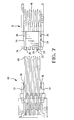
- Fig. 1 is a top front isometric view of upper and lower terminal inserts which comprise a terminal insert subassembly according to the invention;
- Fig. 2 is a top front isometric view of the terminal insert subassembly in assembled condition;
- Fig. 3 is a bottom rear isometric view of the upper and lower terminal inserts;
- Fig. 4 is a bottom rear isometric view of the terminal insert subassembly;
- Fig. 5 is a rear isometric view of the lower terminal insert;
- Fig. 6 is a front isometric view of the upper terminal insert;
- Fig. 7 is a top plan view of the upper and lower terminal inserts;
- Fig. 8 is a top plan view of the terminal insert subassembly;
- Fig. 9 is a side view of the terminal insert subassembly;
- Fig. 10 is a bottom view of the terminal insert subassembly;
- Fig. 11 is a cross-sectional view taken along line 11-11 in Fig. 10; and
- Fig. 12 is a cross-sectional view taken along line 12-12 in Fig. 10.
-
- There is shown in Figs. 2 and 4 a
terminal insert subassembly 4 which is adapted for use in an electrical connector of a type known as a stacked modular jack such as is disclosed in U.S. Patent No. 5,531,612 which is incorporated by reference as if set forth fully herein. As shown in the '612 patent, the stacked modular jack comprises a housing having a plurality of modular jack receptacles each of which can receive a mating modular plug. The receptacles are arranged in two rows which can be termed an upper row and a lower row. Extending into each of the receptacles is an array of terminals that are arranged in accordance with an industry standard configuration such as for an RJll or RJ45 style modular jack. Each terminal array is separately formed as a terminal insert which can be installed in the housing. Each terminal insert includes an insulative member which holds a plurality of terminals in the fixed array. The terminal inserts are either upper terminal inserts or lower terminal inserts which correspond to the upper and lower receptacles, respectively. Theterminal insert subassembly 4 comprises alower terminal insert 10 and anupper terminal insert 40, as shown in Figs. 1 and 3. - The
lower terminal insert 10 includes a lowerinsulative member 12 and a plurality ofterminals 14. Each of the terminals has a horizontally extending retention section 16 (shown in Figs. 11 and 12) which is secured in the lower insulative member, aforward mating section 18 which is engageable with a terminal of a mating modular plug, and adownward section 20 which terminates in acompliant pin lead 22 that is resiliently insertable in a through-hole in a circuit board (not shown) for electrical and mechanical engagement with the circuit board. Abend section 24 transitions between theretention section 16 and thedownward section 20. Exposed portions of the terminals at the rear of the lower insulative member include thedownward sections 20 and thebend sections 24. The exposed portions are defined by a lack of insulative material on at least one side of the terminals. The absence of material surrounding the terminals at the rear of the lower insulative member minimizes the size and cost of the lower insulative member. - As best seen in Fig. 5, the lower insulative member has a series of
support bars 26 andslots 28 between the support bars. Thedownward sections 20 of the terminals are arranged in twolateral terminal rows terminal row 29 are disposed in theslots 28, and the downward sections in theterminal row 30 are disposed innotches 32 in the ends of thesupport bars 26. Theslots 28 and thenotches 32 help to align, stabilize and support the downward sections of the terminals which are exposed at the rear of the lower insulative member. Further stabilization and support for the exposed portions of the terminals is provided by theupper terminal insert 40 as will be described. Referring back to Figs. 1 and 3, theupper terminal insert 40 includes an upperinsulative member 42 and a plurality ofterminals 44. Each of the terminals has a vertically extending retention section 46 (shown in Figs. 11 and 12) which is secured in the upper insulative member. Each of the terminals extends horizontally to aforward mating section 48 which is engageable with a terminal of a mating modular plug. An opposite end of each terminal includes acompliant pin lead 52 for electrical and mechanical engagement with a circuit board. - A forward portion of the upper insulative member provides support surfaces which are configured to confront the exposed portions of the terminals at the rear of the lower terminal insert. As best seen in Fig. 6, the upper insulative member has an array of forwardly extending
ribs 56 and inwardly extendinggrooves 58. Theribs 56 are configured to fit in theslots 28 between thesupport bars 26 of the lower insulative member. Extending from eachrib 56 is aprojection 60 having acurvilinear undersurface 62 which transitions to afront surface 64 of therib 56. Theundersurfaces 62 and thefront surfaces 64 are configured to closely confront the exposed portions of the terminals in theterminal row 29. In this way, theundersurfaces 62 and thefront surfaces 64 serve as support surfaces for the exposed portions of the terminals in theterminal row 29 when the compliant pin leads 22 of these terminals are installed in a circuit board. Further, the exposed portions of the terminals in theterminal row 30 are received in thegrooves 58. A downwardly facingsurface 66 and a forwardly facingsurface 68 within each of the grooves serve as support surfaces for the exposed portions of the terminals in theterminal row 30. - Referring now to Figs. 7 and 8, the
upper terminal insert 40 hasramps 70 and rearwardly facinglatches 72. Thelower terminal insert 10 hasramps 34 and forwardly facinglatches 36. Thelatches - As shown in Figs. 11 and 12, when the upper and lower terminal inserts are latched together, the
support surfaces bend sections 24 and thedownward sections 20 which are exposed at the rear of the lower terminal insert. Thesupport surfaces
Claims (6)
- An insert subassembly (4) for an electrical connector comprising a lower terminal insert (10) including a lower insulative member (12) which carries terminals (14) that have exposed portions (20, 24) at a rear of the lower insulative member, the exposed portions extending downwardly to define leads (22) for the connector, and an upper terminal insert (40) including an upper insulative member (42) which carries terminals (44), the upper insulative member (42) having support surfaces (62, 64, 66, 68) which confront the exposed portions (20, 24) of the terminals of the lower insulative member to provide support for the exposed portions when the leads (22) are engaged with a circuit board.
- The insert subassembly of claim 1 wherein the upper insulative member (12) includes forwardly extending ribs (56), and the support surfaces (64) are defined by front surfaces of the forwardly extending ribs.
- The insert subassembly of claims 1 or 2 wherein the upper insulative member (12) includes forwardly extending projections (60), and the support surfaces (62) are by undersurfaces of the forwardly extending projections.
- The insert subassembly of claims 1, 2 or 3 wherein the upper insulative member includes grooves (58) between forwardly extending ribs (56), and the support surfaces (66, 68) are defined by wall surfaces within each of the grooves.
- The insert subassembly of any preceding claim wherein the lower terminal insert and the upper terminal insert have mutually cooperable latches (36, 72).
- The insert subassembly of any preceding claim wherein one end of the terminals (44) of the upper insulative member include forward mating sections (48) for engagement with a terminal of a mating modular plug and the other end of the terminals (44) include leads for engagement with a circuit board.
Applications Claiming Priority (2)
| Application Number | Priority Date | Filing Date | Title |
|---|---|---|---|
| US86733 | 1998-05-29 | ||
| US09/086,733 US6042393A (en) | 1998-05-29 | 1998-05-29 | Support for compliant pin terminals |
Publications (3)
| Publication Number | Publication Date |
|---|---|
| EP0961366A2 true EP0961366A2 (en) | 1999-12-01 |
| EP0961366A3 EP0961366A3 (en) | 2001-09-12 |
| EP0961366B1 EP0961366B1 (en) | 2008-08-06 |
Family
ID=22200533
Family Applications (1)
| Application Number | Title | Priority Date | Filing Date |
|---|---|---|---|
| EP99303915A Expired - Lifetime EP0961366B1 (en) | 1998-05-29 | 1999-05-20 | Support for compliant pin terminals |
Country Status (3)
| Country | Link |
|---|---|
| US (1) | US6042393A (en) |
| EP (1) | EP0961366B1 (en) |
| CN (1) | CN1238578A (en) |
Cited By (2)
| Publication number | Priority date | Publication date | Assignee | Title |
|---|---|---|---|---|
| EP0961366A3 (en) * | 1998-05-29 | 2001-09-12 | The Whitaker Corporation | Support for compliant pin terminals |
| EP3382813A1 (en) * | 2017-03-29 | 2018-10-03 | Tyco Electronics France SAS | Support assembly for press-fit contact pins |
Families Citing this family (1)
| Publication number | Priority date | Publication date | Assignee | Title |
|---|---|---|---|---|
| US7458274B2 (en) * | 2007-02-20 | 2008-12-02 | Honeywell International Inc. | Pressure sensor incorporating a compliant pin |
Citations (4)
| Publication number | Priority date | Publication date | Assignee | Title |
|---|---|---|---|---|
| US4469387A (en) * | 1982-08-23 | 1984-09-04 | Amp Incorporated | Printed circuit board connector |
| US4857017A (en) * | 1987-04-24 | 1989-08-15 | Maxconn, Inc. | Support device for wires in multi-contact connectors |
| US5419720A (en) * | 1994-03-16 | 1995-05-30 | Chen; Michael | Structure of jack for modular plugs |
| US5639267A (en) * | 1996-01-26 | 1997-06-17 | Maxconn Incorporated | Modular jack assembly |
Family Cites Families (5)
| Publication number | Priority date | Publication date | Assignee | Title |
|---|---|---|---|---|
| GB2271678B (en) * | 1993-12-03 | 1994-10-12 | Itt Ind Ltd | Electrical connector |
| GB9325594D0 (en) * | 1993-12-14 | 1994-02-16 | Amp Great Britain | Multi-port modular jack assembly |
| US5562507A (en) * | 1994-11-25 | 1996-10-08 | Kan; Bright | Two-layer type multi-wire connection socket structure |
| US5599209A (en) * | 1994-11-30 | 1997-02-04 | Berg Technology, Inc. | Method of reducing electrical crosstalk and common mode electromagnetic interference and modular jack for use therein |
| US6042393A (en) * | 1998-05-29 | 2000-03-28 | The Whitaker Corporation | Support for compliant pin terminals |
-
1998
- 1998-05-29 US US09/086,733 patent/US6042393A/en not_active Expired - Lifetime
-
1999
- 1999-05-20 EP EP99303915A patent/EP0961366B1/en not_active Expired - Lifetime
- 1999-05-28 CN CN99106956A patent/CN1238578A/en active Pending
Patent Citations (4)
| Publication number | Priority date | Publication date | Assignee | Title |
|---|---|---|---|---|
| US4469387A (en) * | 1982-08-23 | 1984-09-04 | Amp Incorporated | Printed circuit board connector |
| US4857017A (en) * | 1987-04-24 | 1989-08-15 | Maxconn, Inc. | Support device for wires in multi-contact connectors |
| US5419720A (en) * | 1994-03-16 | 1995-05-30 | Chen; Michael | Structure of jack for modular plugs |
| US5639267A (en) * | 1996-01-26 | 1997-06-17 | Maxconn Incorporated | Modular jack assembly |
Cited By (4)
| Publication number | Priority date | Publication date | Assignee | Title |
|---|---|---|---|---|
| EP0961366A3 (en) * | 1998-05-29 | 2001-09-12 | The Whitaker Corporation | Support for compliant pin terminals |
| EP3382813A1 (en) * | 2017-03-29 | 2018-10-03 | Tyco Electronics France SAS | Support assembly for press-fit contact pins |
| FR3064826A1 (en) * | 2017-03-29 | 2018-10-05 | Tyco Electronics France Sas | SUPPORT ASSEMBLY FOR PRESSURE ADJUSTED CONTACT PINS |
| US10587063B2 (en) | 2017-03-29 | 2020-03-10 | Tyco Electronics France Sas | Support assembly for press-fit contact pins |
Also Published As
| Publication number | Publication date |
|---|---|
| EP0961366A3 (en) | 2001-09-12 |
| US6042393A (en) | 2000-03-28 |
| CN1238578A (en) | 1999-12-15 |
| EP0961366B1 (en) | 2008-08-06 |
Similar Documents
| Publication | Publication Date | Title |
|---|---|---|
| EP0880808B1 (en) | Shielded electrical connector | |
| US6379187B2 (en) | Electrical connector | |
| EP0795929B1 (en) | Electric connector assembly with improved retention characteristics | |
| EP0922318B1 (en) | Board-mountable electrical connector | |
| US4571017A (en) | Electrical connector assembly | |
| EP0347097B1 (en) | Electrical connector system | |
| EP0749182B1 (en) | Electrical connector with terminal tail aligning device | |
| US6457993B1 (en) | Modular jack with LED | |
| US5993263A (en) | Reduced mating force electrical connector | |
| JPH0797507B2 (en) | Jack for modular plug | |
| US5281165A (en) | Electrical connector shroud adapted for shorting bar removal | |
| US5674078A (en) | Multi-directional interface header assembly | |
| CN113451808A (en) | Electric connecting device and terminal | |
| US4474418A (en) | Electrical connector assembly | |
| EP0996993B1 (en) | Latched and shielded electrical connectors | |
| EP0488349B1 (en) | Connector with contact spacer plate having tapered channels | |
| US6322387B2 (en) | Latching connector assembly | |
| US5190483A (en) | Contact retention | |
| US6042393A (en) | Support for compliant pin terminals | |
| EP0374307A1 (en) | Connector assembly for printed circuit boards | |
| WO2022039053A1 (en) | Connector | |
| CN214505926U (en) | Socket connector, plug connector and combination thereof | |
| US6780063B2 (en) | Wire connected modular jack and assembling method | |
| US6210214B1 (en) | Stacked modular jack connector assembly | |
| EP1052733A1 (en) | Electrical connector with a contact locking element |
Legal Events
| Date | Code | Title | Description |
|---|---|---|---|
| PUAI | Public reference made under article 153(3) epc to a published international application that has entered the european phase |
Free format text: ORIGINAL CODE: 0009012 |
|
| AK | Designated contracting states |
Kind code of ref document: A2 Designated state(s): AT BE CH CY DE DK ES FI FR GB GR IE IT LI LU MC NL PT SE Kind code of ref document: A2 Designated state(s): DE FR GB IE IT NL SE |
|
| AX | Request for extension of the european patent |
Free format text: AL;LT;LV;MK;RO;SI |
|
| PUAL | Search report despatched |
Free format text: ORIGINAL CODE: 0009013 |
|
| AK | Designated contracting states |
Kind code of ref document: A3 Designated state(s): AT BE CH CY DE DK ES FI FR GB GR IE IT LI LU MC NL PT SE |
|
| AX | Request for extension of the european patent |
Free format text: AL;LT;LV;MK;RO;SI |
|
| 17P | Request for examination filed |
Effective date: 20020308 |
|
| AKX | Designation fees paid |
Free format text: DE FR GB IE IT NL SE |
|
| 17Q | First examination report despatched |
Effective date: 20070606 |
|
| GRAP | Despatch of communication of intention to grant a patent |
Free format text: ORIGINAL CODE: EPIDOSNIGR1 |
|
| GRAS | Grant fee paid |
Free format text: ORIGINAL CODE: EPIDOSNIGR3 |
|
| GRAA | (expected) grant |
Free format text: ORIGINAL CODE: 0009210 |
|
| RIC1 | Information provided on ipc code assigned before grant |
Ipc: H01R 24/06 20060101AFI20080624BHEP |
|
| AK | Designated contracting states |
Kind code of ref document: B1 Designated state(s): DE FR GB IE IT NL SE |
|
| REG | Reference to a national code |
Ref country code: GB Ref legal event code: FG4D |
|
| REG | Reference to a national code |
Ref country code: IE Ref legal event code: FG4D |
|
| REF | Corresponds to: |
Ref document number: 69939235 Country of ref document: DE Date of ref document: 20080918 Kind code of ref document: P |
|
| PG25 | Lapsed in a contracting state [announced via postgrant information from national office to epo] |
Ref country code: NL Free format text: LAPSE BECAUSE OF FAILURE TO SUBMIT A TRANSLATION OF THE DESCRIPTION OR TO PAY THE FEE WITHIN THE PRESCRIBED TIME-LIMIT Effective date: 20080806 |
|
| PLBE | No opposition filed within time limit |
Free format text: ORIGINAL CODE: 0009261 |
|
| STAA | Information on the status of an ep patent application or granted ep patent |
Free format text: STATUS: NO OPPOSITION FILED WITHIN TIME LIMIT |
|
| 26N | No opposition filed |
Effective date: 20090507 |
|
| PG25 | Lapsed in a contracting state [announced via postgrant information from national office to epo] |
Ref country code: IT Free format text: LAPSE BECAUSE OF FAILURE TO SUBMIT A TRANSLATION OF THE DESCRIPTION OR TO PAY THE FEE WITHIN THE PRESCRIBED TIME-LIMIT Effective date: 20080806 |
|
| PG25 | Lapsed in a contracting state [announced via postgrant information from national office to epo] |
Ref country code: SE Free format text: LAPSE BECAUSE OF FAILURE TO SUBMIT A TRANSLATION OF THE DESCRIPTION OR TO PAY THE FEE WITHIN THE PRESCRIBED TIME-LIMIT Effective date: 20081106 |
|
| REG | Reference to a national code |
Ref country code: IE Ref legal event code: MM4A |
|
| PG25 | Lapsed in a contracting state [announced via postgrant information from national office to epo] |
Ref country code: IE Free format text: LAPSE BECAUSE OF NON-PAYMENT OF DUE FEES Effective date: 20090520 |
|
| REG | Reference to a national code |
Ref country code: FR Ref legal event code: PLFP Year of fee payment: 18 |
|
| REG | Reference to a national code |
Ref country code: FR Ref legal event code: PLFP Year of fee payment: 19 |
|
| REG | Reference to a national code |
Ref country code: FR Ref legal event code: PLFP Year of fee payment: 20 |
|
| PGFP | Annual fee paid to national office [announced via postgrant information from national office to epo] |
Ref country code: DE Payment date: 20180508 Year of fee payment: 20 |
|
| PGFP | Annual fee paid to national office [announced via postgrant information from national office to epo] |
Ref country code: FR Payment date: 20180411 Year of fee payment: 20 |
|
| PGFP | Annual fee paid to national office [announced via postgrant information from national office to epo] |
Ref country code: GB Payment date: 20180516 Year of fee payment: 20 |
|
| REG | Reference to a national code |
Ref country code: DE Ref legal event code: R071 Ref document number: 69939235 Country of ref document: DE |
|
| REG | Reference to a national code |
Ref country code: GB Ref legal event code: PE20 Expiry date: 20190519 |
|
| PG25 | Lapsed in a contracting state [announced via postgrant information from national office to epo] |
Ref country code: GB Free format text: LAPSE BECAUSE OF EXPIRATION OF PROTECTION Effective date: 20190519 |