EP0961216B1 - IC card-based test apparatus and method - Google Patents
IC card-based test apparatus and method Download PDFInfo
- Publication number
- EP0961216B1 EP0961216B1 EP99200839A EP99200839A EP0961216B1 EP 0961216 B1 EP0961216 B1 EP 0961216B1 EP 99200839 A EP99200839 A EP 99200839A EP 99200839 A EP99200839 A EP 99200839A EP 0961216 B1 EP0961216 B1 EP 0961216B1
- Authority
- EP
- European Patent Office
- Prior art keywords
- smart card
- measurement
- interface
- card interface
- response
- Prior art date
- Legal status (The legal status is an assumption and is not a legal conclusion. Google has not performed a legal analysis and makes no representation as to the accuracy of the status listed.)
- Expired - Lifetime
Links
Images


Classifications
-
- G—PHYSICS
- G06—COMPUTING OR CALCULATING; COUNTING
- G06F—ELECTRIC DIGITAL DATA PROCESSING
- G06F11/00—Error detection; Error correction; Monitoring
- G06F11/22—Detection or location of defective computer hardware by testing during standby operation or during idle time, e.g. start-up testing
- G06F11/26—Functional testing
- G06F11/261—Functional testing by simulating additional hardware, e.g. fault simulation
-
- G—PHYSICS
- G06—COMPUTING OR CALCULATING; COUNTING
- G06K—GRAPHICAL DATA READING; PRESENTATION OF DATA; RECORD CARRIERS; HANDLING RECORD CARRIERS
- G06K7/00—Methods or arrangements for sensing record carriers, e.g. for reading patterns
- G06K7/0008—General problems related to the reading of electronic memory record carriers, independent of its reading method, e.g. power transfer
Definitions
- the present invention relates to an IC card-based test apparatus and method, and more particularly but not exclusively to the use of an IC card or the like for testing channel decoder apparatus.
- the interface requires the decoding apparatus to operate within certain limits as defined by a specification.
- There are numerous interface standards in use for example ISO, NDC (NDS), EMV and GSM.
- the decoding apparatus itself may be made by manufacturers not in any way associated with the makers of the smart cards.
- the decoding apparatus is usually made with interface parameters that lie within tolerances defined by the specification but sometimes some of the parameters are slightly out. Generally only a small number of features are marginally outside the specified tolerance with the result that the apparatus will work with most smart cards but not with all. This makes the apparatus very hard to test for all circumstances and very annoying for customers who find that their apparatus works well for several months and then fails following acquisition of a new smartcard.
- DE-A-19542262 discloses a test device for testing a smart card interface comprising a smart card front end configured for insertion into a smart card interface; a smart card input/output pad disposed on said smart card front end configured for interfacing with a smart card interface; a smart card chip electronically connected to said smart card input/output pad.
- the present invention is characterised in that said smart card chip is configured for performing a smart card interaction mimicking a smart card to be used with a particular smart card interface, said smart card interaction including receiving a response from a smart card interface; and a measurement and processing arrangement configured for determining a measurement of said response from a smart card interface; and comparing said measurement to specified design parameters of a smart card interface.
- the measurement and processing arrangement may be configured for terminating said smart card interaction between said smart card chip and the smart card interface when said measurement lies outside of the specified design parameters.
- the measurement may be a measurement of at least one of a high level and a low level of said response.
- the measurement may be a measurement of at least one of a rise time and a fall time of said response.
- the device may further comprise a display for displaying information indicative of the result of comparing said measurement to said specified design parameters.
- the display may be configured for indicating at least one of success and failure of the smart card interface to operate within the specified design parameters.
- the display includes at least one light emitting diode.
- the device may further comprise an output interface operationally connected to said measurement and processing arrangement, said output interface being configured for outputting the result of said comparing to a computer.
- the invention also provides a method for testing a smart card interface with a test device, the test device having a smart card chip, the method comprising the steps of, inserting the test device into the smart card interface; performing a smart card interaction with the smart card interface, said smart card interaction including receiving a response from the smart card interface; determining a measurement of said response; comparing said measurement to the specified design parameters of the smart card interface; and performing an action based on a result of said comparing.
- the general principle of the invention is that a zero tolerance, or worst case, smart card that has all of the functions of a standard smart card as handed out to customers, can be used to operate decoders in the normal manner. Because it is zero tolerance, any decoder that is even marginally out of spec in any vital parameter may fail the test and be discarded. Only those machines able to work with any smart card are thus likely be released onto the market.
- the smart card does not work like a standard test device.
- a standard test device connects to test pins on an IC and outputs signals that operate test circuits on the IC.
- the output signals generated are tested for their integrity and from this conclusions are drawn as to the circuit as a whole.
- the principle behind the present invention does not use test pins. Rather the circuit to be tested is operated in the normal way and monitoring is carried out of the standard in-use outputs.
- test time can be reduced to around ten minutes.
- test time is reduced to the normal interaction time of the smart card with the interface, that is to say around a few seconds. This is because, as explained, the present invention does not seek to test all of the functions and all of the inputs and outputs of the IRD. Rather it simply carries out the normal smart card interaction, receives the normal IRD responses and measures the responses against its prestored standards.
- the worst case smart card of the invention can be a standalone card or it can be built integrally with the electronics needed to test the successful operation of the decoder.
- Figure 1 is a block diagram of an embodiment operative in accordance with the present invention.
- Figure 1 shows an integrated receiver decoder (IRD) 10 to be tested for compliance with the relevant standards.
- a worst case smart card is incorporated into a test device 12.
- the test device 12 comprises a smart card chip 14 and standard I/O pad 16 which together provide a standard smart card interface for the IRD 10.
- a micro-processor 18 controls the smart card chip 14 and various other circuits in the test device 12.
- the various other circuits in the device include measurement electronics 20 operable to carry out measurements on output signals from the IRD 10.
- An LED (or similar) display 22 may optionally be provided to display device status information, error information or the like. Power is preferably made available from an external power supply but may be internal in some embodiments.
- An output 26 allows the device to be connected to a computer or the like. The output allows detailed diagnostic information that cannot be shown on the LED display 22, to be obtained.
- the front end 28 of the device 12 is shaped like a smart card so that it can be slotted directly into the smart card receiver slot (not shown) of the IRD 10.
- the device 12 is inserted, using its front end 28, into the IRD 10. It passes the information needed to enable the IRD 10 to start working and selectively measures outputs. That is to say it behaves to the IRD as a mimic of the real smartcard and measures outputs in the background to determine whether the outputs are within spec. If the outputs are outside the specification then the device 12 refuses to work.
- Examples of the features that can be measured include the duty cycle of the IRD.
- the duty cycle is specified in many of the interface specifications as having to be between 45% and 55%.
- the majority of smartcards will work with an IRD having a duty cycle that lies within the larger range of 40% to 60%, but a minority will not.
- Embodiments of the invention can be used to measure the duty cycle and exclude those machines that may cause a minority of smart cards to fail because of the excessive width of the duty cycle.
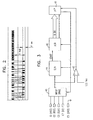
- Figure 2 is a schematic version of the output of an oscilloscope connected to the I/O line of the IRD 10.
- a typical specification may require the high level to be between 3.8V and Vcc.
- the low output may be specified as lying between 0V and 0.5V.
- Figure 3 is a block diagram showing circuitry that may typically be used to measure the high and low levels of the I/O line.
- An input stage 40 receives a series of signals C1, C2, C3, and C7.
- a comparator 42 decides whether the output of the input stage 40 is a high or a low signal by comparing the output with a reference signal set to 1/2 Vcc.
- S/H device 44 measures the amplitude of the signal and the output thereof is converted into a digital signal by A/D converter 46, which digital signal is passed to the microprocessor 18.
- a third example of a parameter that may be measured is the rise/fall time of the same signal.
- An oscillogram of this parameter is shown in figure 4. This is required by the various specifications to be typically below 0.1 ⁇ s.
- the feature may be measured by the circuitry shown in figure 5.
- a series of signals C1, C2, and C7 are received by an input stage 50.
- the microprocessor 18 chooses which of the input signals to measure.
- a comparator 52 watches for a high signal to fall 10%, (or for a low signal to rise by 10%) and then a counter 54 is started. The counter 54 continues to run until the comparator 52 notifies it that the signal has fallen (risen) to 90%. The final output of the counter is output to the microprocessor.
- An oscillator 56 provides a timing signal for the counter.
Landscapes
- Engineering & Computer Science (AREA)
- Theoretical Computer Science (AREA)
- Computer Hardware Design (AREA)
- General Engineering & Computer Science (AREA)
- Physics & Mathematics (AREA)
- General Physics & Mathematics (AREA)
- Quality & Reliability (AREA)
- Artificial Intelligence (AREA)
- Computer Vision & Pattern Recognition (AREA)
- Tests Of Electronic Circuits (AREA)
Description
- The present invention relates to an IC card-based test apparatus and method, and more particularly but not exclusively to the use of an IC card or the like for testing channel decoder apparatus.
- In the field of satellite and cable broadcasting it is well-known to provide pay channels that are only made available to viewers who have paid a subscription. The channel itself is transmitted in scrambled form. The viewer is provided with decoding equipment as part of the receiver apparatus that he is provided with upon signing up. Upon payment of the subscription the viewer is provided with a smart card that contains key information enabling the channel to be descrambled for the period of time covered by the subscription. Such an arrangement is known as a conditional access system.
- In order to implement such a conditional access system it is necessary to provide a defined interface between the smart card and the decoding equipment. The interface requires the decoding apparatus to operate within certain limits as defined by a specification. There are numerous interface standards in use, for example ISO, NDC (NDS), EMV and GSM. The decoding apparatus itself may be made by manufacturers not in any way associated with the makers of the smart cards. The decoding apparatus is usually made with interface parameters that lie within tolerances defined by the specification but sometimes some of the parameters are slightly out. Generally only a small number of features are marginally outside the specified tolerance with the result that the apparatus will work with most smart cards but not with all. This makes the apparatus very hard to test for all circumstances and very annoying for customers who find that their apparatus works well for several months and then fails following acquisition of a new smartcard.
- In general smartcards that are used in security applications are fast turnaround products due to the frequent need to replace some part of the security system, change a key or the like. The cards are thin and thus the chips inside are relatively hard to protect from damage. Therefore a great deal of research has gone in to smart card design. Smart card technology improves rapidly yet it is important that new, updated, smartcards remain compatible with old decoder boxes. In practice different generations of smartcard, as well as different batches of cards of the same generation, have different levels of tolerance to decoder box aberrations from specified ranges of signal parameters.
- DE-A-19542262 discloses a test device for testing a smart card interface comprising a smart card front end configured for insertion into a smart card interface; a smart card input/output pad disposed on said smart card front end configured for interfacing with a smart card interface; a smart card chip electronically connected to said smart card input/output pad.
- The present invention is characterised in that said smart card chip is configured for performing a smart card interaction mimicking a smart card to be used with a particular smart card interface, said smart card interaction including receiving a response from a smart card interface; and a measurement and processing arrangement configured for determining a measurement of said response from a smart card interface; and comparing said measurement to specified design parameters of a smart card interface.
- The measurement and processing arrangement may be configured for terminating said smart card interaction between said smart card chip and the smart card interface when said measurement lies outside of the specified design parameters.
- The measurement may be a measurement of at least one of a high level and a low level of said response.
- The measurement may be a measurement of at least one of a rise time and a fall time of said response.
- The device may further comprise a display for displaying information indicative of the result of comparing said measurement to said specified design parameters.
- The display may be configured for indicating at least one of success and failure of the smart card interface to operate within the specified design parameters.
- The display includes at least one light emitting diode.
- The device may further comprise an output interface operationally connected to said measurement and processing arrangement, said output interface being configured for outputting the result of said comparing to a computer.
- The invention also provides a method for testing a smart card interface with a test device, the test device having a smart card chip, the method comprising the steps of, inserting the test device into the smart card interface; performing a smart card interaction with the smart card interface, said smart card interaction including receiving a response from the smart card interface; determining a measurement of said response; comparing said measurement to the specified design parameters of the smart card interface; and performing an action based on a result of said comparing.
- For a better understanding of the invention and to show how the same may be carried into effect, reference will now be made, purely by way of example, to the accompanying drawings in which,
- Figure 1 shows a general block diagram of a device according to the invention and of a decoder to be measured by the device;
- Figure 2 shows an oscillogram of a signal output by a decoder device;
- Figure 3 is a block diagram of circuitry for measuring parameters of the signal of figure 2;
- Figure 4 shows a further oscillogram of the signal in figure 2; and
- Figure 5 is a block diagram of circuitry for measuring parameters of the signal shown in figure 4.
- The general principle of the invention is that a zero tolerance, or worst case, smart card that has all of the functions of a standard smart card as handed out to customers, can be used to operate decoders in the normal manner. Because it is zero tolerance, any decoder that is even marginally out of spec in any vital parameter may fail the test and be discarded. Only those machines able to work with any smart card are thus likely be released onto the market.
- In accordance with the present invention the smart card does not work like a standard test device. A standard test device connects to test pins on an IC and outputs signals that operate test circuits on the IC. The output signals generated are tested for their integrity and from this conclusions are drawn as to the circuit as a whole. The principle behind the present invention does not use test pins. Rather the circuit to be tested is operated in the normal way and monitoring is carried out of the standard in-use outputs.
- Indeed the current practice in the field of conditional access devices is to test every pin on the IRD. This is expensive and time-consuming but is currently seen as unavoidable if satisfactory operation of the system is to be guaranteed. Furthermore it does not predict the interaction of the decoder device and the chip.
- It is pointed out that at present it takes around six hours for a qualified technician to test an IRD by hand. With the very latest automated equipment the test time can be reduced to around ten minutes. With embodiments of the present invention the test time is reduced to the normal interaction time of the smart card with the interface, that is to say around a few seconds. This is because, as explained, the present invention does not seek to test all of the functions and all of the inputs and outputs of the IRD. Rather it simply carries out the normal smart card interaction, receives the normal IRD responses and measures the responses against its prestored standards.
- However, as the present invention demonstrates, if a worst-case smart card can successfully operate the device then it ceases to be necessary to check every single pin. Every other smart card that operates properly within the parameters set for the smart card should be able to operate the device.
- As will be discussed below, the worst case smart card of the invention can be a standalone card or it can be built integrally with the electronics needed to test the successful operation of the decoder.
- Figure 1 is a block diagram of an embodiment operative in accordance with the present invention. Figure 1 shows an integrated receiver decoder (IRD) 10 to be tested for compliance with the relevant standards. A worst case smart card is incorporated into a
test device 12. Thetest device 12 comprises asmart card chip 14 and standard I/O pad 16 which together provide a standard smart card interface for the IRD 10. A micro-processor 18 controls thesmart card chip 14 and various other circuits in thetest device 12. The various other circuits in the device includemeasurement electronics 20 operable to carry out measurements on output signals from theIRD 10. - An LED (or similar)
display 22 may optionally be provided to display device status information, error information or the like. Power is preferably made available from an external power supply but may be internal in some embodiments. Anoutput 26 allows the device to be connected to a computer or the like. The output allows detailed diagnostic information that cannot be shown on theLED display 22, to be obtained. - The
front end 28 of thedevice 12 is shaped like a smart card so that it can be slotted directly into the smart card receiver slot (not shown) of theIRD 10. - The
device 12 is inserted, using itsfront end 28, into theIRD 10. It passes the information needed to enable theIRD 10 to start working and selectively measures outputs. That is to say it behaves to the IRD as a mimic of the real smartcard and measures outputs in the background to determine whether the outputs are within spec. If the outputs are outside the specification then thedevice 12 refuses to work. - Examples of the features that can be measured include the duty cycle of the IRD. The duty cycle is specified in many of the interface specifications as having to be between 45% and 55%. The majority of smartcards will work with an IRD having a duty cycle that lies within the larger range of 40% to 60%, but a minority will not. Embodiments of the invention can be used to measure the duty cycle and exclude those machines that may cause a minority of smart cards to fail because of the excessive width of the duty cycle.
- A further example of a feature that can be measured is shown in figure 2. Figure 2 is a schematic version of the output of an oscilloscope connected to the I/O line of the
IRD 10. A typical specification may require the high level to be between 3.8V and Vcc. The low output may be specified as lying between 0V and 0.5V. - Figure 3 is a block diagram showing circuitry that may typically be used to measure the high and low levels of the I/O line. An
input stage 40 receives a series of signals C1, C2, C3, and C7. Acomparator 42 decides whether the output of theinput stage 40 is a high or a low signal by comparing the output with a reference signal set to 1/2 Vcc. S/H device 44 then measures the amplitude of the signal and the output thereof is converted into a digital signal by A/D converter 46, which digital signal is passed to themicroprocessor 18. - A third example of a parameter that may be measured is the rise/fall time of the same signal. An oscillogram of this parameter is shown in figure 4. This is required by the various specifications to be typically below 0.1 µs. The feature may be measured by the circuitry shown in figure 5. A series of signals C1, C2, and C7 are received by an
input stage 50. Themicroprocessor 18 chooses which of the input signals to measure. Acomparator 52 watches for a high signal to fall 10%, (or for a low signal to rise by 10%) and then acounter 54 is started. Thecounter 54 continues to run until thecomparator 52 notifies it that the signal has fallen (risen) to 90%. The final output of the counter is output to the microprocessor. Anoscillator 56 provides a timing signal for the counter. - In accordance with embodiments of the present invention it is thus possible to provide a worst case smartcard and to test for general compatibility of the device with the card simply by slotting the card into the device and operating the device in the normal way. No expensive laboratory equipment is needed and the time taken for each measurement is not excessive.
- The foregoing description is given by way of example only. The scope of protection is defined by the appended claims.
- It is appreciated that the various features of the invention which are, for clarity, described in the contexts of separate embodiments may also be provided in combination in a single embodiment. Conversely, various features of the invention which are, for brevity, described in the context of a single embodiment may also be provided separately or in any suitable subcombination.
Claims (9)
- A test device for testing a smart card interface comprising:a smart card front end (28) configured for insertion into a smart card interface;a smart card input/output pad (16) disposed on said smart card front end (28) configured for interfacing with a smart card interface;a smart card chip (14) electronically connected to said smart card input/output pad (16),characterised in that said smart card chip (14) is configured for performing a smart card interaction mimicking a smart card to be used with a particular smart card interface, said smart card interaction including receiving a response from a smart card interface; and
a measurement and processing arrangement (18, 20) configured for:determining a measurement of said response from a smart card interface; andcomparing said measurement to specified design parameters of a smart card interface. - The device according to claim 1, wherein said measurement and processing arrangement is configured for terminating said smart card interaction between said smart card chip (14) and the smart card interface when said measurement lies outside of the specified design parameters.
- The device according to claim 1 or 2, wherein said measurement is a measurement of at least one of a high level and a low level of said response.
- The device according to any of claims 1 to 3, wherein said measurement is a measurement of at least one of a rise time and a fall time of said response.
- The device according to any of claims 1 to 4, further comprising a display (22) for displaying information indicative of the result of comparing said measurement to said specified design parameters.
- The device according to claim 5, wherein said display (22) is configured for indicating at least one of success and failure of the smart card interface to operate within the specified design parameters.
- The device according to claim 5 or claim 6, wherein said display (22) includes at least one light emitting diode.
- The device according to any one preceding claim, further comprising an output interface (26) operationally connected to said measurement and processing arrangement (18, 20), said output interface (26) being configured for outputting the result of said comparing to a computer.
- A method for testing a smart card interface with a test device, the test device having a smart card chip, the method comprising the steps of:inserting the test device into the smart card interface;characterised by performing a smart card interaction with the smart card interface, said smart card interaction including receiving a response from the smart card interface;
determining a measurement of said response;
comparing said measurement to the specified design parameters of the smart card interface; and
performing an action based on a result of said comparing.
Applications Claiming Priority (2)
| Application Number | Priority Date | Filing Date | Title |
|---|---|---|---|
| IL12465598A IL124655A (en) | 1998-05-26 | 1998-05-26 | Ic card-based test apparatus and method |
| IL12465598 | 1998-05-26 |
Publications (3)
| Publication Number | Publication Date |
|---|---|
| EP0961216A2 EP0961216A2 (en) | 1999-12-01 |
| EP0961216A3 EP0961216A3 (en) | 2001-10-24 |
| EP0961216B1 true EP0961216B1 (en) | 2006-06-14 |
Family
ID=11071556
Family Applications (1)
| Application Number | Title | Priority Date | Filing Date |
|---|---|---|---|
| EP99200839A Expired - Lifetime EP0961216B1 (en) | 1998-05-26 | 1999-03-17 | IC card-based test apparatus and method |
Country Status (3)
| Country | Link |
|---|---|
| EP (1) | EP0961216B1 (en) |
| DE (1) | DE69931845T2 (en) |
| IL (1) | IL124655A (en) |
Families Citing this family (4)
| Publication number | Priority date | Publication date | Assignee | Title |
|---|---|---|---|---|
| KR20030091040A (en) * | 2002-05-22 | 2003-12-01 | 톰슨 라이센싱 소시에떼 아노님 | Device for receiving and/or for processing video signals, memory card, assembly composed of such a device and of such a card and process for controlling such a device |
| GB0306170D0 (en) * | 2003-03-18 | 2003-04-23 | Univ Staffordshire | Electronic test & diagnostic apparatus |
| EP1708517A1 (en) * | 2005-04-01 | 2006-10-04 | Advanced Digital Broadcast S.A. | Method for transmitting test data in an electronic device equipped with an electronic card reader, electronic device comprising an electronic card reader and an adapter for testing electronic devices equipped with an electronic card reader |
| CN106680625A (en) * | 2016-12-14 | 2017-05-17 | 新智数字科技有限公司 | Electronic card test method and test mainboard |
Family Cites Families (2)
| Publication number | Priority date | Publication date | Assignee | Title |
|---|---|---|---|---|
| DE19542262C2 (en) * | 1994-11-12 | 2001-12-13 | Fischer Computersysteme Gmbh & | Transportable interface |
| FR2737794B1 (en) * | 1995-08-10 | 1997-10-24 | Cantu Augusto Giuseppe Lucio | COMMUNICATION ADAPTER FOR ELECTRONIC CARD READERS |
-
1998
- 1998-05-26 IL IL12465598A patent/IL124655A/en not_active IP Right Cessation
-
1999
- 1999-03-17 EP EP99200839A patent/EP0961216B1/en not_active Expired - Lifetime
- 1999-03-17 DE DE69931845T patent/DE69931845T2/en not_active Expired - Fee Related
Also Published As
| Publication number | Publication date |
|---|---|
| DE69931845T2 (en) | 2007-01-11 |
| IL124655A0 (en) | 1998-12-06 |
| EP0961216A2 (en) | 1999-12-01 |
| DE69931845D1 (en) | 2006-07-27 |
| IL124655A (en) | 2001-03-19 |
| EP0961216A3 (en) | 2001-10-24 |
Similar Documents
| Publication | Publication Date | Title |
|---|---|---|
| US7185295B2 (en) | Chip design verifying and chip testing apparatus and method | |
| US6263170B1 (en) | Consumable component identification and detection | |
| US6479983B1 (en) | Semiconductor device testing apparatus having timing hold function | |
| US6766486B2 (en) | Joint test action group (JTAG) tester, such as to test integrated circuits in parallel | |
| US7554352B2 (en) | Method for determining information about the internal workings of a chip based on electro-magnetic emissions therefrom | |
| US20170242419A1 (en) | Dut continuity test with only digital io structures apparatus and methods associated thereof | |
| TWI424180B (en) | Adapter frame | |
| EP0239922A2 (en) | Input voltage signal check circuit for a semiconductor integrated circuit | |
| US20040059971A1 (en) | Device under test interface card with on-board testing | |
| KR101009375B1 (en) | Semiconductor integrated circuits and control methods thereof, and information processing apparatus | |
| GB2404265A (en) | Method and apparatus for testing an electronic device | |
| EP0961216A2 (en) | IC card-based test apparatus and method | |
| KR101906702B1 (en) | Integrated performance diagnosis system and method for integrated circuit board of reactor protection system | |
| CN110504000B (en) | Method for identifying probe card information of wafer-level test tester | |
| EP2093580A1 (en) | Supply current based testing of CMOS output stages | |
| US6986087B2 (en) | Method and apparatus for improving testability of I/O driver/receivers | |
| US20190056445A1 (en) | Dut continuity test with only digital io structures apparatus and methods associated thereof | |
| US20050251714A1 (en) | Test apparatus for semiconductor devices built-in self-test function | |
| US20050073788A1 (en) | Integrated circuit outputs protection during JTAG board tests | |
| CN102778629A (en) | Method and arrangement for automatically measuring electric connections of electronic circuit arrangements mounted on pcb | |
| US7282938B2 (en) | Testing apparatus and method for providing temperature stress to electronic component | |
| KR19990035741U (en) | Device to be tested using internal memory | |
| CN116258119B (en) | A System and Method for Verifying GPIO Pins of a SoC Chip | |
| US6791348B2 (en) | Digital overcurrent test | |
| US6898543B2 (en) | In-system testing of an oscillator |
Legal Events
| Date | Code | Title | Description |
|---|---|---|---|
| PUAI | Public reference made under article 153(3) epc to a published international application that has entered the european phase |
Free format text: ORIGINAL CODE: 0009012 |
|
| AK | Designated contracting states |
Kind code of ref document: A2 Designated state(s): AT BE CH CY DE DK ES FI FR GB GR IE IT LI LU MC NL PT SE Kind code of ref document: A2 Designated state(s): CH DE ES FR GB GR IT LI NL |
|
| AX | Request for extension of the european patent |
Free format text: AL;LT;LV;MK;RO;SI |
|
| PUAL | Search report despatched |
Free format text: ORIGINAL CODE: 0009013 |
|
| AK | Designated contracting states |
Kind code of ref document: A3 Designated state(s): AT BE CH CY DE DK ES FI FR GB GR IE IT LI LU MC NL PT SE |
|
| AX | Request for extension of the european patent |
Free format text: AL;LT;LV;MK;RO;SI |
|
| RIC1 | Information provided on ipc code assigned before grant |
Free format text: 7G 06K 7/00 A, 7G 06K 19/07 B, 7G 06F 11/273 B, 7G 01R 31/00 B, 7G 06K 19/077 B |
|
| 17P | Request for examination filed |
Effective date: 20011211 |
|
| AKX | Designation fees paid |
Free format text: CH DE ES FR GB GR IT LI NL |
|
| 17Q | First examination report despatched |
Effective date: 20050119 |
|
| GRAP | Despatch of communication of intention to grant a patent |
Free format text: ORIGINAL CODE: EPIDOSNIGR1 |
|
| GRAS | Grant fee paid |
Free format text: ORIGINAL CODE: EPIDOSNIGR3 |
|
| GRAA | (expected) grant |
Free format text: ORIGINAL CODE: 0009210 |
|
| AK | Designated contracting states |
Kind code of ref document: B1 Designated state(s): CH DE ES FR GB GR IT LI NL |
|
| PG25 | Lapsed in a contracting state [announced via postgrant information from national office to epo] |
Ref country code: IT Free format text: LAPSE BECAUSE OF FAILURE TO SUBMIT A TRANSLATION OF THE DESCRIPTION OR TO PAY THE FEE WITHIN THE PRESCRIBED TIME-LIMIT;WARNING: LAPSES OF ITALIAN PATENTS WITH EFFECTIVE DATE BEFORE 2007 MAY HAVE OCCURRED AT ANY TIME BEFORE 2007. THE CORRECT EFFECTIVE DATE MAY BE DIFFERENT FROM THE ONE RECORDED. Effective date: 20060614 |
|
| REG | Reference to a national code |
Ref country code: GB Ref legal event code: FG4D |
|
| RIN1 | Information on inventor provided before grant (corrected) |
Inventor name: ADLER, MICHAEL |
|
| REG | Reference to a national code |
Ref country code: CH Ref legal event code: EP |
|
| REF | Corresponds to: |
Ref document number: 69931845 Country of ref document: DE Date of ref document: 20060727 Kind code of ref document: P |
|
| PG25 | Lapsed in a contracting state [announced via postgrant information from national office to epo] |
Ref country code: ES Free format text: LAPSE BECAUSE OF FAILURE TO SUBMIT A TRANSLATION OF THE DESCRIPTION OR TO PAY THE FEE WITHIN THE PRESCRIBED TIME-LIMIT Effective date: 20060925 |
|
| REG | Reference to a national code |
Ref country code: CH Ref legal event code: NV Representative=s name: RITSCHER & PARTNER AG |
|
| ET | Fr: translation filed | ||
| PLBE | No opposition filed within time limit |
Free format text: ORIGINAL CODE: 0009261 |
|
| STAA | Information on the status of an ep patent application or granted ep patent |
Free format text: STATUS: NO OPPOSITION FILED WITHIN TIME LIMIT |
|
| PGFP | Annual fee paid to national office [announced via postgrant information from national office to epo] |
Ref country code: DE Payment date: 20070430 Year of fee payment: 9 |
|
| 26N | No opposition filed |
Effective date: 20070315 |
|
| REG | Reference to a national code |
Ref country code: CH Ref legal event code: PCAR Free format text: RITSCHER & PARTNER AG;RESIRAIN 1;8125 ZOLLIKERBERG (CH) |
|
| PG25 | Lapsed in a contracting state [announced via postgrant information from national office to epo] |
Ref country code: GR Free format text: LAPSE BECAUSE OF FAILURE TO SUBMIT A TRANSLATION OF THE DESCRIPTION OR TO PAY THE FEE WITHIN THE PRESCRIBED TIME-LIMIT Effective date: 20060915 |
|
| PG25 | Lapsed in a contracting state [announced via postgrant information from national office to epo] |
Ref country code: DE Free format text: LAPSE BECAUSE OF NON-PAYMENT OF DUE FEES Effective date: 20081001 |
|
| PGFP | Annual fee paid to national office [announced via postgrant information from national office to epo] |
Ref country code: NL Payment date: 20090324 Year of fee payment: 11 |
|
| REG | Reference to a national code |
Ref country code: GB Ref legal event code: 732E Free format text: REGISTERED BETWEEN 20090528 AND 20090603 |
|
| PGFP | Annual fee paid to national office [announced via postgrant information from national office to epo] |
Ref country code: CH Payment date: 20090325 Year of fee payment: 11 |
|
| PGFP | Annual fee paid to national office [announced via postgrant information from national office to epo] |
Ref country code: IT Payment date: 20090330 Year of fee payment: 11 |
|
| PGFP | Annual fee paid to national office [announced via postgrant information from national office to epo] |
Ref country code: FR Payment date: 20090317 Year of fee payment: 11 |
|
| PGFP | Annual fee paid to national office [announced via postgrant information from national office to epo] |
Ref country code: GB Payment date: 20090403 Year of fee payment: 11 |
|
| REG | Reference to a national code |
Ref country code: NL Ref legal event code: V1 Effective date: 20101001 |
|
| REG | Reference to a national code |
Ref country code: CH Ref legal event code: PL |
|
| GBPC | Gb: european patent ceased through non-payment of renewal fee |
Effective date: 20100317 |
|
| REG | Reference to a national code |
Ref country code: FR Ref legal event code: ST Effective date: 20101130 |
|
| PG25 | Lapsed in a contracting state [announced via postgrant information from national office to epo] |
Ref country code: NL Free format text: LAPSE BECAUSE OF NON-PAYMENT OF DUE FEES Effective date: 20101001 Ref country code: FR Free format text: LAPSE BECAUSE OF NON-PAYMENT OF DUE FEES Effective date: 20100331 |
|
| PG25 | Lapsed in a contracting state [announced via postgrant information from national office to epo] |
Ref country code: LI Free format text: LAPSE BECAUSE OF NON-PAYMENT OF DUE FEES Effective date: 20100331 Ref country code: CH Free format text: LAPSE BECAUSE OF NON-PAYMENT OF DUE FEES Effective date: 20100331 |
|
| PG25 | Lapsed in a contracting state [announced via postgrant information from national office to epo] |
Ref country code: IT Free format text: LAPSE BECAUSE OF NON-PAYMENT OF DUE FEES Effective date: 20100317 Ref country code: GB Free format text: LAPSE BECAUSE OF NON-PAYMENT OF DUE FEES Effective date: 20100317 |