EP0954100A1 - Cmos high voltage drive output buffer - Google Patents
Cmos high voltage drive output buffer Download PDFInfo
- Publication number
- EP0954100A1 EP0954100A1 EP99303031A EP99303031A EP0954100A1 EP 0954100 A1 EP0954100 A1 EP 0954100A1 EP 99303031 A EP99303031 A EP 99303031A EP 99303031 A EP99303031 A EP 99303031A EP 0954100 A1 EP0954100 A1 EP 0954100A1
- Authority
- EP
- European Patent Office
- Prior art keywords
- channel device
- voltage
- gate
- coupled
- vdd5
- Prior art date
- Legal status (The legal status is an assumption and is not a legal conclusion. Google has not performed a legal analysis and makes no representation as to the accuracy of the status listed.)
- Withdrawn
Links
- 230000005540 biological transmission Effects 0.000 claims abstract description 10
- 101150114468 TUB1 gene Proteins 0.000 claims description 21
- 101100098873 Chondrus crispus TUBB gene Proteins 0.000 claims description 18
- 101150025182 TUBB1 gene Proteins 0.000 claims description 18
- 238000005516 engineering process Methods 0.000 description 9
- 230000003071 parasitic effect Effects 0.000 description 4
- 238000010586 diagram Methods 0.000 description 3
- 238000000034 method Methods 0.000 description 2
- 239000000969 carrier Substances 0.000 description 1
- 230000001902 propagating effect Effects 0.000 description 1
- 230000000630 rising effect Effects 0.000 description 1
Images

Classifications
-
- H—ELECTRICITY
- H03—ELECTRONIC CIRCUITRY
- H03K—PULSE TECHNIQUE
- H03K19/00—Logic circuits, i.e. having at least two inputs acting on one output; Inverting circuits
- H03K19/003—Modifications for increasing the reliability for protection
- H03K19/00315—Modifications for increasing the reliability for protection in field-effect transistor circuits
-
- H—ELECTRICITY
- H03—ELECTRONIC CIRCUITRY
- H03K—PULSE TECHNIQUE
- H03K17/00—Electronic switching or gating, i.e. not by contact-making and –breaking
- H03K17/51—Electronic switching or gating, i.e. not by contact-making and –breaking characterised by the components used
- H03K17/56—Electronic switching or gating, i.e. not by contact-making and –breaking characterised by the components used by the use, as active elements, of semiconductor devices
- H03K17/567—Circuits characterised by the use of more than one type of semiconductor device, e.g. BIMOS, composite devices such as IGBT
-
- H—ELECTRICITY
- H03—ELECTRONIC CIRCUITRY
- H03K—PULSE TECHNIQUE
- H03K2217/00—Indexing scheme related to electronic switching or gating, i.e. not by contact-making or -breaking covered by H03K17/00
- H03K2217/0018—Special modifications or use of the back gate voltage of a FET
Definitions
- the present invention relates to a CMOS high voltage drive output buffer protection circuit and, more particularly, to a CMOS high voltage drive output buffer protection circuit formed in low voltage CMOS technology (e.g., 3.3V) that is tolerant of high input voltages (e.g., 5V).
- low voltage CMOS technology e.g., 3.3V
- high input voltages e.g., 5V
- CMOS circuit design In many areas of CMOS circuit design there are arrangements that include sections that run between 0-5V and other sections that use a voltage supply range of only 0-3.3V. There is often a need to provide a "buffer” circuit between these sections. Thus, there is a need to supply a circuit in standard low voltage CMOS technology (e.g., 3.3V) that can drive a relative high voltage (e.g., 5V) on its output. Additionally, many system configurations require a circuit that is "hot pluggable", meaning that the circuit will not draw any current from a bus that is at a high voltage, even when the circuit is not powered (i.e., when VDD is not present). Further, the circuit should be designed so that it is not “harmed” when exposed to relatively high voltages.
- CMOS technology e.g., 3.3V
- 5V relative high voltage
- CMOS buffer interfacing with a relatively high voltage is that the source of a P-channel output transistor is usually connected to the low voltage power supply VDD. If a voltage greater than VDD is applied to the drain of this device (where the drain is usually connected to the PAD of the buffer), it will forward bias the parasitic diode inherent in the P-channel device, since the N-tub backgate of the P-channel transistors is usually connected to VDD.
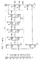
- buffer 10 capable of driving a relatively high voltage (5V) in a low voltage technology (e.g., 3V) is illustrated in FIG. 1.
- buffer circuit 10 is capable of driving 5V without the voltage across any transistor rising above the "low voltage" level.
- buffer 10 comprises a resistor divider tree 12 formed of a plurality ofN-tub resistors 14 1 - 14 7 disposed between VSS (ground) and VDD5 (the 5V power supply rail). Resistor divider tree 12 thus generates a plurality of different reference voltages, labeled VL1, VL2, VL3, VH1, VH2 and VH3 in FIG. 1.
- Resistors 14 1 - 14 7 are sized such that VL3 is one-third of VDD5 and VH1 is two-thirds of VDD5.
- the voltages VL1 and VL2 are evenly divided between VSS and VL3, and the voltages VH2 and VH3 are evenly divided between VDD5 and VH1.
- Transistors 16-34 form a tapered inverter chain 36 whose output voltages are slowly shifted from the 0-VDD (i.e., 0-3V) range to the VL3-VDD5 (i.e., 3.3-5V) range.
- a first inverter formed by transistors 16 and 18 is biased between VDD and VSS
- a second inverter formed by transistors 20 and 22
- the last inverter formed by transistors 32 and 34 biased between VL3 and VDD5.
- the output from inverter chain 36 is applied as the gate voltage to a P-channel transistor 38.
- Transistor 40 acts as a source-follower clamp to keep node B from ever going above VDD-Vtn (where Vtn is defined as the N-channel transistor threshold voltage) - even when a full 5V is applied to the PAD terminal.
- transistor 42 clamps node C from ever going below VL3 + Vtp (Vtp being a P-channel transistor threshold voltage) - even when the PAD terminal is held at zero.
- One known solution to the above "hot pluggable" problem is to utilize a relatively thick gate oxide for any devices that may be exposed to the relatively high voltages at their gate terminals and utilize a standard gate oxide for all remaining devices.
- transistors 38, 40 and 42 would require a thick oxide in order to be protected from PAD high voltages in the absence of VDD5.
- the use of two different gate oxide thicknesses is a very expensive technique that adds appreciable extra cost and process time to conventional CMOS processing technology.
- the present invention relates to a CMOS high voltage drive output buffer protection circuit and, more particularly, to a CMOS high voltage drive output buffer protection circuit formed in low voltage CMOS technology (i.e. 3.3V) that is tolerant of high voltage CMOS input voltages (i.e. 5V) and will not draw any current in the "no power" state (i.e., when VDD5 is not present).
- low voltage CMOS technology i.e. 3.3V
- high voltage CMOS input voltages i.e. 5V
- the drive stage portion of the circuit of FIG. 1 is replaced with a circuit capable of protecting the output transistors from being "stressed" during hot pluggable conditions.
- Biasing for the circuit of the present invention is provided, in part, by a reference voltage generator for generating a voltage VDD2 that will be equal to VDD as long as VDD is present, and when VDD is not present, VDD2 will track the PAD voltage (remaining a predetermined voltage less than PAD).
- An inverter biased between VL3 and VDD2, is used to generate a gate bias voltage to control the operation of the drive stage. Clamping transistors are included to insure that a full 5V does not appear across any device.
- An additional aspect of the present invention is to provide a backgate bias generator circuit that is hot pluggable and is capable of generating a 5V protection voltage for all P-channel devices within the inventive drive stage.
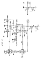
- FIG. 2 An exemplary drive stage 50 for use with the buffer circuit of FIG. 1 is shown in FIG. 2.
- Drive stage 50 is used to replace transistors 38, 40, 42 and 43 of the prior art buffer circuit of FIG. 1 and results in forming a "hot pluggable" 5V drive output buffer.
- Nodes P and N of FIG. 1 are illustrated as the same nodes P and N in FIG. 2 and are used to drive the circuit of the present invention.
- a reference voltage VDD2 is also applied as an input to drive stage 50.
- Reference voltage VDD2 is generated to be equal to VDD as along as VDD is present, and when VDD is not present (hot pluggable conditions), VDD2 will be maintained at a predetermined voltage less than the PAD voltage (usually, approximately two diode drops less than PAD).
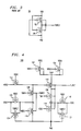
- FIG. 5 An exemplary circuit for generating reference voltage VDD2 is illustrated in FIG. 5.
- a CMOS reference voltage generator 130 is configured such that a generated reference voltage VDD2 is essentially equal to the power supply VDD as long as VDD is "present” (typically 3.0 - 3.6 volts, but in general any voltage above approximately 1V), regardless of the voltage on the signal bus (“PAD”), which may rise to, for example, 5V if a mix of CMOS technology is present in the circuit.
- PAD voltage on the signal bus
- VDD2 VDD.
- transistors 52, 54, 56 and 58 function is a manner similar to transistors 38, 42, 40 and 43 (respectively) of the prior art circuit.
- the similar functionality is provided by using an inverter 60, consisting of a P-channel device 62 and N-channel device 64, coupled between VDD2 and VL3, as shown in FIG. 2.
- the input to the inverter is the power supply voltage VDD and the output is defined as PGATE.
- PGATE will be equal to VL3.
- PGATE is applied as an input to a transmission gate formed by a P-channel device 66 and an N-channel device 67.
- PGATE is applied as the gate control voltage to P-channel device 66, keeping device 66 "on” such that the signal appearing at input node P can be transferred to output node P0, allowing node P0 to follow input P all the way from VDD5 to VL3.
- Node P0 is coupled to the gate of P-channel device 52, where device 52 functions in a manner similar to device 38 ofthe prior art circuit of FIG. 1. Since transistors 68 and 70 will be "off” (as long as VDD5 is present, the gates of transistors 68 and 70 will be held at VDD5 and the transistors will not conduct), the full P voltage will appear at the gate of device 52.
- the gate of N-channel device 72 is held at VDD and the gate of N-channel device 74 is held at VDD2.
- VDD2 VDD and both devices will be "on”. Therefore, the full voltage level VL3 will appear at the gate of P-channel device 54, defined as node P1 in FIG. 2.
- Reference voltage TUB 1 discussed below in association with the backgate bias generator circuit of FIG.
- VDD5 is defined as equal to VDD5 and is applied as the gate voltage to a P-channel device 76 where the source of device 76 is coupled to node P1. Since device 76 will be "off' as long as VDD5 is present, the voltage appearing at node P1 will be the full VL3 voltage level. Device 54 will thus function to prevent the voltage appearing at node C from dropping below VL3+Vtp (in a manner similar to device 42 of FIG. 1) during "normal” conditions (that is, as long as VDD and VDD5 are present).
- N-channel device 72 With the absence of VDD, N-channel device 72 will turn “off” .
- the lower voltage VDD2 appearing at the gate of N-channel device 74 will allow device 74 to act as a clamp, protecting the gate oxide of device 72.
- output voltage PGATE will rise to VDD2, resulting in turning "off' P-channel device 66.
- N-channel device 67 Since VDD5 is not present, N-channel device 67 will also be “off”, thereby preventing the voltage at P0 from propagating through the transmission gate to node P.
- the absence of VDD5 will also turn “on” P-channel devices 68 and 70.
- P-channel devices 68 and 70 function to clamp nodes P0 and C at the VDD2 voltage level.
- the P-channel devices may utilize a voltage, defined as TUBFLT, that is applied to the N-tub of each device. It is well-known that by biasing the tub region of these devices, a P-channel device can be used at a voltage above the power supply without turning on its inherent parasitic diode.
- FIG. 3 illustrates a conventional prior art arrangement used to generate the TUBFLT voltage.
- Generator circuit 90 includes a pair of P-channel devices 92 and 94 that are disposed between VDD and PAD voltage potentials. The gate of transistor 92 is coupled to the PAD voltage and the gate of transistor 94 is coupled to VDD. In normal operation, the PAD voltage is between 0 and VDD. In this case, transistor 92 is turned “on” and transistors 94 is “off'. Therefore, output voltage TUBFLT will be equal to VDD. When the PAD voltage rises above VDD by one P-channel threshold voltage, transistor 94 will turn “on” and transistor 92 will turn “off”. TUBFLT will now be equal to the PAD voltage.
- circuit 90 cannot be used in a low voltage CMOS technology to generate a backgate voltage large enough to bias the N-tubs of transistors that may have a 5V potential applied to their source or drain, since if the VDD voltage as shown in FIG. 3 were allowed to rise to the 5V level, then the entire 5V would be placed on the gate oxide of device 92 whenever PAD was at 0V.
- FIG. 4 illustrates an exemplary N-tub backgate bias generator 100 of the present invention that is capable of generating an output voltage TUBFLT equal to VDD5 when the PAD voltage is less than VDD5, and an output voltage TUBFLT equal to the PAD voltage when PAD is greater than VDD5.
- Generator circuit 100 of FIG. 1 is also used to generate the reference voltage TUB1 mentioned above in association with drive circuit 50 of FIG. 2.
- the TUBFLT voltage is generated without stressing any transistor with more than 3.6V.
- VDD2 will be equal to VDD as long as VDD is present.
- VDD2 When VDD is not present (a "hot pluggable" condition), VDD2 will track the PAD voltage and be maintained a predetermined voltage level (usually two diode drops) below the PAD voltage.
- a first P-channel device 102 is coupled between generated reference potential VDD2 and TUB 1, with the gate of device 101 controlled by VDD5.
- a second P-channel device 104 is coupled between VDD5 and TUB 1, where its gate is controlled by generated reference voltage VDD2. Therefore, as long as VDD5 is equal to 5V (i.e., "normal” operating conditions), the potential TUB1 will also be equal to 5V.
- TUB1 is also applied as the gate control voltage to a pair of P-channel devices 106 and 108.
- Transistor 110 will be turned “on” , since its gate voltage is VDD2-Vtn (where Vtn is defined as the threshold voltage associated with N-channel device 112. With device 110 "on", the output backgate bias voltage TUBFLT will be equal to TUB1 (which, in turn, is equal to VDD5).
- Transistors 114 and 116 function as clamps, so that when PAD is at ground potential, nodes D and E cannot fall below VDD2+Vtp. This clamping action protects the gate oxides of transistors 106 and 108. When the PAD is at ground potential, transistors 114 and 116 are "off”.
- transistors 118, 120 set node D equal to VDD2 and, likewise, transistors 122, 124 set node E equal to VDD2. Otherwise, leakage currents might let these nodes drift too low, putting excess voltage across the drain-to-source of transistors 114 and 116, as well as across the oxides of transistors 106 and 108.
Landscapes
- Physics & Mathematics (AREA)
- Engineering & Computer Science (AREA)
- Computer Hardware Design (AREA)
- Computing Systems (AREA)
- General Engineering & Computer Science (AREA)
- Mathematical Physics (AREA)
- Logic Circuits (AREA)
- Electronic Switches (AREA)
Abstract
Description
- The present invention relates to a CMOS high voltage drive output buffer protection circuit and, more particularly, to a CMOS high voltage drive output buffer protection circuit formed in low voltage CMOS technology (e.g., 3.3V) that is tolerant of high input voltages (e.g., 5V).
- In many areas of CMOS circuit design there are arrangements that include sections that run between 0-5V and other sections that use a voltage supply range of only 0-3.3V. There is often a need to provide a "buffer" circuit between these sections. Thus, there is a need to supply a circuit in standard low voltage CMOS technology (e.g., 3.3V) that can drive a relative high voltage (e.g., 5V) on its output. Additionally, many system configurations require a circuit that is "hot pluggable", meaning that the circuit will not draw any current from a bus that is at a high voltage, even when the circuit is not powered (i.e., when VDD is not present). Further, the circuit should be designed so that it is not "harmed" when exposed to relatively high voltages. In particular, if the gate oxide of a MOS transistor is subjected to too high a voltage, it will break down, causing gate-to-drain and/or gate-to-source shorts. Likewise, the drain-to-source junction of a MOS transistor will be degraded by hot carriers if it is subjected to too great a voltage. Thus, an MOS circuit that is subjected to voltages higher than the technology must be designed to work in such a way that the individual transistors in the circuit never see these higher voltages across their gate oxides or their source-to-drain junctions.
- One problem with a low voltage technology CMOS buffer interfacing with a relatively high voltage is that the source of a P-channel output transistor is usually connected to the low voltage power supply VDD. If a voltage greater than VDD is applied to the drain of this device (where the drain is usually connected to the PAD of the buffer), it will forward bias the parasitic diode inherent in the P-channel device, since the N-tub backgate of the P-channel transistors is usually connected to VDD.
- An exemplary prior
art output buffer 10 capable of driving a relatively high voltage (5V) in a low voltage technology (e.g., 3V) is illustrated in FIG. 1. In particular,buffer circuit 10 is capable of driving 5V without the voltage across any transistor rising above the "low voltage" level. As shown,buffer 10 comprises aresistor divider tree 12 formed of a plurality ofN-tub resistors 141 - 147 disposed between VSS (ground) and VDD5 (the 5V power supply rail).Resistor divider tree 12 thus generates a plurality of different reference voltages, labeled VL1, VL2, VL3, VH1, VH2 and VH3 in FIG. 1. Resistors 141 - 147 are sized such that VL3 is one-third of VDD5 and VH1 is two-thirds of VDD5. The voltages VL1 and VL2 are evenly divided between VSS and VL3, and the voltages VH2 and VH3 are evenly divided between VDD5 and VH1. Transistors 16-34 form a tapered inverter chain 36 whose output voltages are slowly shifted from the 0-VDD (i.e., 0-3V) range to the VL3-VDD5 (i.e., 3.3-5V) range. In particular, a first inverter formed bytransistors transistors 20 and 22) is biased between VL1 and VH1, and so on, with the last inverter (formed bytransistors 32 and 34) biased between VL3 and VDD5. The output from inverter chain 36, defined as node P in FIG. 1, is applied as the gate voltage to a P-channel transistor 38. By first shifting the voltage potentials associated with the power supplies, the voltage across the gate oftransistor 38 will never be the full VDD5 potential, only the difference between VDD5 and VL3 (about 2V).Transistor 40 acts as a source-follower clamp to keep node B from ever going above VDD-Vtn (where Vtn is defined as the N-channel transistor threshold voltage) - even when a full 5V is applied to the PAD terminal. Similarly,transistor 42 clamps node C from ever going below VL3 + Vtp (Vtp being a P-channel transistor threshold voltage) - even when the PAD terminal is held at zero. - While this circuit works well under normal conditions, it is not "hot-pluggable". "Hot pluggable" circuits must be able to tolerate a voltage on the PAD terminal even when the power supply (VDD5) is not present, without drawing any appreciable current from the device that is coupled to the PAD terminal. In the prior art circuit of FIG. 1, if VDD5 is not present, both VDD and VL3 can be at ground. Therefore, the gate oxides of
transistors transistors 38 and 42 (which are normally backgate biased to VDD5 as shown) can be easily turned "on" if VDD5 is not present, thereby drawing a large current from the device driving the voltage to PAD. - One known solution to the above "hot pluggable" problem is to utilize a relatively thick gate oxide for any devices that may be exposed to the relatively high voltages at their gate terminals and utilize a standard gate oxide for all remaining devices. In this case,
transistors - The present invention relates to a CMOS high voltage drive output buffer protection circuit and, more particularly, to a CMOS high voltage drive output buffer protection circuit formed in low voltage CMOS technology (i.e. 3.3V) that is tolerant of high voltage CMOS input voltages (i.e. 5V) and will not draw any current in the "no power" state (i.e., when VDD5 is not present).
- In accordance with the present invention, the drive stage portion of the circuit of FIG. 1 is replaced with a circuit capable of protecting the output transistors from being "stressed" during hot pluggable conditions. Biasing for the circuit of the present invention is provided, in part, by a reference voltage generator for generating a voltage VDD2 that will be equal to VDD as long as VDD is present, and when VDD is not present, VDD2 will track the PAD voltage (remaining a predetermined voltage less than PAD). An inverter, biased between VL3 and VDD2, is used to generate a gate bias voltage to control the operation of the drive stage. Clamping transistors are included to insure that a full 5V does not appear across any device.
- An additional aspect of the present invention is to provide a backgate bias generator circuit that is hot pluggable and is capable of generating a 5V protection voltage for all P-channel devices within the inventive drive stage.
- Other and further aspects of the present invention will become apparent during the course of the following discussion and by reference to the accompanying drawings.
- Referring now to the drawings,
- FIG. 1 illustrates a conventional prior art 5V drive output buffer, as discussed above;
- FIG. 2 is a diagram of the drive stage of an exemplary 5V drive output buffer of the present invention, for use with the resistor tree and inverter chain of the buffer circuit of FIG. 1;
- FIG. 3 is a diagram of a conventional prior art backgate bias generator; and
- FIG. 4 illustrates an exemplary hot-pluggable, 5V tolerant backgate bias generator formed in accordance with the present invention for use with the drive stage illustrated in FIG. 2; and
- FIG. 5 is a schematic diagram of an exemplary CMOS reference voltage generator useful with the 5V drive output buffer of the present invention.
-
- An
exemplary drive stage 50 for use with the buffer circuit of FIG. 1 is shown in FIG. 2.Drive stage 50 is used to replacetransistors stage 50. Reference voltage VDD2 is generated to be equal to VDD as along as VDD is present, and when VDD is not present (hot pluggable conditions), VDD2 will be maintained at a predetermined voltage less than the PAD voltage (usually, approximately two diode drops less than PAD). An exemplary circuit for generating reference voltage VDD2 is illustrated in FIG. 5. As shown a CMOSreference voltage generator 130 is configured such that a generated reference voltage VDD2 is essentially equal to the power supply VDD as long as VDD is "present" (typically 3.0 - 3.6 volts, but in general any voltage above approximately 1V), regardless of the voltage on the signal bus ("PAD"), which may rise to, for example, 5V if a mix of CMOS technology is present in the circuit. If VDD is not present - meaning either that VDD=0, or any other condition where the VDD voltage does not register, such as a broken lead or disconnection (all of these situations hereinafter referred to as "hot pluggable" condition), the circuit is configured to maintain VDD2 at a level of at least two diode drops below the voltage appearing at PAD. Therefore, even in the situation where PAD=5.5V, VDD2 will be approximately 2.8V and will therefore protect any and all following circuit elements from the PAD high voltage. Summarizing, during normal operation, when VDD=3.3V and VDD5=5V, and no external voltage is applied to PAD, VDD2=VDD. Under these circumstances,transistors transistors inverter 60, consisting of a P-channel device 62 and N-channel device 64, coupled between VDD2 and VL3, as shown in FIG. 2. The input to the inverter is the power supply voltage VDD and the output is defined as PGATE. During "normal" operation when VDD is present, therefore, PGATE will be equal to VL3. As shown in FIG. 2, PGATE is applied as an input to a transmission gate formed by a P-channel device 66 and an N-channel device 67. In particular, PGATE is applied as the gate control voltage to P-channel device 66, keepingdevice 66 "on" such that the signal appearing at input node P can be transferred to output node P0, allowing node P0 to follow input P all the way from VDD5 to VL3. Node P0 is coupled to the gate of P-channel device 52, wheredevice 52 functions in a manner similar todevice 38 ofthe prior art circuit of FIG. 1. Sincetransistors transistors device 52. - Referring to FIG. 2, a pair of N-
channel devices channel device 54. The gate of N-channel device 72 is held at VDD and the gate of N-channel device 74 is held at VDD2. During "normal" operation VDD2=VDD and both devices will be "on". Therefore, the full voltage level VL3 will appear at the gate of P-channel device 54, defined as node P1 in FIG. 2. Reference voltage TUB 1 (discussed below in association with the backgate bias generator circuit of FIG. 4) is defined as equal to VDD5 and is applied as the gate voltage to a P-channel device 76 where the source ofdevice 76 is coupled to node P1. Sincedevice 76 will be "off' as long as VDD5 is present, the voltage appearing at node P1 will be the full VL3 voltage level.Device 54 will thus function to prevent the voltage appearing at node C from dropping below VL3+Vtp (in a manner similar todevice 42 of FIG. 1) during "normal" conditions (that is, as long as VDD and VDD5 are present). - The contrast between the four-transistor drive stage of the prior art and drive
circuit 50 of the present invention becomes apparent during "hot pluggable" conditions. That is, when VDD and VDD5 are not present. In this case, when no power is present, and a high voltage is applied to the PAD, VDD2 will rise to two diode drops below PAD, as discussed above. Reference voltage TUB1 will be equal to VDD2 (as will be explained below), so thattransistors transistors transistor 54. With the absence of VDD, N-channel device 72 will turn "off" . The lower voltage VDD2 appearing at the gate of N-channel device 74 will allowdevice 74 to act as a clamp, protecting the gate oxide ofdevice 72. Withininverter 60, output voltage PGATE will rise to VDD2, resulting in turning "off' P-channel device 66. Since VDD5 is not present, N-channel device 67 will also be "off", thereby preventing the voltage at P0 from propagating through the transmission gate to node P. The absence of VDD5 will also turn "on" P-channel devices channel devices transistors - As shown in FIG. 2, the P-channel devices may utilize a voltage, defined as TUBFLT, that is applied to the N-tub of each device. It is well-known that by biasing the tub region of these devices, a P-channel device can be used at a voltage above the power supply without turning on its inherent parasitic diode.
- FIG. 3 illustrates a conventional prior art arrangement used to generate the TUBFLT voltage. Generator circuit 90 includes a pair of P-
channel devices transistor 92 is coupled to the PAD voltage and the gate oftransistor 94 is coupled to VDD. In normal operation, the PAD voltage is between 0 and VDD. In this case,transistor 92 is turned "on" andtransistors 94 is "off'. Therefore, output voltage TUBFLT will be equal to VDD. When the PAD voltage rises above VDD by one P-channel threshold voltage,transistor 94 will turn "on" andtransistor 92 will turn "off". TUBFLT will now be equal to the PAD voltage. Therefore, by applying the TUBFLT voltage to the N-tub backgate of all P-channel devices in a buffer circuit such as that of FIG. 2, the P-channel devices can be used at a voltage above the power supply without turning "on" the parasitic diode in the backgate. However, circuit 90 cannot be used in a low voltage CMOS technology to generate a backgate voltage large enough to bias the N-tubs of transistors that may have a 5V potential applied to their source or drain, since if the VDD voltage as shown in FIG. 3 were allowed to rise to the 5V level, then the entire 5V would be placed on the gate oxide ofdevice 92 whenever PAD was at 0V. - FIG. 4 illustrates an exemplary N-tub
backgate bias generator 100 of the present invention that is capable of generating an output voltage TUBFLT equal to VDD5 when the PAD voltage is less than VDD5, and an output voltage TUBFLT equal to the PAD voltage when PAD is greater than VDD5.Generator circuit 100 of FIG. 1 is also used to generate the reference voltage TUB1 mentioned above in association withdrive circuit 50 of FIG. 2. In accordance with the present invention, the TUBFLT voltage is generated without stressing any transistor with more than 3.6V. In normal operation, VDD5 is equal to 5V and VDD2=VDD is 3.3V. As can be seen by reference to FIG. 5, VDD2 will be equal to VDD as long as VDD is present. When VDD is not present (a "hot pluggable" condition), VDD2 will track the PAD voltage and be maintained a predetermined voltage level (usually two diode drops) below the PAD voltage. Referring back to FIG. 4, a first P-channel device 102 is coupled between generated reference potential VDD2 andTUB 1, with the gate of device 101 controlled by VDD5. A second P-channel device 104 is coupled between VDD5 andTUB 1, where its gate is controlled by generated reference voltage VDD2. Therefore, as long as VDD5 is equal to 5V (i.e., "normal" operating conditions), the potential TUB1 will also be equal to 5V. As shown in FIG. 4, TUB1 is also applied as the gate control voltage to a pair of P-channel devices devices Transistor 110 will be turned "on" , since its gate voltage is VDD2-Vtn (where Vtn is defined as the threshold voltage associated with N-channel device 112. Withdevice 110 "on", the output backgate bias voltage TUBFLT will be equal to TUB1 (which, in turn, is equal to VDD5).Transistors transistors transistors transistors transistors transistors transistors - In the case where the power supply VDD5 is not present ("hot pluggable" conditions), reference voltage VDD2, as discussed above, will be equal to the PAD voltage less a predetermined voltage level (usually two diode drops, 2Vd). In this case, P-
channel device 102 will turn "on",device 104 turns "off", and reference potential TUB1 will be set to VDD2. When the PAD voltage goes high under this condition, P-channel devices device 110, turningdevice 110 "off".Transistors
Claims (6)
- An integrated circuit including a CMOS high voltage drive output buffer comprisingCHARACTERIZED IN THAT the high voltage drive output buffer further comprises a drive circuit comprisinga resistor divider tree disposed between ground (VSS) and a high voltage reference potential (VDD5) for generating a plurality of intermediate reference voltage potentials VL1, VL2, VL3, VH1, VH2, VH3, where VL3 is defined as one-third of the value of the high voltage reference potential; anda tapered inverter chain network for receiving an input signal and comprising a series of inverter stages, each stage biased by a pair of reference voltage potentials generated by the resistor divider tree (VL1 and VH1, VL2 and VH2, VL3 and VH3), for generating a pair of outputs P and N related to the input signal;a first P-channel device and a transmission gate, the input of the transmission gate coupled to output signal P from the tapered inverter chain and the output of the transmission gate coupled to the gate of the first P-channel device;a second, clamping, P-channel device and a pair of N-channel devices, the pair of N-channel devices coupled in series between the gate of the second P-channel device and the VL3 intermediate reference voltage, the source of the second P-channel device coupled to the drain of the first P-channel device, defining the connection as node C, and the drain of the second P-channel device coupled to a PAD voltage potential, the gate of the first N-channel device controlled by a reference voltage VDD, where VDD<VDD5 and the gate of the second N-channel device controlled by a generated voltage VDD2, where VDD2 is defined as a predetermined voltage drop below PAD when VDD is not present and VDD2=VDD when VDD is present;a third P-channel device and a fourth P-channel device coupled in series between the gate of the second P-channel device and the PAD voltage potential, the gate of the third P-channel device coupled to a reference voltage TUB1, where TUB1=VDD5 when VDD5 is present and TUB1=VDD2 when VDD5 is not present, and the gate of the fourth P-channel device coupled to generated voltage VDD2, the third and fourth P-channel devices for turning "off' the second P-channel device when VDD5 is not present; anda fifth P-channel device and a sixth P-channel device, the gates of the fifth and sixth devices controlled by VDD5 and the sources of the fifth and sixth devices coupled to the generated voltage VDD2, the drain of the fifth device coupled to the gate of the first P-channel device and the drain of the sixth device coupled to node C, the fifth and sixth devices for turning "on" in the absence of VDD5 and clamping the gate of the first P-channel device and node C to generated voltage VDD2 in the absence of VDD5.
- An integrated circuit including a CMOS high voltage drive output buffer as defined in claim 1, wherein the transmission gate comprises a P-channel device and an N-channel device, the gate of the P-channel device coupled to the inverse of the VDD voltage potential and the gate of the N-channel device controlled by the high voltage potential VDD5, the sources of the P-channel and N-channel devices coupled together to receive the P input and the drains coupled together to form the transmission gate output applied to the gate of the drive circuit first P-channel device.
- An integrated circuit including a CMOS high voltage drive output buffer as defined in claim 2 wherein the inverse voltage applied to the gate of the transmission gate P-channel device is formed by a CMOS inverter, the inverter comprisinga P-channel device coupled at its source to the generated potential VDD2, the gate of the inverter P-channel device controlled by VDD; andan N-channel device coupled at its gate to the inverter P-channel gate and its source coupled to the VL3 intermediate voltage, the drain of the N-channel device coupled to the drain of the P-channel device and forming the output voltage applied as an input to the transmission gate P-channel device gate.
- An integrated circuit including a CMOS high voltage drive output buffer as defined in claim 1 wherein reference voltage TUB1 is generated by a circuit comprisinga first P-channel device coupled at its source to generated voltage VDD2 and at its gate to high voltage reference potential VDD5;a second P-channel device coupled at its source to high voltage reference potential VDD5 and at its gate to generated voltage VDD2, the drains of the first and second devices coupled together and defined as the TUB1 reference potential such that TUB1 is equal to high voltage reference potential VDD5 when VDD5 is present and TUB1 is equal to generated reference voltage VDD2 when VDD5 is not present.
- An integrated circuit including a CMOS high voltage drive output buffer as defined in claim 4 wherein the high voltage drive output buffer further comprises a backgate bias generator for applying a generated voltage TUBFLT to an N-tub region of each P-channel device, the backgate bias generator comprisinga fifth P-channel device coupled at its source to the drain of the second P-channel device, the drain of the fifth P-channel device coupled to said PAD reference potential and the gate of said fifth P-channel device controlled by generated reference potential VDD2, said fifth P-channel device for clamping the voltage present at the drain of said second P-channel device when said PAD reference voltage is equal to zero.a first N-channel device having its gate and source coupled to generated reference voltage VDD2;a first P-channel device coupled at its source to the TUB1 generated voltage, the gate of the first P-channel device coupled to the drain of said first N-channel device and the drain of the first P-channel device defined as the TUBFLT output;a second P-channel device coupled at its source to the gate of the first P-channel device, the gate of the second P-channel device controlled by the TUB1 generated voltage, the second P-channel device remaining "off" as long as VDD5 is present;a third P-channel device coupled at its source to the drain of the first P-channel device and the gate of the third P-channel device controlled by generated voltage TUB1 such that the first P-channel device will be "on", allowing the generated voltage TUB1 to appear as the output TUBFLT;a fourth P-channel device coupled at its source to the drain of the third P-channel device, the drain of the fourth P-channel device coupled to the PAD reference potential and the gate of said fourth P-channel device controlled by generated reference potential VDD2, said fourth P-channel device for clamping the voltage present at the drain of said third P-channel device when the PAD reference voltage is equal to zero; and
- An integrated circuit including a CMOS high voltage drive output buffer as defined in claim 5 wherein the backgate bias generator further comprisesa second N-channel device, coupled between the drain of the third P-channel device and generated reference potential VDD2, the gate of said second N-channel device also controlled by generated reference potential VDD2;a sixth P-channel device, coupled across the drain and source of said second N-channel device, the gate of said sixth P-channel device controlled by the PAD reference voltage, wherein the combination of said second N-channel device and said sixth P-channel device will maintain the drain of said third P-channel device at the generated voltage VDD2 as long as the high voltage reference potential VDD5 is present; anda third N-channel device, coupled between the drain of the second P-channel device and generated reference potential VDD2, the gate of said third N-channel device also controlled by generated reference potential VDD2; anda seventh P-channel device, coupled across the drain and source of said third N-channel device, the gate of said seventh P-channel device controlled by said PAD reference voltage, wherein the combination of said third N-channel device and said seventh P-channel device will maintain the drain of said second P-channel device at the generated voltage VDD2 as long as said high voltage reference potential VDD5 is present.
Applications Claiming Priority (2)
| Application Number | Priority Date | Filing Date | Title |
|---|---|---|---|
| US67936 | 1987-06-29 | ||
| US09/067,936 US6014039A (en) | 1998-04-28 | 1998-04-28 | CMOS high voltage drive output buffer |
Publications (1)
| Publication Number | Publication Date |
|---|---|
| EP0954100A1 true EP0954100A1 (en) | 1999-11-03 |
Family
ID=22079390
Family Applications (1)
| Application Number | Title | Priority Date | Filing Date |
|---|---|---|---|
| EP99303031A Withdrawn EP0954100A1 (en) | 1998-04-28 | 1999-04-20 | Cmos high voltage drive output buffer |
Country Status (4)
| Country | Link |
|---|---|
| US (1) | US6014039A (en) |
| EP (1) | EP0954100A1 (en) |
| JP (1) | JPH11355118A (en) |
| KR (1) | KR19990083564A (en) |
Cited By (6)
| Publication number | Priority date | Publication date | Assignee | Title |
|---|---|---|---|---|
| WO2001061855A1 (en) * | 2000-02-18 | 2001-08-23 | Infineon Technologies Ag | Fail-safe overvoltage protection circuit |
| WO2006010298A1 (en) * | 2004-07-30 | 2006-02-02 | Southeast University | A low-power consumption high-voltage cmos driving circuit |
| JP2011087271A (en) * | 2009-10-16 | 2011-04-28 | Lsi Corp | Floating well circuit operable in fail safe condition and tolerant condition |
| EP2317651A1 (en) * | 2009-10-31 | 2011-05-04 | LSI Corporation | Bias voltage generation to protect input/output (IO) circuits during a failsafe operation and a tolerant operation |
| CN102055462A (en) * | 2009-10-31 | 2011-05-11 | Lsi公司 | Interfacing between differing voltage level requirements in an integrated circuit system |
| EP2245715B1 (en) * | 2008-02-15 | 2019-04-03 | Analog Devices, Inc. | Output driver with overvoltage protection |
Families Citing this family (13)
| Publication number | Priority date | Publication date | Assignee | Title |
|---|---|---|---|---|
| US6169421B1 (en) * | 1999-05-03 | 2001-01-02 | Applied Micro Circuits Corporation | Complementary metal-oxide semiconductor buffer |
| US6396315B1 (en) * | 1999-05-03 | 2002-05-28 | Agere Systems Guardian Corp. | Voltage clamp for a failsafe buffer |
| ATE326031T1 (en) * | 1999-06-29 | 2006-06-15 | Broadcom Corp | SYSTEM AND METHOD FOR INDEPENDENT SUPPLY SEQUENCE OF INTEGRATED CIRCUITS |
| US6534806B1 (en) * | 2001-12-04 | 2003-03-18 | National Semiconductor Corporation | System for generating a reference voltage |
| JP3947044B2 (en) | 2002-05-31 | 2007-07-18 | 富士通株式会社 | Input/Output Buffers |
| WO2005076354A1 (en) * | 2004-02-07 | 2005-08-18 | Samsung Electronics Co., Ltd. | Buffer circuit having electrostatic discharge protection |
| US7439592B2 (en) * | 2004-12-13 | 2008-10-21 | Broadcom Corporation | ESD protection for high voltage applications |
| US7505238B2 (en) * | 2005-01-07 | 2009-03-17 | Agnes Neves Woo | ESD configuration for low parasitic capacitance I/O |
| US7834653B1 (en) * | 2009-10-31 | 2010-11-16 | Lsi Corporation | Failsafe and tolerant driver architecture and method |
| KR20160099375A (en) | 2015-02-12 | 2016-08-22 | 주식회사 대유위니아 | Drier assembly for refrigeration cycle |
| JP6461842B2 (en) * | 2016-03-14 | 2019-01-30 | 株式会社東芝 | Semiconductor integrated circuit |
| US10734988B2 (en) | 2017-12-22 | 2020-08-04 | Hewlett Packard Enterprise Development Lp | Methods and apparatus to generate a circuit protection voltage |
| CN108521115B (en) * | 2018-03-14 | 2019-10-29 | 苏州博创集成电路设计有限公司 | A kind of primary controller and Switching Power Supply of Switching Power Supply |
Citations (4)
| Publication number | Priority date | Publication date | Assignee | Title |
|---|---|---|---|---|
| WO1994018755A1 (en) * | 1993-02-10 | 1994-08-18 | National Semiconductor Corporation | Output driver |
| WO1994029963A1 (en) * | 1993-06-07 | 1994-12-22 | National Semiconductor Corporation | Voltage translation and overvoltage protection |
| US5414314A (en) * | 1994-06-09 | 1995-05-09 | Maxim Integrated Products | High swing interface stage |
| US5808480A (en) * | 1996-02-29 | 1998-09-15 | Lucent Technologies Inc. | High voltage swing output buffer in low voltage technology |
Family Cites Families (3)
| Publication number | Priority date | Publication date | Assignee | Title |
|---|---|---|---|---|
| US5418476A (en) * | 1994-07-28 | 1995-05-23 | At&T Corp. | Low voltage output buffer with improved speed |
| US5684415A (en) * | 1995-12-22 | 1997-11-04 | Symbios Logic Inc. | 5 volt driver in a 3 volt CMOS process |
| US5736869A (en) * | 1996-05-16 | 1998-04-07 | Lsi Logic Corporation | Output driver with level shifting and voltage protection |
-
1998
- 1998-04-28 US US09/067,936 patent/US6014039A/en not_active Expired - Lifetime
-
1999
- 1999-04-20 EP EP99303031A patent/EP0954100A1/en not_active Withdrawn
- 1999-04-27 JP JP11120169A patent/JPH11355118A/en not_active Ceased
- 1999-04-28 KR KR1019990015194A patent/KR19990083564A/en not_active Abandoned
Patent Citations (4)
| Publication number | Priority date | Publication date | Assignee | Title |
|---|---|---|---|---|
| WO1994018755A1 (en) * | 1993-02-10 | 1994-08-18 | National Semiconductor Corporation | Output driver |
| WO1994029963A1 (en) * | 1993-06-07 | 1994-12-22 | National Semiconductor Corporation | Voltage translation and overvoltage protection |
| US5414314A (en) * | 1994-06-09 | 1995-05-09 | Maxim Integrated Products | High swing interface stage |
| US5808480A (en) * | 1996-02-29 | 1998-09-15 | Lucent Technologies Inc. | High voltage swing output buffer in low voltage technology |
Cited By (12)
| Publication number | Priority date | Publication date | Assignee | Title |
|---|---|---|---|---|
| WO2001061855A1 (en) * | 2000-02-18 | 2001-08-23 | Infineon Technologies Ag | Fail-safe overvoltage protection circuit |
| WO2006010298A1 (en) * | 2004-07-30 | 2006-02-02 | Southeast University | A low-power consumption high-voltage cmos driving circuit |
| EP2245715B1 (en) * | 2008-02-15 | 2019-04-03 | Analog Devices, Inc. | Output driver with overvoltage protection |
| EP3499724A1 (en) * | 2008-02-15 | 2019-06-19 | Analog Devices, Inc. | Output driver with overvoltage protection |
| JP2011087271A (en) * | 2009-10-16 | 2011-04-28 | Lsi Corp | Floating well circuit operable in fail safe condition and tolerant condition |
| EP2317648A1 (en) * | 2009-10-16 | 2011-05-04 | LSI Corporation | A floating well circuit operable in a failsafe condition and a tolerant condition |
| CN102045055B (en) * | 2009-10-16 | 2014-03-26 | Lsi公司 | A floating well circuit operable in a failsafe condition and a tolerant condition |
| KR101531066B1 (en) * | 2009-10-16 | 2015-06-23 | 엘에스아이 코포레이션 | A floating well circuit operable in a failsafe condition and a tolerant condition |
| EP2317651A1 (en) * | 2009-10-31 | 2011-05-04 | LSI Corporation | Bias voltage generation to protect input/output (IO) circuits during a failsafe operation and a tolerant operation |
| CN102055462A (en) * | 2009-10-31 | 2011-05-11 | Lsi公司 | Interfacing between differing voltage level requirements in an integrated circuit system |
| CN102055462B (en) * | 2009-10-31 | 2013-05-01 | Lsi公司 | Interfacing between differing voltage level requirements in an integrated circuit system |
| CN102055459B (en) * | 2009-10-31 | 2014-04-09 | Lsi公司 | Bias voltage generation to protect input/output (IO) circuits during failsafe operation and tolerant operation |
Also Published As
| Publication number | Publication date |
|---|---|
| JPH11355118A (en) | 1999-12-24 |
| US6014039A (en) | 2000-01-11 |
| KR19990083564A (en) | 1999-11-25 |
Similar Documents
| Publication | Publication Date | Title |
|---|---|---|
| US6014039A (en) | CMOS high voltage drive output buffer | |
| US6130556A (en) | Integrated circuit I/O buffer with 5V well and passive gate voltage | |
| US6031394A (en) | Low voltage CMOS circuit for on/off chip drive at high voltage | |
| US5381062A (en) | Multi-voltage compatible bidirectional buffer | |
| KR19990067849A (en) | Voltage tolerant output buffer | |
| US8385036B2 (en) | System and method for negative voltage protection | |
| KR0136233B1 (en) | Interface circuit | |
| US6353333B1 (en) | Simplified 5V tolerance circuit for 3.3V I/O design | |
| US6064231A (en) | CMOS input buffer protection circuit | |
| US7746145B2 (en) | Level shift circuit capable of preventing occurrence of malfunction when low power supply fluctuates, and semiconductor integrated circuit including the circuit | |
| US5963083A (en) | CMOS reference voltage generator | |
| US6614262B2 (en) | Failsafe interface circuit with extended drain devices | |
| EP2317648B1 (en) | A floating well circuit operable in a failsafe condition and a tolerant condition | |
| EP2317651B1 (en) | Bias voltage generation to protect input/output (IO) circuits during a failsafe operation and a tolerant operation | |
| US5952866A (en) | CMOS output buffer protection circuit | |
| US7477075B2 (en) | CMOS output driver using floating wells to prevent leakage current | |
| US6294943B1 (en) | Method of designing fail-safe CMOS I/O buffers whose external nodes accept voltages higher than the maximum gate oxide operating voltage | |
| EP0829966B1 (en) | Output circuit | |
| EP1585278A2 (en) | Data output circuit with improved overvoltage/surge protection | |
| CN102055462A (en) | Interfacing between differing voltage level requirements in an integrated circuit system | |
| US9356587B2 (en) | High voltage comparison circuit | |
| US7002372B2 (en) | Moderate current 5V tolerant buffer using a 2.5 volt power supply | |
| US5815013A (en) | Self back-bias compensating P-driver for multiple voltage switching environments | |
| US6801069B1 (en) | Receiving latch with hysteresis | |
| US11750098B2 (en) | Voltage conversion circuit having self-adaptive mechanism |
Legal Events
| Date | Code | Title | Description |
|---|---|---|---|
| PUAI | Public reference made under article 153(3) epc to a published international application that has entered the european phase |
Free format text: ORIGINAL CODE: 0009012 |
|
| AK | Designated contracting states |
Kind code of ref document: A1 Designated state(s): ES FR GB IT NL |
|
| AX | Request for extension of the european patent |
Free format text: AL;LT;LV;MK;RO;SI |
|
| 17P | Request for examination filed |
Effective date: 20000419 |
|
| AKX | Designation fees paid |
Free format text: ES FR GB IT NL |
|
| REG | Reference to a national code |
Ref country code: DE Ref legal event code: 8566 |
|
| STAA | Information on the status of an ep patent application or granted ep patent |
Free format text: STATUS: THE APPLICATION IS DEEMED TO BE WITHDRAWN |
|
| 18D | Application deemed to be withdrawn |
Effective date: 20021031 |