EP0949358A2 - Mold for producing silicon ingot and method for fabricating the same - Google Patents
Mold for producing silicon ingot and method for fabricating the same Download PDFInfo
- Publication number
- EP0949358A2 EP0949358A2 EP99103701A EP99103701A EP0949358A2 EP 0949358 A2 EP0949358 A2 EP 0949358A2 EP 99103701 A EP99103701 A EP 99103701A EP 99103701 A EP99103701 A EP 99103701A EP 0949358 A2 EP0949358 A2 EP 0949358A2
- Authority
- EP
- European Patent Office
- Prior art keywords
- mold
- layer
- silicon ingot
- producing
- particle size
- Prior art date
- Legal status (The legal status is an assumption and is not a legal conclusion. Google has not performed a legal analysis and makes no representation as to the accuracy of the status listed.)
- Granted
Links
- XUIMIQQOPSSXEZ-UHFFFAOYSA-N Silicon Chemical compound [Si] XUIMIQQOPSSXEZ-UHFFFAOYSA-N 0.000 title claims abstract description 192
- 229910052710 silicon Inorganic materials 0.000 title claims abstract description 192
- 239000010703 silicon Substances 0.000 title claims abstract description 192
- 238000000034 method Methods 0.000 title claims abstract description 44
- VYPSYNLAJGMNEJ-UHFFFAOYSA-N Silicium dioxide Chemical compound O=[Si]=O VYPSYNLAJGMNEJ-UHFFFAOYSA-N 0.000 claims abstract description 577
- 239000005350 fused silica glass Substances 0.000 claims abstract description 146
- 239000000377 silicon dioxide Substances 0.000 claims abstract description 132
- 239000002245 particle Substances 0.000 claims abstract description 120
- 239000004576 sand Substances 0.000 claims abstract description 90
- 239000000843 powder Substances 0.000 claims abstract description 68
- 239000002002 slurry Substances 0.000 claims description 89
- OKTJSMMVPCPJKN-UHFFFAOYSA-N Carbon Chemical compound [C] OKTJSMMVPCPJKN-UHFFFAOYSA-N 0.000 claims description 52
- 229910002804 graphite Inorganic materials 0.000 claims description 52
- 239000010439 graphite Substances 0.000 claims description 52
- 239000010453 quartz Substances 0.000 claims description 41
- 239000008119 colloidal silica Substances 0.000 claims description 29
- 239000011230 binding agent Substances 0.000 claims description 24
- 239000011248 coating agent Substances 0.000 claims description 15
- 238000000576 coating method Methods 0.000 claims description 15
- 238000007598 dipping method Methods 0.000 claims description 15
- 238000005507 spraying Methods 0.000 claims description 9
- 238000002844 melting Methods 0.000 claims description 6
- 238000005304 joining Methods 0.000 claims description 4
- 239000010410 layer Substances 0.000 description 215
- 235000012239 silicon dioxide Nutrition 0.000 description 32
- 239000000758 substrate Substances 0.000 description 26
- 229910021420 polycrystalline silicon Inorganic materials 0.000 description 22
- 239000003795 chemical substances by application Substances 0.000 description 17
- 238000006243 chemical reaction Methods 0.000 description 14
- 238000001816 cooling Methods 0.000 description 11
- 238000005259 measurement Methods 0.000 description 7
- 238000004519 manufacturing process Methods 0.000 description 6
- 238000007711 solidification Methods 0.000 description 5
- 230000008023 solidification Effects 0.000 description 5
- 229910052581 Si3N4 Inorganic materials 0.000 description 3
- 230000007547 defect Effects 0.000 description 3
- 230000005484 gravity Effects 0.000 description 3
- 238000002156 mixing Methods 0.000 description 3
- HQVNEWCFYHHQES-UHFFFAOYSA-N silicon nitride Chemical compound N12[Si]34N5[Si]62N3[Si]51N64 HQVNEWCFYHHQES-UHFFFAOYSA-N 0.000 description 3
- 239000011362 coarse particle Substances 0.000 description 2
- 230000000052 comparative effect Effects 0.000 description 2
- 239000007789 gas Substances 0.000 description 2
- SIWVEOZUMHYXCS-UHFFFAOYSA-N oxo(oxoyttriooxy)yttrium Chemical compound O=[Y]O[Y]=O SIWVEOZUMHYXCS-UHFFFAOYSA-N 0.000 description 2
- XLYOFNOQVPJJNP-UHFFFAOYSA-N water Substances O XLYOFNOQVPJJNP-UHFFFAOYSA-N 0.000 description 2
- 239000004372 Polyvinyl alcohol Substances 0.000 description 1
- 230000002411 adverse Effects 0.000 description 1
- 239000011247 coating layer Substances 0.000 description 1
- 238000005520 cutting process Methods 0.000 description 1
- 230000003247 decreasing effect Effects 0.000 description 1
- 230000002542 deteriorative effect Effects 0.000 description 1
- 239000010419 fine particle Substances 0.000 description 1
- 238000010304 firing Methods 0.000 description 1
- 238000007667 floating Methods 0.000 description 1
- 238000010438 heat treatment Methods 0.000 description 1
- 239000011261 inert gas Substances 0.000 description 1
- 239000007788 liquid Substances 0.000 description 1
- 230000008018 melting Effects 0.000 description 1
- 229920002451 polyvinyl alcohol Polymers 0.000 description 1
- 230000003014 reinforcing effect Effects 0.000 description 1
- HBMJWWWQQXIZIP-UHFFFAOYSA-N silicon carbide Chemical compound [Si+]#[C-] HBMJWWWQQXIZIP-UHFFFAOYSA-N 0.000 description 1
- 238000007581 slurry coating method Methods 0.000 description 1
- 239000000126 substance Substances 0.000 description 1
- 230000003746 surface roughness Effects 0.000 description 1
- 239000002699 waste material Substances 0.000 description 1
Images



Classifications
-
- C—CHEMISTRY; METALLURGY
- C30—CRYSTAL GROWTH
- C30B—SINGLE-CRYSTAL GROWTH; UNIDIRECTIONAL SOLIDIFICATION OF EUTECTIC MATERIAL OR UNIDIRECTIONAL DEMIXING OF EUTECTOID MATERIAL; REFINING BY ZONE-MELTING OF MATERIAL; PRODUCTION OF A HOMOGENEOUS POLYCRYSTALLINE MATERIAL WITH DEFINED STRUCTURE; SINGLE CRYSTALS OR HOMOGENEOUS POLYCRYSTALLINE MATERIAL WITH DEFINED STRUCTURE; AFTER-TREATMENT OF SINGLE CRYSTALS OR A HOMOGENEOUS POLYCRYSTALLINE MATERIAL WITH DEFINED STRUCTURE; APPARATUS THEREFOR
- C30B11/00—Single-crystal growth by normal freezing or freezing under temperature gradient, e.g. Bridgman-Stockbarger method
- C30B11/002—Crucibles or containers for supporting the melt
Definitions
- the present invention relates to a mold for producing a silicon ingot for use in producing a polycrystalline silicon ingot to be used for a silicon substrate for a photovoltaic solar cell, and a method for fabricating the same.
- the present invention especially relates to a mold for producing a silicon ingot having an inner silica layer, or an inner silica layer and outer silica layer, being free from crack due to inner stress caused by cooling after solidification of the molten silicon, and a method for fabricating the same.
- a quartz mold or a graphite mold has been used as a mold for producing a silicon ingot.
- the quartz mold is fabricated through the steps comprising: preparing fused silica powder, filling the fused silica powder into a cavity of a graphite mold comprising an inner mold and outer mold having a cavity with the same shape as the mold; rotating the outer mold while firing a burner flame on the fused silica powder adhered on inner side wall of the outer mold after removing the inner mold; and forming the silica powder into a mold shape while the powder is melting.
- the cross section of the conventional quarts mold fabricated as described above is shown in FIG. 9. Otherwise, the graphite mold is fabricated by assembling graphite plates.
- a slurry prepared by mixing a powder of silicon dioxide (SiO 2 ), silicon carbide (SiC), silicon nitride (Si 3 N 4 ), or yttrium oxide (Y 2 O 3 ) with 4% aqueous polyvinyl alcohol solution as a release agent at a thickness of 0.5 mm or less.
- the silicon ingot 2 is subjected to heat-shrink when the molten silicon is cooled in the quartz mold 1 . Since the silicon ingot is heat-shrunk along the direction indicated by S in FIG. 9 while remaining to be adhered to the wall face of the quartz mold 1 , the outer circumference of the silicon ingot 2 suffers a tension at the inner wall of the quartz mold to generate dislocations or cracks due to inner stress inside of the ingot 2 .
- the silicon substrate for use in a photovoltaic solar cell produced from the silicon ingot having cracks or dislocations has inevitably poor photovoltaic efficiency.
- particles of the release agent is free from the surface of the mold penetrates into the molten silicon when the molten silicon is allowed to stand for a long period of time in the mold coated with the release agent. Consequently, a silicon substrate with excellent photovoltaic conversion efficiency can not be obtained because particles of the release agent are enveloped into the silicon ingot produced using the mold coated with the release agent.
- the object of the present invention is to provide a silicon ingot with fewer cracks, dislocations and no release agent with reasonable cost than the ingot produced by using the conventional quartz mold.
- the present invention provides a mold for producing a silicon ingot having a layered structure comprising an inner silica layer containing at least one layer in which a fused silica powder with a particle size of 100 ⁇ m or less and fine fused silica sand with a particle size of 100 to 300 ⁇ m is bonded with a silica binder, and an outer silica layer containing at least one layer in which a fused silica powder with a particle size of 100 ⁇ m or less and coarse fused silica sand with a particle size of 500 to 1500 ⁇ m is bonded with a silica binder.
- the present invention provides a method for fabricating a mold for producing a silicon ingot having an inner silica layer and an outer silica layer comprising the steps of:
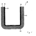
- Fig. 1 denotes an illustrative cross section of the mold for producing a silicon ingot according to the present invention.
- Fig. 2 denotes an illustrative cross section showing the solidified silicon ingot by cooling after injecting a molten silicon into the mold for producing a silicon ingot according to the present invention.
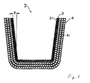
- FIG. 3 denotes an illustrative cross section of the mold for producing a silicon ingot according to the present invention.
- FIG. 4 denotes a horizontal cross section of the mold for producing a silicon ingot according to the present invention having an inner space in the mold at an arbitrary height.
- FIG. 5 denotes an illustrative cross section of the mold for producing a silicon ingot according to the present invention.
- FIG. 6 denotes an illustrative cross section showing the solidified silicon ingot by cooling after injecting a molten silicon into the mold for producing a silicon ingot according to the present invention.
- FIG. 7 denotes an illustrative cross section of the mold for producing a silicon ingot according to the present invention.
- FIG. 8 denotes an illustrative cross section showing the solidified silicon ingot by cooling after injecting a molten silicon into the mold for producing a silicon ingot according to the present invention.
- FIG. 9 denotes an illustrative cross section showing the solidified silicon ingot by cooling after injecting a molten silicon into the conventional mold for producing a silicon ingot.
- the mold 5 for producing a silicon ingot as shown in the cross section in FIG. 1 has a layered structure comprising an inner silica layer 3 containing at least one layer in which a fused silica powder (not shown in the drawing) with a particle size of 100 ⁇ m or less and a fine fused silica sand 31 with a particle size of 100 to 300 ⁇ m are bonded with a binder, and an outer silica layer 4 containing at least one layer in which a fused silica powder with a particle size of 100 ⁇ m or less and a coarse fused silica sand 41 with a particle size of 500 to 1500 ⁇ m is bonded with a silica binder.
- the inner silica layer 3 containing the fused silica sand 31 having fine particle size is readily released from the outer silica layer 4 containing silica sand 41 having coarse particle size.
- the inner silica layer 3 is released from the outer silica layer 4 by being adhered to the silicon ingot 2 when the periphery of the silicon ingot 2 is pulled toward the inner wall face of the mold as shown in FIG. 2 by shrinkage of the mold while the molten silicon poured into the cavity of the mold 5 for producing the silicon ingot is cooled after solidification. Accordingly, neither inner stress nor cracks and dislocations as seen in the ingot obtained using the conventional mold occur in the solidified silicon ingot.
- the mold for producing a silicon ingot - having a layered structure comprising an inner silica layer 3 , containing at least one layer in which the fused silica powder (not shown in the drawing) with a particle size of 100 ⁇ m or less and the fine fused silica sand 31 with a particle size of 100 to 300 ⁇ m are bonded with a binder, and an outer silica layer 4 containing at least one layer in which the fused silica powder with a particle size of 100 ⁇ m or less and the coarse fused silica sand 41 with a particle size of 500 to 1500 ⁇ m is bonded with a silica binder - is tapered from the bottom toward the opening so that the opening area becomes larger than the bottom area as shown in the cross section in FIG. 3. Because the stress generated in the silicon ingot is more reduced, a large grain size silicon ingot with few cracks and dislocations can be produced.
- the inner shape of the mold for producing the silicon ingot - having a layered structure comprising the inner silica layer 3 containing at least one layer in which the fused silica powder (not shown in the drawing) with a particle size of 100 ⁇ m or less and the fine fused silica sand 31 with a particle size of 100 to 300 ⁇ m are bonded with a binder, and an outer silica layer 4 containing at least one layer in which the fused silica powder with a particle size of 100 ⁇ m or less and the coarse fused silica sand 41 with a particle size of 500 to 1500 ⁇ m is bonded with a silica binder - may have not only a circular cross section but also a polygonal cross section.
- a used fused silica sand or a low purity fused silica sand may be used.
- the released silica sand Since the released silica sand has a smaller specific gravity than the molten silicon, the former is released to outside as SiO gas by reacting with the molten silicon after floating on the surface of the molten silica, leaving no defects within the silicon ingot.
- the mold for producing the silicon ingot has a layered structure comprising an inner silica layer containing at least one layer in which a fused silica powder with a particle size of 100 ⁇ m or less and a fine fused silica sand with a particle size of 100 to 300 ⁇ m is bonded with a silica binder, and an outer silica layer containing at least one layer in which a fused silica powder with a particle size of 100 ⁇ m or less and a coarse fused silica sand with a particle size of 500 to 1500 ⁇ m is bonded with a silica binder.
- the wall face of the inner shape of the mold for producing a silicon ingot is tapered from the bottom to the opening so that the opening area becomes larger than the bottom area.
- the mold for producing a silicon ingot has an inner space whose horizontal cross section assumes a circle or a polygon.
- the wall face of the inner shape of the mold for producing a silicon ingot is tapered from the bottom toward the opening so that the opening area becomes larger than the bottom area and the mold has an inner space whose horizontal cross section assumes a circle or a polygon.
- the method for fabricating a mold for producing a silicon ingot, based on the concept as hitherto described, having an inner silica layer and an outer silica layer comprises the steps of:
- the method for fabricating a mold for producing a silicon ingot having an inner silica layer and an outer silica layer comprises the steps of:
- the wall face of the wax mold is tapered from the bottom toward the top so that the top area becomes larger than the bottom area.
- the wall face of the wax mold is tapered from the bottom toward the top so that the top area becomes larger than the bottom area and the wax mold has a horizontal cross section assuming a circle or a polygon.
- the particle size of the fused silica sand contained in the inner layer of the mold for producing a silicon ingot according to the present invention was limited to 100 ⁇ m or less because the fused silica powder mixed with the colloidal silica is precipitated and it becomes difficult to uniformly disperse the fused silica powder when the fused silica powder has a coarse particle size of 100 ⁇ m or more.
- the particle size of the fine fused silica sand contained in the inner silica layer is limited in the range of 100 to 300 ⁇ m because the inner silica layer becomes difficult to release from the outer silica layer when the fine silica sand has a particle size as coarse as more than 300 ⁇ m while, when the fine fused silica sand contained in the inner layer has a particle size as fine as less than 50 ⁇ m, the inner silica layer becomes so readily peeled that it is released while producing the mold.
- the particle size of the coarse fused silica sand contained in the outer silica layer of the mold for producing a silicon ingot according to the present invention is limited in the range of 500 to 1500 ⁇ m because, when the coarse fused silica sand has a particle size as coarse as more than 1500 ⁇ m, the specific gravity of the mold is decreased thereby lowering its strength while, when the coarse fused silica sand has a particle size as fine as less than 500 ⁇ m, the strength of the outer silica layer is lowered along with deteriorating detachability of the outer silica layer from the inner silica layer.
- the mold for producing the silicon ingot according to the present invention has a layered structure comprising an inner silica layer containing at least one layer in which a fused silica powder with a particle size of 100 ⁇ m or less and a fine fused silica sand with a particle size of 100 to 300 ⁇ m is bonded with a silica binder, and an outer silica layer containing at least one layer in which a fused silica powder with a particle size of 100 ⁇ m or less and a coarse fused silica sand with a particle size of 500 to 1500 ⁇ m is bonded with a silica binder.
- the taper angle ⁇ is preferably in the range of 1 to 5°.
- the inner silica layer containing at least one layer in which a fused silica powder with a particle size of 100 ⁇ m or less and a fine fused silica sand with a particle size of 100 to 300 ⁇ m is bonded with a silica binder, has a thickness that allows the inner silica layer to be released by shrinking of the silicon ingot during solidification.
- the preferable thickness is in the range of 0.1 to 5 mm.
- the outer silica layer containing at least one layer in which the fused silica powder with a particle size of 100 ⁇ m or lass and the coarse fused silica sand with a particle size of 500 to 1500 ⁇ m are bonded with a binder, is required to have a thickness of about 5 mm for maintaining the strength of the mold in producing the silicon ingot.
- the practical thickness is preferably in the range of 3 to 20 mm.
- the inner silica layer of the mold for producing the ingot according to the present invention is formed by forming a slurry layer on the surface of a wax mold by dipping, followed by lifting up, a wax mold having the same shape as that of the inner shape of the mold for producing a silicon ingot into a slurry comprising a fused silica powder and colloidal silica, at least one layer of the inner stucco layer being formed by applying at least one process for forming the inner stucco layer by sprinkling the fine fused silica sand with a particle size of 100 to 300 ⁇ m on the surface of the slurry layer.
- the outer silica layer of the mold for producing the ingot according to the present invention is formed by forming at least one outer stucco layer on the inner stucco layer by applying at least one process for forming an outer stucco layer by sprinkling the coarse fused silica sand with a particle size of 500 to 1500 ⁇ m on the surface of the slurry layer after forming the slurry layer by further dipping, followed by lifting up, the wax mold on which the inner stucco layer has been formed with a slurry comprising the fused silica powder and colloidal silica.
- Inner shape of the mold for producing the silicon ingot according to the present invention can be not only fabricated to be conventional circle but also to be polygonal in the horizontal cross section at an arbitrary height of the mold for producing the silicon ingot as shown in FIG. 4.
- the mold for producing the silicon ingot according to the present invention having a space with an arbitrary size and shape of the mold is fabricated through the steps comprising: fabricating a wax mold having an arbitrary size and shape (for example, a circular column, a hexagonal column, a cube and a rectangular column); forming a slurry layer on the surface of the wax mold by dipping, followed by lifting up, the wax mold into a slurry comprising a fused silica powder with a particle size of 100 ⁇ m or less and a colloidal silica; sprinkling a fine fused silica sand with a particle size of 100 to 300 ⁇ m on the surface of the slurry layer; forming an inner silica layer by applying at least one process for forming an outer stucco layer; forming a surface slurry layer of the inner silica layer by dipping, followed by lifting up, the wax mold (having
- Inner shape of the silicon ingot having a square or rectangular cross section can be obtained by using the mold for producing the silicon ingot with a cubic or rectangular column inner space according to the present invention.
- Using the silicon ingot having a square or rectangular cross section especially for producing a square or rectangular silicon substrate of the photovoltaic solar cell allows the expensive silicon ingot to be effectively utilized.
- a silicon disk is firstly produced from the rod-shaped silicon ingot followed by cutting four corners off the silicon disk to form into a square or rectangular silicon substrate for the photovoltaic solar cell, wasting the cut-off portions from the disk.
- the silicon plate obtained by slicing the silicon ingot also has a square or rectangular shape, thereby extremely saving the cut-off proportion for producing the square or rectangular silicon substrate for the photovoltaic solar cell enabling to save the production cost.
- a cheap graphite mold or quartz mold may be used as an outermost core of the mold.
- the foregoing inner silica layer or a layer comprising the inner silica layer and outer silica layer may be used as an inner layer on the inner face of the graphite mold or quartz mold.
- the silicon ingot produced by using a graphite ingot 11 whose inner side is coated with an inner silica layer 3 containing the fused silica powder (not shown in the drawing) with a particle size of 100 pm or less and the fine fused silica sand 31 with a particle size of 100 to 300 ⁇ m, has a purity comparable to the purity of the silicon ingot produced by using the quartz mold, making it possible to obtain a silicon ingot using the graphite ingot having a photovoltaic conversion efficiency as excellent as that of the silicon ingot produced by using a quartz mold.
- the inner silica layer 3 containing the fine fused silica sand 31 is readily released from the inner wall of the graphite mold 11 in the mold for producing the silicon ingot having the inner silica layer 3 as shown by the cross section in FIG. 5. Accordingly, a peeled portion B appears as shown in the cross section in FIG. 6 by allowing the periphery of the silicon ingot 2 to be pulled by the inner wall of the mold when the solidified silicon ingot shrinks by cooling after the molten silicon is poured into the mold for producing the silicon ingot, thereby leaving no inner stress in the silicon ingot 2 . Accordingly, the ingot produced as described above never suffers from cracks due to stress as seen in the ingot produced by using a conventional quartz ingot.
- the outer silica layer 4 containing the coarse fused silica sand 41 is readily released from the inner wall of the graphite mold for producing the silicon ingot having the inner silica layer 3 and outer silica layer 4 as described above. Accordingly, a peeled portion B appears as shown in the cross section in FIG. 8 by allowing the periphery of the silicon ingot 2 to be pulled by the inner wall of the mold when the solidified silicon ingot shrinks by cooling after the molten silicon is poured into the mold for producing the silicon ingot, thereby leaving no inner stress in the silicon ingot 2 .
- Both the thicknesses of the inner silica layer and outer silica layer described above may be formed in the range as thin as 1.0 to 5.0 mm since the graphite mold serves as a reinforce core.
- a quartz mold may be used instead of the graphite mold.
- the silica sand Since the separated silica sand has smaller specific gravity than the molten silicon, the silica sand is discharged to outside as SiO gas by reacting with the molten silicon after being separated into the surface of the molten liquid, leaving no defects in the ingot behind.
- the present invention based on the findings as described above provides a mold for producing a silicon ingot in which an inner silica layer containing fine fused silica sand with a particle size of 100 to 300 ⁇ m is formed on the inner surface of a graphite mold or quartz mold.
- the present invention also provides a mold for producing a silicon ingot in which an inner silica layer containing at least one layer prepared by binding fused silica powder with a particle size of 100 ⁇ m or less with fine fused silica sand with a particle size of 100 to 300 ⁇ m is formed on the inner surface of a graphite mold or quartz mold.
- the present invention also provides a mold for producing a silicon ingot in which an outer silica layer containing coarse fused silica sand with a particle size of 500 to 1500 ⁇ m is formed on the inner face of a graphite mold or a quartz mold, an inner silica layer containing fine fused silica sand with a particle size of 100 to 300 ⁇ m being formed on the inner side of the outer silica layer.
- the present invention also provides a mold for producing a silicon ingot in which an outer silica layer containing at least one layer prepared by joining fused silica powder with a particle size of 100 pm or less and coarse fused silica sand with a particle size of 500 to 1500 ⁇ m with a silica binder is formed on the inner face of a graphite mold or quartz mold, an inner silica layer containing at least one layer prepared by joining fused silica powder with a particle size of 100 ⁇ m or less and fine fused silica sand with a particle size of 100 to 300 ⁇ m with a silica binder being formed on the outer silica layer.
- the present invention also provides a mold for producing a silicon ingot in which the wall face of the mold is tapered from the bottom toward the opening so that the opening area becomes larger than the bottom area.
- the present invention also provides a mold for producing a silicon ingot in which the horizontal cross section of the mold has an inner space assuming a circle or a polygon.
- the present invention also provides a mold for producing a silicon ingot in which the wall face of the mold is tapered from the bottom toward the opening so that the opening area becomes larger than the bottom area and the horizontal cross section of the mold has an inner space assuming a circle or a polygon.
- the present invention provides a method for fabricating a mold for producing a silicon ingot, wherein a stucco layer is formed by sprinkling, followed by baking, fine fused silica sand with a particle size of 100 to 300 ⁇ m on the surface of a slurry layer after forming the slurry layer on the inner face of the mold by coating or spraying the slurry comprising fused silica powder with a particle size of 100 ⁇ m or less and colloidal silica on inside of a graphite mold or a quartz mold.
- the present invention also provides a method for fabricating a mold for producing a silicon ingot comprising the steps of:
- the present invention also provides a method for fabricating a mold for producing a silicon ingot in which the inner wall face of the graphite mold or the quartz mold is tapered from the bottom toward the opening so that the opening area becomes larger than the bottom area.
- the present invention also provides a method for fabricating a mold for producing a silicon ingot in which horizontal cross section of the graphite mold or the quartz mold assumes a circle or a polygon.
- the present invention also provides a method for fabricating a mold for producing a silicon ingot in which the inner wall face of the graphite mold or the quartz mold is tapered from the bottom toward the opening so that the opening area becomes larger than the bottom area and horizontal cross section of the graphite mold or the quartz mold assumes a circle or a polygon.
- the inner silica layer of the mold for producing the silicon ingot according to the present invention can be formed by the steps comprising: forming a slurry layer on the inner surface of the quartz mold or graphite mold by coating or spraying a slurry comprising a fused silica powder with a mean particle size of 100 ⁇ m or lass and colloidal silica; and applying one or a plurality of the stucco forming process by sprinkling, followed by baking, a fine fused silica sand with a particles size of 100 to 300 ⁇ m on the inner surface of the slurry layer to form a stucco layer.
- Forming the stucco layer on the slurry coating layer comprising fused the silica powder and silica slurry by sprinkling the fine fused silica sand allows defect generation that have been appeared by coating the conventional release agent to be avoided.
- the particle size of the fused silica sand contained in the inner silica layer is limited to 100 ⁇ m or less in the mold for producing the silica ingot according to the present invention because, when the fused silica powder has a particle size as coarse as more than 100 ⁇ m, it becomes difficult to uniformly sprinkle the powder since the fused silica powder mixed with the colloidal silica is precipitated.
- the particle size of the fine fused silica sand contained in the inner silica layer is limited within the range of 100 to 300 ⁇ m because, when the fine fused silica sand has a particle size as coarse as more than 300 ⁇ m, the surface roughness of the inner silica layer becomes too large while, when the fine fused silica sand has a particle size as fine as less than 100 ⁇ m, the inner silica layer is insufficiently released from the mold as well as making it impossible to maintain a sufficient thickness.
- the mold for producing the silicon ingot according to the present invention can be also fabricated through the steps comprising: forming a slurry layer by coating or spraying a slurry comprising a fused silica powder with a particle size of 100 ⁇ m or less and a colloidal silica on the inner face of the graphite mold or quartz mold; applying one or a plurality of stucco layer forming processes by sprinkling a coarse fused silica sand with a particle size of 500 to 1500 ⁇ m on the surface of the slurry layer; forming a slurry layer by coating or spraying a slurry comprising a fused silica powder with a particle size of 100 ⁇ m or less and a colloidal silica on the inner surface of the graphite mold on the stucco layer; applying one or a plurality of stucco layer forming processes by sprinkling, followed by baking, a fine fused silica sand with a particle size of 100 to 300 ⁇ m
- a thick outer silica layer can be formed by sprinkling the coarse fused silica sand, allowing a layer comprising the outer silica layer and inner silica layer to be formed within a short period of time along with allowing the inner silica layer to be thin.
- a thick and strong outer silica layer can be more simply formed as the particle size of the coarse fused silica sand to be sprinkled on the surface of the slurry layer is larger, the surface of the outer silica layer becomes too rough when the particle size of the coarse fused silica sand contained in the outer silica layer of the mold for producing the silicon ingot is as coarse as more than 1500 ⁇ m, adversely affecting smoothness of the inner silica layer.
- a strong and thick outer silica layer can not be so easily formed.
- a wax mold with a diameter of 250 mm and a height of 100 mm was prepared.
- a binder comprising 30% by volume of super-fine fused silica powder with a particle size of 100 A or less and a balance of water (referred to a colloidal silica hereinafter) was also prepared to produce a slurry by mixing 200 parts of the colloidal silica with 200 parts of the fused silica powder with a particle size of 40 ⁇ m.
- the wax mold above was dipped into the slurry obtained, followed by lifting up, to form a slurry layer on the surface of the wax mold.
- Fine fused silica sand with a particle size of 150 ⁇ m was sprinkled on the surface of the slurry layer. This process was repeated three times to form a stucco layer, thereby forming an inner stucco layer comprising three layers with a combined thickness of 3 mm on the surface of the wax mold.
- the wax mold on the surface of which the inner stucco layer was formed was dipped into the foregoing slurry again, followed by lifting up, to form a slurry layer on the surface of the inner stucco layer of the wax mold.
- Coarse fused silica sand with a particle size of 1000 ⁇ m was sprinkled on the surface of the slurry layer and, by forming stucco layers by repeating the above process eight times, an outer stucco layer comprising eight layers with a combined thickness of 8 mm was formed on the surface of the wax mold.
- the wax mold whose inner surface was coated with the inner stucco layer and outer stucco layer was removed by allowing the wax to melt by heating at 100°C.
- the layered body obtained comprising the inner stucco layer and outer stucco layer was baked by keeping at a temperature of 800°C for 2 hours, producing a mold for producing the silicon ingot according to the present invention comprising the inner silica layer and outer silica layer (referred to a mold according to the present invention hereinafter).
- a molten silicon held at a temperature of 1500°C was poured into the mold 1 according to the present invention and was cooled at a cooling rate of 1°K/sec., producing a columnar silicon ingot by taking out the ingot from the mold 1 according to the present invention. Presence of cracks due to stress and the amount of the remaining release agent on the surface of the columnar silicon ingot obtained were visually observed. Also, the polycrystalline silicon ingot obtained was sliced to produce a silicon substrate with a width of 150 mm and a length of 150 mm for use in the photovoltaic solar cell and the photovoltaic conversion efficiency of the silicon substrate was measured. The results of the observation and measurement are summarized in TABLE 1.
- a rectangular column shaped wax mold with a length of 170 mm, a width of 170 mm and a height of 100 mm was prepared.
- the mold 2 according to the present invention was fabricated by the method as in Example 1 to produce a rectangular column shaped silicon ingot by the same method as in Example 1. Presence of cracks due to stress and the amount of the remaining release agent on the surface of the rectangular column shaped silicon ingot obtained were visually observed. Also, the polycrystalline silicon ingot obtained was sliced to produce a silicon substrate with a width of 150 mm and a length of 150 mm for use in the photovoltaic solar cell and the photovoltaic conversion efficiency of the silicon substrate was measured. The results of the observation and measurement are summarized in TABLE 1.
- a conical table shaped wax mold with a bottom diameter of 190 mm, a top diameter of 200 mm and a height of 100 mm whose side face is tapered at an angle of 3° was prepared.
- the mold 3 according to the present invention was fabricated using the conical table shaped wax mold by the method as in Example 1 to produce a conical table shaped silicon ingot by the same method as in Example 1. Presence of cracks due to stress and the amount of the remaining release agent on the surface of the rectangular column shaped silicon ingot obtained were visually observed. Also, the polycrystalline silicon ingot obtained was sliced to produce a silicon substrate with a width of 150 mm and a length of 150 mm for use in the photovoltaic solar cell and the photovoltaic conversion efficiency of the silicon substrate was measured. The results of the observation and measurement are summarized in TABLE 1.
- a graphite mold with an inner width of 170 mm and inner length of 170 mm, an outer width of 190 mm and outer length of 190 mm, and a depth of 150 mm was prepared.
- Colloidal silica comprising 30% by volume of super-fine fused silica powder and a balance of water was also prepared.
- a slurry was formed by mixing 100 parts of this colloidal silica with 200 parts of fused silica powder having a mean particle size of 40 ⁇ m.
- a slurry layer was formed by coating the inner face of the graphite mold with the slurry obtained, followed by forming a stucco layer by sprinkling the fine fused silica sand with a particle size of 150 ⁇ m on the surface of the slurry layer. This process was repeated three times and an inner silica layer with a combined thickness of 2 mm was formed on the inner face of the graphite mold by baking at a temperature of 800°C for two hours, thereby fabricating the mold 4 according to
- a molten silicon kept at a temperature of 1500°C was poured into the mold 4 according to the present invention to produce a polycrystalline silicon ingot. Presence of cracks due to stress and the amount of the remaining release agent on the surface of the polycrystalline silicon ingot obtained were visually observed. Also, the polycrystalline silicon ingot obtained was sliced to produce a silicon substrate with a width of 150 mm and a length of 150 mm for use in the photovoltaic solar cell and the photovoltaic conversion efficiency of the silicon substrate was measured. The results of the observation and measurement are summarized in TABLE 1.
- a slurry layer was formed using the graphite mold and slurry prepared in Example 4 by coating the inner face of the graphite mold with the slurry.
- the coarse fused silica sand with a particle size of 1000 ⁇ m was sprinkled on the surface of the slurry layer to form a stucco layer by repeating this sprinkle process twice.
- a slurry layer was additionally formed by coating the surface of the stucco layer with the slurry prepared in Example 4.
- the fine fused silica sand with a particle size of 150 ⁇ m was sprinkled on the slurry layer to form a stucco layer by repeating this sprinkle process twice, thereby forming a stucco layer containing coarse fused silica sand and fine fused silica sand.
- the graphite mold in which the stucco layer was formed was baked at a temperature of 800°C for 8 hours in an inert gas atmosphere, fabricating the mold 5 according to the present invention by forming a layer comprising the inner silica layer and outer silica layer with a combined thickness of 3 mm on the inner face of the graphite mold.
- a molten silicon kept at a temperature of 1500°C was poured into the mold 5 according to the present invention and the mold was cooled at a cooling rate of 0.6°C/sec, to produce a polycrystalline silicon ingot. Presence of cracks due to stress and the amount of the remaining release agent on the surface of the polycrystalline silicon ingot obtained were visually observed. Also, the polycrystalline silicon ingot obtained was sliced to produce a silicon substrate with a width of 150 mm and a length of 150 mm for use in the photovoltaic solar cell and the photovoltaic conversion efficiency of the silicon substrate was measured. The results of the observation and measurement are summarized in TABLE 1.
- a mold prepared by coating Si 3 N 4 on the inner face of the graphite mold as prepared in Example 4 was used as a conventional graphite mold.
- a molten silicon kept at a temperature of 1500°C the molten silicon prepared in Example 4 was poured into the conventional graphite mold and the mold was cooled at a cooling rate of 0.6°C/sec., producing a polycrystalline silicon ingot by taking the silicon ingot out of the conventional graphite mold. Presence of cracks due to stress and the amount of the remaining release agent on the surface of the polycrystalline silicon ingot obtained were visually observed.
- the polycrystalline silicon ingot obtained was sliced to produce a silicon substrate with a width of 150 mm and a length of 150 mm for use in the photovoltaic solar cell and the photovoltaic conversion efficiency of the silicon substrate was measured.
- the results of the observation and measurement are summarized in TABLE 1.
- a conventional quartz mold with an inner diameter of 240 mm, an outer diameter of 250 mm and a depth of 150 mm were prepared.
- the polycrystalline silicon ingot obtained was sliced to produce a silicon substrate with a width of 150 mm and a length of 150 mm for use in the photovoltaic solar cell and the photovoltaic conversion efficiency of the silicon substrate was measured.
- the results of the observation and measurement are summarized in TABLE 1.
- Kind of mold Stress Cracks Residual release agent Photovoltaic conversion efficiency (%) Mold 1 of the present invention Non Non 14.2 Mold 2 of the present invention Non Non 13.9 Mold 3 of the present invention Non Non 14.1 Mold 4 of the present invention Non Non 13.9 Mold 5 of the present invention Non Non 14.0 Conventional graphite mold Non Yes 12.8 Conventional quartz mold Yes Non 14.2
- the polycrystalline silicon ingot produced by using the molds 1 to 5 according to the present invention has a better photovoltaic conversion efficiency then the polycrystalline silicon ingot using the conventional graphite mold.
- the polycrystalline silicon ingot produced by using the molds 1 to 5 according to the present invention has a photovoltaic conversion efficiency comparable to the polycrystalline silicon ingot produced by using the conventional quartz mold, using the mold 1 to 5 according to the present invention allows production yield of the polycrystalline silicon ingot to be high, being free from the residual release agent.
- the present invention provides a mold for producing a silicon ingot with which a polycrystalline silicon ingot having a good photovoltaic conversion efficiency, being free from the residual release agent and generating no cracks due to stress can be produced.
- a silicon ingot having not only a circular cross section but also a polygonal cross section is produce, a square or rectangular silicon substrate such as a silicon substrate for use in the photovoltaic solar cell can be produced with no waste of the silicon ingot, being effective for mass production and cost down of the silicon substrate for use in the photovoltaic solar cell.
Landscapes
- Chemical & Material Sciences (AREA)
- Engineering & Computer Science (AREA)
- Crystallography & Structural Chemistry (AREA)
- Materials Engineering (AREA)
- Metallurgy (AREA)
- Organic Chemistry (AREA)
- Silicon Compounds (AREA)
- Mold Materials And Core Materials (AREA)
Abstract
Description
| Kind of mold | Stress Cracks | Residual release agent | Photovoltaic conversion efficiency (%) |
| Mold 1 of the present invention | Non | Non | 14.2 |
| | Non | Non | 13.9 |
| | Non | Non | 14.1 |
| | Non | Non | 13.9 |
| Mold 5 of the present invention | Non | Non | 14.0 |
| Conventional graphite mold | Non | Yes | 12.8 |
| Conventional quartz mold | Yes | Non | 14.2 |
Claims (21)
- A mold for producing a silicon ingot having a layered structure comprising an inner silica layer containing at least one layer in which a fused silica powder with a particle size of 100 µm or less and a fine fused silica sand with a particle size of 100 to 300 µm is bonded with a silica binder, and an outer silica layer containing at least one layer in which a fused silica powder with a particle size of 100 µm or less and a coarse fused silica sand with a particle size of 500 to 1500 µm is bonded with a silica binder.
- A mold for producing a silicon ingot according to Claim 1, wherein the wall face of the inner shape of the mold for producing a silicon ingot is tapered from the bottom toward the opening so that the opening area becomes larger than the bottom area.
- A mold for producing a silicon ingot according to Claim 1 having an inner space whose horizontal cross section assumes a circle or a polygon.
- A mold for producing a silicon ingot according to Claim 1, wherein the wall face of the inner shape of the mold for producing a silicon ingot is tapered from the bottom toward the opening so that the opening area becomes larger than the bottom area and the mold has an inner space whose horizontal cross section assumes a circle or a polygon.
- A method for fabricating a mold for producing a silicon ingot having an inner silica layer and an outer silica layer comprising the steps of:forming a slurry layer on the surface of a wax mold by dipping, followed by lifting up, the wax mold having the same shape as that of the inner shape of the mold for producing a silicon ingot into a slurry comprising a fused silica powder and colloidal silica, followed by forming an inner stucco layer by sprinkling a fine fused silica sand with a particle size of 100 to 300 µm on the surface of the slurry layer;forming an outer stucco layer on the inner stucco layer by sprinkling coarse fused silica sand with a particle size of 500 to 1500 µm on the surface of the slurry layer after forming the slurry layer by further dipping, followed by lifting up, the wax mold on which the inner stucco layer has been formed into a slurry comprising the fused silica powder and colloidal silica; andheat-melting and eliminating the wax mold along with baking the inner stucco layer and outer stucco layer.
- A method for fabricating a mold for producing a silicon ingot having an inner silica layer and an outer silica layer comprising the steps of:forming a slurry layer on the surface of a wax mold by dipping, followed by lifting up, a wax mold having the same shape as that of the inner shape of the mold for producing a silicon ingot by dipping into a slurry comprising a fused silica powder and colloidal silica, at least one layer of an inner stucco layer being formed by applying at least one process for forming the inner stucco layer by sprinkling a fine fused silica sand with a particle size of 100 to 300 µm on the surface of the slurry layer;forming at least one outer stucco layer on the inner stucco layer by applying at least one process for forming an outer stucco layer by sprinkling the coarse fused silica sand with a particle size of 500 to 1500 µm on the surface of the slurry layer after forming the slurry layer by further dipping, followed by lifting up, the wax mold on which the inner stucco layer has been formed into a slurry comprising the fused silica powder and colloidal silica; andheat-melting and eliminating the wax mold along with baking the inner stucco layer and outer stucco layer.
- A method for fabricating a mold for producing a silicon ingot according to Claim 5 or 6, wherein the inner wall face of the wax mold is tapered from the bottom toward the top so that the top area becomes larger than the bottom area.
- A method for fabricating a mold for producing a silicon ingot according to Claim 5 or 6, wherein the wax mold has a horizontal cross section assuming a circle or a polygon.
- A method for fabricating a mold for producing a silicon ingot according to Claim 5 or 6, wherein the inner wall face of the wax mold is tapered from the bottom toward the top so that the top area becomes larger than the bottom area and the wax mold has a horizontal cross section assuming a circle or a polygon.
- A mold for producing a silicon ingot in which an inner silica layer containing a fine fused silica sand with a particle size of 100 to 300 µm is formed on the inner surface of a graphite mold or quartz mold.
- A mold for producing a silicon ingot in which an inner silica layer containing at least one layer prepared by binding a fused silica powder with a particle size of 100 µm or less and fine fused silica sand with a particle size of 100 to 300 µm with a silica binder is formed on the inner surface of a graphite mold or quartz mold.
- A mold for producing a silicon ingot in which an outer silica layer containing a coarse fused silica sand with a particle size of 500 to 1500 µm is formed on the inner face of a graphite mold or a quartz mold, an inner silica layer containing a fine fused silica sand with a particle size of 100 to 300 µm being formed on the inner side of the outer silica layer.
- A mold for producing a silicon ingot in which an outer silica layer containing at least one layer prepared by joining fused silica powder with a particle size of 100 µm or less and coarse fused silica sand with a particle size of 500 to 1500 µm with a silica binder is formed on the inner face of a graphite mold or quartz mold, an inner silica layer containing at least one layer prepared by joining the fused silica powder with a particle size of 100 µm or less and fine fused silica sand with a particle size of 100 to 300 µm with a silica binder being formed on the outer silica layer.
- A mold for producing a silicon ingot according to Claim 10, 11, 12 or 13, wherein the inner wall face of the mold for producing a silicon ingot is tapered from the bottom toward the opening so that the opening area becomes larger than the bottom area.
- A mold for producing a silicon ingot according to Claim 10, 11, 12 or 13, wherein the horizontal cross section of the mold for producing a silicon ingot has an inner space assuming a circle or a polygon.
- A mold for producing a silicon ingot according to Claim 10, 11, 12 or 13, wherein the inner wall face of the mold for producing a silicon ingot is tapered from the bottom toward the opening so that the opening area becomes larger than the bottom area and the horizontal cross section of the mold has an inner space assuming a circle or a polygon.
- A method for fabricating a mold for producing a silicon ingot, wherein a stucco layer is formed by sprinkling, followed by baking, a fine fused silica sand with a particle size of 100 to 300 µm on the surface of a slurry layer after forming the slurry layer on the inner face of the graphite mold or the quartz mold by coating or spraying the slurry comprising fused silica powder with a particle size of 100 µm or less and colloidal silica.
- A method for fabricating a mold for producing a silicon ingot comprising the steps of:forming an outer stucco layer by sprinkling a coarse fused silica sand with a particle size of 500 to 1500 µm on the surface of a slurry layer after forming the slurry layer on the inner face of the mold by coating or spraying a slurry comprising the fused silica powder with a particle size of 100 µm or less and colloidal silica on the inner side of a graphite mold or a quartz mold; andforming a stucco layer by sprinkling, followed by baking, a fine fused silica sand with a particle size of 100 to 300 µm on the surface of the slurry layer after forming the slurry layer by further coating or spraying the slurry comprising fused the silica powder with a particle size of 100 µm or less and colloidal silica on the outer stucco layer.
- A method for fabricating a mold for producing a silicon ingot according to Claim 17 or 18, wherein the inner wall face of the graphite mold or the quartz mold is tapered from the bottom toward the opening so that the opening area becomes larger than the bottom area.
- A method for fabricating a mold for producing a silicon ingot according to Claim 17 or 18, wherein horizontal cross section of the graphite mold or the quartz mold assumes a circle or a polygon.
- A method for fabricating a mold for producing a silicon ingot according to Claim 17 or 18, wherein the inner wall face of the graphite mold or the quartz mold is tapered from the bottom toward the opening so that the opening area becomes larger than the bottom area and horizontal cross section of the graphite mold or the quartz mold assumes a circle or a polygon.
Applications Claiming Priority (4)
| Application Number | Priority Date | Filing Date | Title |
|---|---|---|---|
| JP4546098 | 1998-02-26 | ||
| JP4546098A JP3206540B2 (en) | 1998-02-26 | 1998-02-26 | Laminated crucible for producing silicon ingot and method for producing the same |
| JP4744998 | 1998-02-27 | ||
| JP04744998A JP3250149B2 (en) | 1998-02-27 | 1998-02-27 | Silicon ingot casting mold and method of manufacturing the same |
Publications (3)
| Publication Number | Publication Date |
|---|---|
| EP0949358A2 true EP0949358A2 (en) | 1999-10-13 |
| EP0949358A3 EP0949358A3 (en) | 2002-01-02 |
| EP0949358B1 EP0949358B1 (en) | 2003-11-12 |
Family
ID=26385451
Family Applications (1)
| Application Number | Title | Priority Date | Filing Date |
|---|---|---|---|
| EP99103701A Expired - Lifetime EP0949358B1 (en) | 1998-02-26 | 1999-02-25 | Mold for producing silicon ingot and method for fabricating the same |
Country Status (3)
| Country | Link |
|---|---|
| US (2) | US6334603B1 (en) |
| EP (1) | EP0949358B1 (en) |
| DE (1) | DE69912668T2 (en) |
Cited By (10)
| Publication number | Priority date | Publication date | Assignee | Title |
|---|---|---|---|---|
| WO2009014962A1 (en) * | 2007-07-20 | 2009-01-29 | Bp Corporation North America Inc. | Methods and apparatuses for manufacturing cast silicon from seed crystals |
| US8048221B2 (en) | 2006-01-20 | 2011-11-01 | Stoddard Nathan G | Methods and apparatuses for manufacturing monocrystalline cast silicon and monocrystalline cast silicon bodies for photovoltaics |
| EP2589687A1 (en) * | 2011-11-04 | 2013-05-08 | Vesuvius France (S.A.) | Crucible and method for the production of a (near ) monocrystalline semiconductor ingot |
| US8591649B2 (en) | 2007-07-25 | 2013-11-26 | Advanced Metallurgical Group Idealcast Solar Corp. | Methods for manufacturing geometric multi-crystalline cast materials |
| CN103635614A (en) * | 2011-04-25 | 2014-03-12 | 康宁股份有限公司 | Vessels for molten semiconducting materials and methods of making the same |
| CN104389014A (en) * | 2014-12-02 | 2015-03-04 | 江苏科技大学 | Quartz crucible for single crystal growth and preparation method of quartz crucible for single crystal growth |
| EP2982780A1 (en) | 2014-08-04 | 2016-02-10 | Heraeus Quarzglas GmbH & Co. KG | Mould made of quartz glass or quartz and method for the preparation of same |
| CN106521621A (en) * | 2016-09-20 | 2017-03-22 | 江西赛维Ldk太阳能高科技有限公司 | Ingot casting method capable of reducing red edge width of polycrystalline silicon ingot, polycrystalline silicon ingot and crucible for polycrystalline silicon ingot casting |
| WO2017199132A1 (en) * | 2016-05-18 | 2017-11-23 | Rec Solar Pte. Ltd. | Silicon ingot growth crucible with patterned protrusion structured layer |
| CN108188361A (en) * | 2017-12-01 | 2018-06-22 | 重庆材料研究院有限公司 | A kind of method for preventing high temperature alloy from melting adhesion pedestal when pouring into a mould |
Families Citing this family (20)
| Publication number | Priority date | Publication date | Assignee | Title |
|---|---|---|---|---|
| US6491971B2 (en) * | 2000-11-15 | 2002-12-10 | G.T. Equipment Technologies, Inc | Release coating system for crucibles |
| DE102005050593A1 (en) * | 2005-10-21 | 2007-04-26 | Esk Ceramics Gmbh & Co. Kg | Skim coat for making a durable hard coating on substrates, e.g. crucibles for melt-processing silicon, comprises silicon nitride particles and a binder consisting of solid nano-particles made by a sol-gel process |
| JP2007332022A (en) * | 2006-06-13 | 2007-12-27 | Young Sang Cho | Apparatus for producing polycrystalline silicon ingot |
| EP2058279A4 (en) * | 2006-08-31 | 2012-01-25 | Mitsubishi Materials Corp | METAL SILICON AND METHOD FOR MANUFACTURING THE SAME |
| NO327122B1 (en) * | 2007-03-26 | 2009-04-27 | Elkem Solar As | A composition |
| JP2010534189A (en) * | 2007-07-20 | 2010-11-04 | ビーピー・コーポレーション・ノース・アメリカ・インコーポレーテッド | Method and apparatus for producing cast silicon from seed crystals |
| WO2009015167A1 (en) | 2007-07-25 | 2009-01-29 | Bp Corporation North America Inc. | Methods for manufacturing monocrystalline or near-monocrystalline cast materials |
| US8945316B2 (en) * | 2008-02-07 | 2015-02-03 | Fontana Technology | Method for shaping and slicing ingots using an aqueous phosphate solution |
| TW201012978A (en) * | 2008-08-27 | 2010-04-01 | Bp Corp North America Inc | Apparatus and method of use for a casting system with independent melting and solidification |
| JP5102744B2 (en) * | 2008-10-31 | 2012-12-19 | ジャパンスーパークォーツ株式会社 | Quartz crucible mold |
| US8859034B2 (en) * | 2009-01-28 | 2014-10-14 | Kyocera Corporation | Ingot mold for silicon ingot and method for making the same |
| DE102010000687B4 (en) | 2010-01-05 | 2012-10-18 | Solarworld Innovations Gmbh | Crucible and method for producing silicon blocks |
| DE102011004753A1 (en) * | 2011-02-25 | 2012-08-30 | Evonik Degussa Gmbh | Process for purifying silicon |
| JP5519869B2 (en) * | 2011-09-05 | 2014-06-11 | ポリプラスチックス株式会社 | Mold |
| DE102011082628B4 (en) * | 2011-09-13 | 2018-10-04 | Fraunhofer-Gesellschaft zur Förderung der angewandten Forschung e.V. | Apparatus and method for producing silicon blocks |
| JP6014336B2 (en) * | 2012-02-28 | 2016-10-25 | シャープ株式会社 | Silicon casting mold, silicon casting method, silicon material manufacturing method, and solar cell manufacturing method |
| CN108624956A (en) * | 2018-06-12 | 2018-10-09 | 山东大海新能源发展有限公司 | Polysilicon fine melt casting ingot process |
| CN108588829B (en) * | 2018-06-12 | 2020-10-27 | 山东大海新能源发展有限公司 | Polycrystalline silicon full-melting ingot casting process and crucible used by same |
| CN114315320B (en) * | 2021-12-29 | 2023-03-24 | 耐镁佳(营口)金属有限公司 | Magnesium oxide refractory material and application thereof |
| JP2024145345A (en) * | 2023-03-31 | 2024-10-15 | 三菱マテリアル電子化成株式会社 | Silicon ingot, crucible for producing silicon ingot, method for producing crucible for producing silicon ingot, and method for producing silicon ingot |
Family Cites Families (9)
| Publication number | Priority date | Publication date | Assignee | Title |
|---|---|---|---|---|
| GB1107454A (en) * | 1964-06-22 | 1968-03-27 | Sandvikens Jernverks Ab | Improvements in or relating to bottom bricks or plugs for ingot moulds |
| US3396935A (en) * | 1965-08-27 | 1968-08-13 | Nalco Chemical Co | Metal ingot mold with protective coating |
| DE2009459A1 (en) * | 1970-02-28 | 1971-09-09 | Consortium Elektrochem Ind | Process for the production of Sihciumformkorpern |
| FR2345253A1 (en) * | 1976-03-23 | 1977-10-21 | Radiotechnique Compelec | Crucible for mfg. monocrystalline gallium arsenide - using mat on crucible wall to prevent dislocations |
| US4683937A (en) * | 1977-03-04 | 1987-08-04 | United States Steel Corporation | Ingot mold and method of producing same |
| US4548381A (en) * | 1984-09-05 | 1985-10-22 | Solarex Corporation | Castable receiver |
| EP0204674B1 (en) * | 1985-06-06 | 1991-12-27 | Remet Corporation | Casting of reactive metals into ceramic molds |
| US5389582A (en) * | 1985-11-06 | 1995-02-14 | Loxley; Ted A. | Cristobalite reinforcement of quartz glass |
| JP2933404B2 (en) * | 1990-06-25 | 1999-08-16 | 信越石英 株式会社 | Quartz glass crucible for pulling silicon single crystal and its manufacturing method |
-
1999
- 1999-02-25 EP EP99103701A patent/EP0949358B1/en not_active Expired - Lifetime
- 1999-02-25 DE DE69912668T patent/DE69912668T2/en not_active Expired - Lifetime
- 1999-02-26 US US09/258,821 patent/US6334603B1/en not_active Expired - Lifetime
-
2001
- 2001-08-24 US US09/935,549 patent/US6732992B2/en not_active Expired - Lifetime
Cited By (23)
| Publication number | Priority date | Publication date | Assignee | Title |
|---|---|---|---|---|
| US8628614B2 (en) | 2006-01-20 | 2014-01-14 | Amg Idealcast Solar Corporation | Methods and apparatus for manufacturing monocrystalline cast silicon and monocrystalline cast silicon bodies for photovoltaics |
| US8951344B2 (en) | 2006-01-20 | 2015-02-10 | Amg Idealcast Solar Corporation | Methods and apparatuses for manufacturing geometric multicrystalline cast silicon and geometric multicrystalline cast silicon bodies for photovoltaics |
| US8048221B2 (en) | 2006-01-20 | 2011-11-01 | Stoddard Nathan G | Methods and apparatuses for manufacturing monocrystalline cast silicon and monocrystalline cast silicon bodies for photovoltaics |
| US8440157B2 (en) | 2007-07-20 | 2013-05-14 | Amg Idealcast Solar Corporation | Methods and apparatuses for manufacturing cast silicon from seed crystals |
| WO2009014962A1 (en) * | 2007-07-20 | 2009-01-29 | Bp Corporation North America Inc. | Methods and apparatuses for manufacturing cast silicon from seed crystals |
| US20100197070A1 (en) * | 2007-07-20 | 2010-08-05 | BP Corproation North America Inc. | Methods and Apparatuses for Manufacturing Cast Silicon From Seed Crystals |
| US8591649B2 (en) | 2007-07-25 | 2013-11-26 | Advanced Metallurgical Group Idealcast Solar Corp. | Methods for manufacturing geometric multi-crystalline cast materials |
| CN103635614A (en) * | 2011-04-25 | 2014-03-12 | 康宁股份有限公司 | Vessels for molten semiconducting materials and methods of making the same |
| WO2013064626A1 (en) | 2011-11-04 | 2013-05-10 | Vesuvius France Sa | Crucible and method for the production of a (near) monocrystalline semiconductor ingot |
| EP2589687A1 (en) * | 2011-11-04 | 2013-05-08 | Vesuvius France (S.A.) | Crucible and method for the production of a (near ) monocrystalline semiconductor ingot |
| CN104040038A (en) * | 2011-11-04 | 2014-09-10 | 维苏威法国股份有限公司 | Crucible and method for the production of a (near) monocrystalline semiconductor ingot |
| CN104040038B (en) * | 2011-11-04 | 2016-11-02 | 维苏威法国股份有限公司 | Crucible and the production method of (closely) single crystal semiconductor ingot |
| EP2982780A1 (en) | 2014-08-04 | 2016-02-10 | Heraeus Quarzglas GmbH & Co. KG | Mould made of quartz glass or quartz and method for the preparation of same |
| CN105316761A (en) * | 2014-08-04 | 2016-02-10 | 赫罗伊斯石英玻璃股份有限两合公司 | Silicon block, method for producing same, crucible of transparent or opaque fused silica suited for performing the method, and method for production thereof |
| US9828691B2 (en) | 2014-08-04 | 2017-11-28 | Heraes Quarzglas GmbH & Co. KG | Silicon block, method for producing the same, crucible of transparent or opaque fused silica suited for performing the method, and method for the production thereof |
| CN105316761B (en) * | 2014-08-04 | 2018-09-14 | 赫罗伊斯石英玻璃股份有限两合公司 | Silico briquette, its production method, be adapted for carrying out this method transparent or opaque fused silica crucible and its production method |
| CN104389014A (en) * | 2014-12-02 | 2015-03-04 | 江苏科技大学 | Quartz crucible for single crystal growth and preparation method of quartz crucible for single crystal growth |
| CN104389014B (en) * | 2014-12-02 | 2017-04-05 | 江苏科技大学 | A kind of silica crucible for crystal growth and preparation method thereof |
| WO2017199132A1 (en) * | 2016-05-18 | 2017-11-23 | Rec Solar Pte. Ltd. | Silicon ingot growth crucible with patterned protrusion structured layer |
| CN106521621A (en) * | 2016-09-20 | 2017-03-22 | 江西赛维Ldk太阳能高科技有限公司 | Ingot casting method capable of reducing red edge width of polycrystalline silicon ingot, polycrystalline silicon ingot and crucible for polycrystalline silicon ingot casting |
| CN106521621B (en) * | 2016-09-20 | 2019-01-29 | 江西赛维Ldk太阳能高科技有限公司 | A kind of casting ingot method, polycrystal silicon ingot and crucible used for polycrystalline silicon ingot casting reducing the red hem width degree of polycrystal silicon ingot |
| CN108188361A (en) * | 2017-12-01 | 2018-06-22 | 重庆材料研究院有限公司 | A kind of method for preventing high temperature alloy from melting adhesion pedestal when pouring into a mould |
| CN108188361B (en) * | 2017-12-01 | 2020-05-01 | 重庆材料研究院有限公司 | Method for preventing base from being fused and adhered during high-temperature alloy pouring |
Also Published As
| Publication number | Publication date |
|---|---|
| US6334603B1 (en) | 2002-01-01 |
| US20020014574A1 (en) | 2002-02-07 |
| DE69912668T2 (en) | 2004-09-30 |
| EP0949358B1 (en) | 2003-11-12 |
| DE69912668D1 (en) | 2003-12-18 |
| EP0949358A3 (en) | 2002-01-02 |
| US6732992B2 (en) | 2004-05-11 |
Similar Documents
| Publication | Publication Date | Title |
|---|---|---|
| EP0949358B1 (en) | Mold for producing silicon ingot and method for fabricating the same | |
| KR101779267B1 (en) | Polycrystalline silicon ingot, method for producing the same, and crucible | |
| US20060057317A1 (en) | Vessel for holding silicon and method of producing the same | |
| JP3931322B2 (en) | Silicon ingot casting mold and manufacturing method thereof | |
| US20040211496A1 (en) | Reusable crucible for silicon ingot growth | |
| KR20120055592A (en) | Composite crucible, method for producing same, and method for producing silicon crystal | |
| US20130015318A1 (en) | Layered crucible for casting silicon ingot and method of producing same | |
| EP3458629B1 (en) | Silicon ingot growth crucible with patterned protrusion structured layer | |
| CN106801252A (en) | A kind of quartz ceramic crucible for polycrystalline silicon ingot casting and preparation method thereof | |
| CN104671670A (en) | Method For Producing A Coated Component Of Quartz Glass Or Fused Silica | |
| US20130192302A1 (en) | Crucibles for holding molten material and methods for producing them and for their use | |
| JP3206540B2 (en) | Laminated crucible for producing silicon ingot and method for producing the same | |
| JP3250149B2 (en) | Silicon ingot casting mold and method of manufacturing the same | |
| CN106278302B (en) | A kind of preparation technology of gradient high-purity fused silica crucible | |
| CN103003209A (en) | Vitreous silica crucible having a polygonal opening, and method for manufacturing same | |
| JP2005104743A (en) | Silicon casting mold | |
| JP4497943B2 (en) | Silicon casting mold and silicon casting apparatus using the same | |
| JP5793036B2 (en) | Laminated crucible for casting silicon ingot and manufacturing method thereof | |
| JP6218780B2 (en) | Silicon block, method for producing the silicon block, transparent or opaque fused silica crucible suitable for carrying out the method, and method for producing the crucible | |
| JP5806941B2 (en) | Method for producing a silica sintered crucible | |
| JP2013095651A (en) | Silica sintered body crucible | |
| JP2011246296A (en) | Method of manufacturing cylindrical silicon crystal, and cylindrical silicon crystal manufactured by the manufacturing method | |
| JP2006327912A (en) | Silicon ingot forming mold and silicon ingot manufacturing method | |
| CN103987881A (en) | Crucible for the production of crystalline semiconductor ingots and process for manufacturing the same | |
| JP5793034B2 (en) | Laminated crucible for casting silicon ingot and manufacturing method thereof |
Legal Events
| Date | Code | Title | Description |
|---|---|---|---|
| PUAI | Public reference made under article 153(3) epc to a published international application that has entered the european phase |
Free format text: ORIGINAL CODE: 0009012 |
|
| AK | Designated contracting states |
Kind code of ref document: A2 Designated state(s): AT BE CH CY DE DK ES FI FR GB GR IE IT LI LU MC NL PT SE Kind code of ref document: A2 Designated state(s): DE FR |
|
| AX | Request for extension of the european patent |
Free format text: AL;LT;LV;MK;RO;SI |
|
| PUAL | Search report despatched |
Free format text: ORIGINAL CODE: 0009013 |
|
| AK | Designated contracting states |
Kind code of ref document: A3 Designated state(s): AT BE CH CY DE DK ES FI FR GB GR IE IT LI LU MC NL PT SE |
|
| AX | Request for extension of the european patent |
Free format text: AL;LT;LV;MK;RO;SI |
|
| RIC1 | Information provided on ipc code assigned before grant |
Free format text: 7C 30B 11/00 A, 7C 30B 29/06 B, 7C 30B 35/00 B, 7B 22D 27/04 B, 7C 30B 28/04 B |
|
| 17P | Request for examination filed |
Effective date: 20020211 |
|
| 17Q | First examination report despatched |
Effective date: 20020513 |
|
| AKX | Designation fees paid |
Free format text: DE FR |
|
| GRAH | Despatch of communication of intention to grant a patent |
Free format text: ORIGINAL CODE: EPIDOS IGRA |
|
| GRAS | Grant fee paid |
Free format text: ORIGINAL CODE: EPIDOSNIGR3 |
|
| GRAA | (expected) grant |
Free format text: ORIGINAL CODE: 0009210 |
|
| AK | Designated contracting states |
Kind code of ref document: B1 Designated state(s): DE FR |
|
| REF | Corresponds to: |
Ref document number: 69912668 Country of ref document: DE Date of ref document: 20031218 Kind code of ref document: P |
|
| REG | Reference to a national code |
Ref country code: IE Ref legal event code: FG4D |
|
| ET | Fr: translation filed | ||
| PLBE | No opposition filed within time limit |
Free format text: ORIGINAL CODE: 0009261 |
|
| STAA | Information on the status of an ep patent application or granted ep patent |
Free format text: STATUS: NO OPPOSITION FILED WITHIN TIME LIMIT |
|
| 26N | No opposition filed |
Effective date: 20040813 |
|
| REG | Reference to a national code |
Ref country code: IE Ref legal event code: MM4A |
|
| REG | Reference to a national code |
Ref country code: FR Ref legal event code: PLFP Year of fee payment: 18 |
|
| REG | Reference to a national code |
Ref country code: FR Ref legal event code: PLFP Year of fee payment: 19 |
|
| REG | Reference to a national code |
Ref country code: FR Ref legal event code: PLFP Year of fee payment: 20 |
|
| PGFP | Annual fee paid to national office [announced via postgrant information from national office to epo] |
Ref country code: DE Payment date: 20180219 Year of fee payment: 20 |
|
| PGFP | Annual fee paid to national office [announced via postgrant information from national office to epo] |
Ref country code: FR Payment date: 20180222 Year of fee payment: 20 |
|
| REG | Reference to a national code |
Ref country code: DE Ref legal event code: R071 Ref document number: 69912668 Country of ref document: DE |