BACKGROUND OF THE INVENTION
The present invention relates to insulated gate
transistors such as MOS transistor and the like, a method
of manufacturing same, and semiconductor integrated
circuit device.
In accordance with conventional p-channel MOS
transistor, p-type impurities are implanted into the
vicinity of surface of a semiconductor substrate, which
becomes a channel region, by ion implantation method. The
p-type impurity implantation is aimed mainly at setting
a threshold voltage of element at a desired value.
Generally, in order to form a shallow p-type impurity
layer directly under a gate oxide film, ion implantation
of p-type impurities are performed on whole surface of
p-channel MOS transistor forming region, and subsequently,
gate oxide film and gate electrodes are formed.
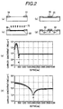
A manufacturing method of p-channel MOS transistor
using n-type silicone substrate is indicated in FIG. 2
as an example of conventional processes. First, in
accordance with publicly well known manufacturing process
of the MOS transistor as indicated in FIG. 2 (a), LOCOS
oxide film 10, 11 are formed on the n-type silicone
substrate. Then, as indicated in FIG. 2 (b), thermal
oxide film 80 is formed thinly, and p-type impurity layer
90 is formed by implanting p-type impurity ions (B+, or
BF2+, and the like) 70 into whole surface of the silicone
substrate by approximately 1012 - 1014 cm-2 with 10 - tens
keV. Then, as indicated in FIG. 2 (c), after removing
all the thermal oxide film 80 formed in FIG. 2(b), gate
oxide film 20 and gate electrode 30 are formed by the
publicly well known manufacturing process of the MOS
transistor, and p-channel MOS transistor indicated in FIG.
2 (d) can be obtained by forming source/drain regions by
the ion implantation method. FIG. 2(e) is a graph
indicating a concentration distribution of boron ions in
a depth direction under the gate oxide film 80, when the
boron ions are implanted with a dose of 1 x 1012 cm-2 by
an acceleration energy of 60 keV.
On the other hand, when high withstand voltage
elements having a withstand voltage of approximately 80V
or more and low withstand voltage MOS transistors having
a withstand voltage of such as 5V, 3.3V, 2.5V, and the
like are mounted on a chip concurrently, deep junction
is required for the impurity layer for forming channel
of the high withstand voltage element, and exact location
is required for diffusion region. Therefore, after
forming the gate oxide film and the gate electrode, the
location of the impurity layer is determined in a
self-adjusting method relating to the gate electrode, and
a heat treatment is performed for a long time. At that
time, if the shallow p-type impurity layer for
controlling a threshold voltage of the low withstand
voltage MOS transistor is formed before forming the gate
oxide film and gate electrode as in a conventional manner,
the shallow p-type impurity layer is diffused by a high
temperature treatment for the high withstand voltage
element. FIG. 2 (f) is a graph indicating a concentration
distribution of boron ions in a depth direction under the
gate oxide film 20 as an example, when the boron ions are
implanted with a dose of 1 x 1012 cm-2 by an acceleration
energy of 60 keV before forming the gate oxide film and
the gate electrode , and subsequently, a heat treatment
at 1100°C for 360 minutes is performed for forming the
channel layer of the high withstand voltage element. In
comparison with the FIG. 2 (e), it is revealed that the
surface concentration, which determined the threshold
voltage of the MOS transistor, is decreased. As the
result, the threshold voltage of the MOS transistor can
not be controlled. However, if the implantation dose is
increased in order to increase the surface concentration,
the junction depth of the p-type diffusion layer becomes
deep, and the p-type diffusion layers of the source region
and the drain region are combined, and the MOS transistor
becomes inoperable. Therefore, the presence of the high
withstand voltage element and the low withstand voltage
p-channel MOS transistor concurrently on a chip becomes
possible by utilizing prior art such as the manufacturing
method disclosed in JP-A-2-10841 (1990), wherein p-type
impurities are introduced so as to penetrate the gate
electrode and the gate oxide film after forming the gate
electrode.
In accordance with the above prior art, the size of
the element of low withstand voltage p-channel MOS
transistor is made small so as to realize high
integration; that is, if the length of the gate is
shortened, depletion layers of source junction and drain
junction are contacted; a phenomenon called as punch-through,
which means that the current becomes
uncontrollable by the gate; and a problem that the p-channel
MOS transistor becomes inoperable is generated.
SUMMARY OF THE INVENTION
The present invention is achieved in consideration of
the above problem of the prior art described above, and
aimed at providing a structure and a manufacturing method
of insulated gate transistor suitable for integrating
high withstand voltage elements and low withstand voltage
insulated gate transistors on a chip simultaneously.
The insulated gate transistor in accordance with the
present invention comprises; second conductive type
source region and drain region provided on surface of a
substrate of first conductive type semiconductor; and
gate electrodes provided on surface of the substrate of
the semiconductor via an insulating film at a region
located between the source region and the drain region.
Furthermore, the second conductive type semiconductor
layers having an impurity concentration lower than that
of the source region and the drain region are formed on
the surface of the substrate of the semiconductor at the
location beneath the gate electrode, and at a region
connected with the source region and the drain region and
deeper than the source region and the drain region in the
substrate of the semiconductor. An interval between the
deepest point at the portion connected with the source
region and the deepest point at the portion connected
with the drain region is set so as to be larger than the
gate length of the gate electrode. Here, the first
conductive type and the second conductive type are any
of p-type and n-type contrary each other.
In accordance with the present invention, the
depletion layers in the semiconductor substrate are
scarcely contacted each other at the region formed deeper
than the source region and the drain region in the second
semiconductor layer, because the interval between the
deepest point at the portion connected with the source
region and the deepest point at the portion connected with
the drain region is set so as to be larger than the gate
length of the gate electrode. Therefore, deterioration
of characteristics and impossibility of operation of the
semiconductor accompanied with contact of the depletion
layers can be prevented. The advantages of the present
invention are significant when the channels are shortened
by decreasing the gate length, and deterioration
accompanied with shortening the channels can be
prevented.
The insulated gate transistor described above is
manufactured by the following method. The manufacturing
method in accordance with the present invention comprises
the steps of the first process for forming the gate oxide
film and the gate electrode on the surface of the
semiconductor substrate, the second process for applying
resist or providing insulating member on side wall of the
gate electrode, and the third process for implanting ions
of the second conductive type impurity in the
semiconductor substrate using the gate oxide film, the
gate electrode, and the resist or the insulating member
as masks so that the impurity is introduced into the
surface of the semiconductor substrate located beneath
the gate electrode. The second conductive type impurity
is introduced deepest into the regions of the
semiconductor substrate, where are not masked with the
gate electrode, at both sides of the gate electrode,
respectively, but the depth of the introduction of the
second conductive type impurity in the region of the
semiconductor substrate coated with the resist or the
insulating member at the side wall of the gate electrode
is depressed. Therefore, subsequent to the third process
for forming the second conductive type source region and
the drain region, the interval between the deepest point
of the second conductive type semiconductor layer formed
in the second process in the region contacting with the
source region and the deepest point in the region
contacting with the drain region becomes longer than the
length of the gate of the source electrode.
The present invention relates to a semiconductor
integrated circuit device comprising fine insulated gate
transistor having small gate length, and its
manufacturing method is suitable for applying to the
semiconductor integrated circuit device including a high
temperature thermal treatment such as a case when high
withstand voltage semiconductor elements exist
simultaneously. That is, in a case when high energy ions
for adjusting a threshold voltage are implanted using the
gate electrode as a mask after the heat treatment by
proving the insulated member at the side wall of the gate
electrode, deterioration in the characteristics of the
insulated gate transistor; accompanied with contact of
the depletion layers between the layers of the
semiconductors formed deeply in the regions of the
semiconductor substrate, where are not masked with the
gate electrode, at both sides of the gate electrode; can
be prevented. The advantages of the present invention
are significant on the semiconductor integrated circuit
device comprising the insulated gate transistor having
short gate length and the semiconductor elements having
a high withstand voltage, and deterioration of the
characteristics of the fine insulated gate transistor can
be prevented.
BRIEF DESCRIPTION OF THE DRAWINGS
FIG. 1 is a schematic cross sectional view of p-channel
MOS transistor of the embodiment of the present invention,
FIG. 2 is a set of drawings indicating a conventional
manufacturing method of low withstand voltage p-channel
field effect transistor, and graphs indicating
concentration distribution of p-type impurity in the
channel region,
FIG. 3 is a set of graphs indicating the concentration
distribution of boron ions in the source/drain regions,
FIG. 4 is a set of graphs indicating a relationship
between the effective channel length of the MOS transistor,
and a relationship between the effective channel length
and ratio of the junction depth,
FIG. 5 is a set of drawings indicating the
manufacturing method of the p-channel MOS transistor of
the second embodiment of the present invention,
FIG. 6 is a set of drawings indicating the
manufacturing method of the p-channel MOS transistor of
the third embodiment of the present invention,
FIG. 7 is a set of drawings indicating the
manufacturing method of the p-channel MOS transistor of
the fourth embodiment of the present invention,
FIG. 8 is a set of drawings indicating the
manufacturing method of the p-channel MOS transistor of
the fifth embodiment of the present invention, and
FIG. 9 is a set of drawings indicating the
manufacturing method of the p-channel MOS transistor of
the sixth embodiment of the present invention.
DETAILED DESCRIPTION OF THE PREFERRED EMBODIMENTS
(Embodiment 1)
FIG. 1 is a schematic cross sectional view of p-channel
MOS transistor of the embodiment of the present invention.
LOCOS oxide films 10, 11 for separating elements are
formed on the surface of the n-type semiconductor
substrate, and p-type source 60 and drain 61 having a high
impurity concentration are formed on the surface of the
semiconductor substrate between these LOCOS oxide films.
Each of source electrode and drain electrode (not shown
in the figure) is connected by ohmic junction to the source
60 and the drain 61, respectively. MOS gate is formed
by providing thin gate silicone oxide film 20 and
polysilicon gate electrode 30 laminated thereon onto the
surface of the semiconductor substrate to be channel
region between the source 60 and the drain 61. The p-type
semiconductor layer for adjusting threshold voltage of
the MOS gate having a lower impurity concentration than
those of the source and the drain is formed in the region
from the surface of the semiconductor substrate just
beneath the gate electrode 30 to the region contacting
with the source 60 and the drain 61 in the semiconductor
substrate and deeper region than these semiconductor
regions. Only the portion on the surface of the
semiconductor substrate just beneath the gate electrode
30 of the p-type semiconductor layer 50 has substantially
a function to adjust the threshold voltage. However, in
accordance with forming the p-type semiconductor layer
50 to the region where the source 60 and the drain 61 are
located, the threshold voltage adjustment by the ion
implantation using the gate electrode as a mask becomes
possible as stated later. In the present embodiment, the
interval between the region contacting with the source
60 and the region contacting with the drain in the p-type
semiconductor layer 50, that is, the distance between
source and drain as indicated as LSD in the figure is
broadened as it goes deeper from the surface of the
semiconductor substrate, and the interval Ld at the
deepest point becomes larger than the width of the gate
electrode 30, that is, the gate length LG. Therefore,
generation of punch-through of the depletion layers
between the source and the drain becomes difficult, and
operation of the p-channel MOS transistor becomes
sufficiently possible, even if the gate length is as
shortened as equal to or less than 2 µm.
In order to broaden the LSD as it goes deeper from the
surface of the semiconductor substrate, insulating films
40, 41 made of silicon oxide are provided at the side wall
of the gate electrode 30. the silicon oxide is formed
being adhered to the side wall of the gate electrode 30
extending along the side wall to the portion off the end
of the gate electrode of the gate oxide film 20. In
accordance with the composition of the element having the
insulating films 40, 41, the p-type semiconductor layer
50 such as the present embodiment can be formed by ion
implantation using the gate electrode 30 as a mask as
stated later.
In accordance with the present embodiment, adjustment
of the threshold voltage by ion implantation using the
gate electrode as the mask becomes possible, and channel
shortening becomes possible even if the p-type
semiconductor layer 50 has a portion deeper than the
source 60 and the drain 61. Accordingly, in accordance
with the present embodiment, the p-channel MOS transistor
having short channel and the semiconductor element having
a high withstand voltage (for instance, IGBT) can be
integrated on a same semiconductor chip as explained later
in the embodiment.
The conditions for the composition of the present
embodiment operating certainly as the p-channel MOS
transistor studied by the inventors of the present
invention are explained hereinafter.
A result of simulation study on variation of the
threshold value is indicated in FIG. 4(a); when effective
channel length (a distance between the source and the
drain LCD under the gate oxide film, that is, the width
of the p-type semiconductor layer 50 under the gate oxide
film in a direction of the gate length) is varied using
the ratio of the p-channel MOS transistor having a
junction depth xj1 of the p-type semiconductor layer 50
contacting with the source and drain in the range of
approximately 3000-6000 Å to the junction depth xj2 of the
p-type semiconductor layer 50 under the gate oxide film
as a parameter. When the ratio of the junction depth (xj2
/xj1) of the p-type semiconductor layer 50 becomes larger
than 0.25, the composition does not operate as the MOS
transistor, nor the threshold voltage can be determined.
When the ratio is smaller than 0.05, the threshold voltage
can not be controlled. Generally, the MOS transistor is
designed so that the threshold voltage varies in the range
of ±0.15 V, in order to depress the variation of the
threshold voltage depending on the temperature change,
and variation in drain current depending on the elevation
of the threshold voltage. Therefore, in accordance with
the FIG. 4 (a), the critical effective channel length off
the range of ±0.15 V is determined, and a relationship
between the ratio of junction depth of the p-type
semiconductor layer 50 and the critical effective channel
length off the range of ±0.15 V is determined. The
result is indicated in FIG. 4 (b). The p-channel MOS
transistor operates certainly, if the ratio of the
junction depth and the effective channel length of the
transistor are in the region of the hatched area of the
FIG. 4(b).
(Embodiment 2)
FIG. 5 is a set of the schematic cross sections of the
p-channel MOS transistor indicating the steps of the
manufacturing method of the second embodiment of the
present invention.
As indicated in FIG. 5 (a), LOCOS oxide film 10, 11
are formed on a n-type silicon substrate by a conventional
MOS transistor manufacturing method, and a region wherein
the MOS transistor is formed is made an active region.
Then, as indicated in FIG. 5 (b), gate silicon oxide film
20 is accumulated in a height of tens-hundreds Å by thermal
growth method, and n-type polysilicon film 30 is
accumulated in a height of hundreds-thousands Å by CVD
method. Subsequently, a photoprocess is performed on the
gate silicon oxide film 20 and the polysilicon film 30
so as to remain a gate region of gate length 0.5 µm -
2 µm, and unnecessary region is removed by dry etching.
Then, as indicated in FIG. 5(c), resist 100 is applied
onto the portion other than the polysilicon with the
thickness of at least 2 µm so as to be adhered to the
side wall of the silicon film in the gate region, and ion
implantation is performed on the whole surface of the
silicon substrate with p-type impurity ions (B+ or BF2+,
and the like) 70 by tens-hundreds keV. After removing
the resist applied in the process of FIG. 5 (c), the resist
of thousands Å thick is applied onto the upper plane of
the polysilicon and a width of hundreds nm to a several
microns from the side plane of the polysilicon as
indicated in FIG. 5 (d). Here, ion implantation is
performed on the whole surface of the silicon substrate
with p-type impurity ions (B+ or BF2+, and the like) 70
by tens-hundreds keV. Subsequently, the source/ drain
regions 60, 61 of the p-channel MOS transistor are formed
by the conventional MOS transistor manufacturing process
as indicated in FIG. 5 (e).
In accordance with the ion implantation performed in
the process indicated in FIG. 5 (d), the punch-through
is suppressed, because the end portion of the source/drain
does not reach the beneath portion of the side wall of
the gate electrode. Shallow p-type impurity layer 51 is
formed exactly beneath the gate electrode by the process
indicated in FIG. 5(c), and the threshold voltage of the
manufactured p-channel MOS transistor can be controlled
to be a desired value.
The p-type impurity layers 50, 51, 52 for adjusting
the threshold voltage can not form ohmic contact with the
source and drain electrodes (not shown in the figure),
because the impurity concentration is low. Therefore,
p-type impurity is further implanted to be a concentration
capable of forming the ohmic contact (generally, at least
1 X 10¹⁵ /cm2) to form the source 60 and the drain 61.
Generally, when the fine p-channel MOS transistor is
manufactured, the depths of the p-type source and the
drain must be shallow as the gate length becomes shorter
in order to prevent the contact of the depletion layers.
Then, generally, in the process of the gate length of 1.3
µm for instance, the source and the drain are formed by
the ion implantation using B+ with 30 keV, and BF2+ with
60 keV. If the gate length is shortened, the same or lower
acceleration energy as the above acceleration energy is
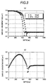
used. FIG. 3 (a) indicates a concentration distribution
of boron ions in a depth direction in a case when the ion
implantation is performed with B+ with the acceleration
energy of 30 keV, and BF2+ with the acceleration energy
of 60 keV, and subsequent conventional processes for
recoverying defects and forming interlayer insulating
film are performed. When the MOS transistor having the
gate length of 1.3 µm is manufactured, the junction depth
of the source/drain of a high concentration becomes
approximately 450-500 nm.
On the other hand, in order to form the p-type impurity
layer 51 just beneath the gate oxide film, the ions must
be implanted by the acceleration energy with the surface
concentration sufficiently exceeding 1 X 10¹⁶/cm3 for
penetrating the gate electrode and the gate oxide film,
and adjusting the threshold voltage of the p-channel MOS
transistor. The thickness of the gate electrode is
approximately 3000-4000 Å for n-type polysilicon in the
process of conventional gate length of approximately 1
µm, approximately 1000 Å for n-type polysilicon and
approximately 1500 Å for polycide or silicide and the like
in the process of gate length of approximately 0.8 µm.
Because an indispensable condition for the gate electrode
is low resistance, even if the gate length is shortened,
significant change in the thickness is not necessary.
Thickness of the gate oxide film is approximately 100-300
Å. In a case when the gate oxide film of 250 Å and
polysilicon film of 3500 Å are used, which are generally
used in the process for gate length of approximately 1.3
µm, an acceleration energy equal to or more than 100 keV
is necessary for implanting B+ through the gate oxide film
and exceeding the surface concentration of 1 X 10¹⁶ /cm3
sufficiently. In another case when the gate oxide film
of 180 Å, and polysilicon film of 1000 Å and silicide
of 1500 Å as the gate electrode are used, which are
generally used in the process for gate length of
approximately 0.8 µm, an acceleration energy equal to or
more than 80 keV is necessary for implanting B+. Even
if the gate length is shortened, the thickness is not
changed significantly, because low resistance is
indispensable. Therefore, in order to maintain the
surface concentration of exceeding 1 X 10¹⁶ /cm3
sufficiently, an acceleration energy equal to or more than
90 keV is necessary for implanting B+.
FIG. 3(b) is a graph indicating a concentration
distribution of B+ in a depth direction of the p-type
semiconductor layers 50, 52, which are formed
simultaneously with formation of the p-type semiconductor
layer 51 by implanting B+ by an acceleration energy of
90 keV. The figure reveals that the junction depth is
approximately 550 pm. As indicated in the figure, the
p-type semiconductor layers 50, 52 of relatively low
concentration exist in positions of the junction depth
deeper than the source 60 and the drain 61 of high
concentration. With the p-channel MOS transistor having
the gate length of equal to or less than 1.3 µm, ensuring
a distance between the source and the drain equal to or
more than the gate length is necessary at the junction
depth position of the low concentration in order to
prevent contact of the depletion layers.
In accordance with the present embodiment, ion
implantation is performed with applying resist 100 onto
the side wall of the gate 30. Therefore, the interval
between the p-type semiconductor layers 50, 52, that is
the source·drain interval Ld at the deepest point shown
in FIG. 1, can be made longer than the gate length.
In accordance with the present embodiment, an example
of only n-type silicon substrate is indicated. However,
the present invention is applicable to any of p-type
silicon substrate, SOI substrate, DI separated substrate,
and other.
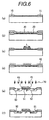
(Embodiment 3)
FIG. 6 is a set of the schematic cross sections of the
p-channel MOS transistor indicating the steps of the
manufacturing method of the third embodiment of the
present invention.
As indicated in FIG. 6 (a), LOCOS oxide film 10, 11
are formed on a n-type silicon substrate by a conventional
MOS transistor manufacturing method, and a region wherein
the MOS transistor is formed is made an active region.
Then, as indicated in FIG. 6 (b), gate silicon oxide film
20 is accumulated in a height of tens-hundreds Å by thermal
growth method, and n-type polysilicon film 30 is
accumulated in a height of hundreds-thousands Å by CVD
method. Subsequently, a photoprocess is performed on the
gate silicon oxide film 20 and the polysilicon film 30
so as to remain a gate region of gate length 0.5 µm -
2 µm as indicated in FIG. 6(c), and unnecessary region
is removed by dry etching. Then, silicon oxide film 42
is accumulated on all the surface of the silicon substrate
in a height of thousands Å by CVD method. By performing
an anisotropic etching on the accumulated silicon oxide
film by dry etching method, the side walls 40, 41 of the
silicon oxide film, an insulating material, are remained;
the silicon oxide film is adhered to the side planes along
the polysilicon film in the gate region until reaching
the gate oxide film as indicated in FIG. 6(e). Here, ion
implantation is performed on the whole surface of the
silicon substrate with p-type impurity ions (B+ or BF2+,
and the like) 70 by tens-hundreds keV. Subsequently, the
source/ drain regions 60, 61 of the p-channel MOS
transistor are formed by the conventional MOS transistor
manufacturing process, and the p-channel MOS transistor
as indicated in FIG. 6 (f) is obtained.
In accordance with performing the ion implantation of
p-type impurity ions through the gate electrode and the
gate oxide film, a shallow p-type impurity layer 51 is
formed exactly beneath the gate electrode, and the
threshold voltage of the manufactured p-channel MOS
transistor can be controlled to be a desired value.
In accordance with the present embodiment, an example
of only n-type silicon substrate is indicated. However,
the present invention is applicable to any of p-type
silicon substrate, SOI substrate, DI separated substrate,
and other.
(Embodiment 4)
FIG. 7 is a set of the schematic cross sections of
semiconductor integrated circuit device, wherein
enhancement type n-channel MOS transistors and p-channel
MOS transistors are formed on a chip, indicating
the steps of the manufacturing method of the fourth
embodiment of the present invention.
As indicated in FIG. 7 (a), LOCOS oxide film 10, 11,
12 are formed on a n-type silicon substrate by a
conventional MOS transistor manufacturing method, and
regions wherein the p-channel and the n-channel MOS
transistors are formed are made active regions. In the
region, whereon the n-channel MOS transistor is formed,
p-well 200 is formed by ion implantation of p-type
impurity such as boron ions and the like and heat treatment
at a high temperature. Then, as indicated in FIG. 7 (b),
gate silicon oxide film 20 is accumulated in a height of
tens-hundreds Å by thermal growth method, and n-type
polysilicon film 30 is accumulated in a height of
hundreds-thousands Å by CVD method. Subsequently, a
photoprocess is performed on the gate silicon oxide film
20 and the polysilicon film 30 so as to remain a gate region
of gate length 0.5 µm - 2 µm in each of the regions,
wherein the n-channel MOS transistor and the p-channel
MOS transistor are formed respectively as indicated in
FIG. 7(c), and unnecessary region is removed by dry
etching. Then, silicon oxide film 44 is accumulated on
all the surface of the silicon substrate in a height of
thousands Å by CVD method. By performing an anisotropic
etching on the accumulated silicon oxide film by dry
etching method, the side walls 40, 41, 42, 43 of the silicon
oxide film are remained at side planes of the gate silicon
oxide film and the polysilicon film. Here, ion
implantation is performed on the whole surface of the
silicon substrate with p-type impurity ions (B+ or BF2+,
and the like) 70 by tens-hundreds keV. Subsequently,
p-type source/ drain regions 62, 63 are formed in the
region forming the p-channel MOS transistor and n-type
source/ drain regions 60, 61 are formed in the region
forming the n-channel MOS transistor by the conventional
MOS transistor manufacturing process.
In accordance with performing the ion implantation of
p-type impurity ions through the gate electrode, shallow
p-type impurity layers 50, 51 are formed exactly beneath
the gate electrode, and the threshold voltages of both
the manufactured p-channel MOS transistor and n-channel
MOS transistor can be controlled to be desired values.
In accordance with the present embodiment, an example
of only n-type silicon substrate is indicated. However,
the present invention is applicable to any of p-type
silicon substrate, SOI substrate, DI separated substrate,
and other.
(Embodiment 5)
FIG. 8 is a set of the schematic cross sections of
semiconductor integrated circuit device, wherein high
withstand voltage n-channel MOS transistors and low
withstand voltage p-channel MOS transistors are formed
on a chip, indicating the steps of the manufacturing
method of the fifth embodiment of the present invention.
As indicated in FIG. 8 (a), LOCOS oxide film 10, 11,
12, 13 are formed on a n-type silicon substrate by a
conventional MOS transistor manufacturing method, and
regions wherein the high withstand voltage n-channel MOS
transistors and low withstand voltage p-channel MOS
transistors are formed are made active regions. An n-well
is formed by ion implantation of n-type impurity 90
such as phosphorus and the like and heat treatment at a
high temperature. Then, as indicated in FIG. 8 (b), gate
silicon oxide film 20 is accumulated in a height of
tens-hundreds Å by thermal growth method, and n-type
polysilicon film 30 is accumulated in a height of
hundreds-thousands Å by CVD method. Subsequently, a
photoprocess is performed on the gate silicon oxide film
20 and the polysilicon film 30 so as to remain gate regions
of gate length L2, L3 of several µm for the high withstand
voltage n-channel field effect transistor and the gate
regions of gate length L1 of 0.5 - 2 µm for the low
withstand voltage p-channel field effect transistor,
respectively as indicated in FIG. 8(c), and unnecessary
region is removed by dry etching. Then, p-type impurity
ions (B+ or BF2+ and others) 70 are introduced into only
the region of the high withstand voltage n-channel MOS
transistor by ion implantation, and deep p-type impurity
layer 65 as indicated in FIG. 8 (d) is formed by thermal
diffusion process at hundreds to a thousand and several
hundreds degrees for tens - several hundreds minutes.
Then, silicon oxide film 44 is accumulated on all the
surface of the silicon substrate in a height of thousands
Å by CVD method. By performing an etching on the
accumulated silicon oxide film by dry etching method, the
side walls 40, 41, of the silicon oxide film are remained
at side planes of the gate silicon oxide film and the
polysilicon film as indicated in FIG. 8 (e). Here, ion
implantation is performed on only the region of the low
withstand voltage p-channel field effect transistor with
p-type impurity ions (B+ or BF2+, and the like) 70 by
tens-hundreds keV to form the p-type impurity layer 50.
Subsequently, n-type source/ drain regions 62, 63 are
formed in the region forming the high withstand voltage
n-channel MOS transistor and p-type source/ drain regions
60, 61 are formed in the region forming the low withstand
voltage p-channel MOS transistor by the conventional MOS
transistor manufacturing process.
In accordance with the low withstand voltage p-channel
MOS transistor manufactured as above, the ion
implantation of p-type impurity ions for adjusting the
threshold voltage is performed after completion of the
gate electrode. Accordingly, the low withstand voltage
p-channel MOS transistor is not influenced by the heat
treatment at a high temperature for forming channel stop
region of the high withstand voltage n-channel MOS
transistor, and the threshold value of the p-channel MOS
transistor can be controlled to be a desired value.
In accordance with the present embodiment, an example
of only n-type silicon substrate is indicated. However,
the present invention is applicable to any of p-type
silicon substrate, SOI substrate, DI separated substrate,
and other. Furthermore, an embodiment of forming the high
withstand voltage n-channel MOS transistor and the low
withstand voltage p-channel MOS transistor on a chip is
indicated, but high withstand voltage p-channel MOS
transistor and the low withstand voltage p-channel MOS
transistor can be formed similarly on a chip.
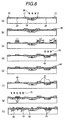
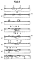
(Embodiment 6)
FIG. 9 is a set of the schematic cross sections of
semiconductor integrated circuit device, wherein IGBT and
p-channel MOS transistors are formed on a chip, indicating
the steps of the manufacturing method of the sixth
embodiment of the present invention.
As indicated in FIG. 9 (a), LOCOS oxide film 10, 11,
12, 13 are formed on a n-type silicon substrate by a
conventional MOS transistor manufacturing method, and
regions wherein the field effect transistors and the IGBT
are formed are made active regions. Then, as indicated
in FIG. 9 (b), gate silicon oxide film 20 is accumulated
in a height of tens-hundreds Å by thermal growth method,
and n-type polysilicon film 30 is accumulated in a height
of hundreds-thousands Å by CVD method. Subsequently, a
photoprocess is performed on the gate silicon oxide film
20 and the polysilicon film 30 so as to remain gate regions
of gate length L of several µm for the IGBT and the gate
regions of gate length L of 0.5 - 2 µm for the low withstand
voltage p-channel MOS transistor, respectively as
indicated in FIG. 9(c), and unnecessary region is removed
by dry etching. Then, p-type impurity ions 90 are
introduced into only the region of the IGBT by ion
implantation and by thermal diffusion process at hundreds
to a thousand and several hundreds degrees for tens -
several hundreds minutes for forming the deep p-type
impurity layer 61 as indicated in FIG. 9 (d).
Subsequently, p-type impurity ions are introduced
similarly by ion implantation and thermal diffusion
process at hundreds to a thousand and several hundreds
degrees for tens - several hundreds minutes for forming
the p-type impurity layer 60. Furthermore, ion
implantation is performed for forming n-type anode of the
IGBT. Then, silicon oxide film 44 is accumulated on all
the surface of the silicon substrate in a height of
thousands Å by CVD method as indicated in FIG. 9 (e). By
performing an etching on the accumulated silicon oxide
film by dry etching method, the side walls 40, 41, 423,
43 of the silicon oxide film are remained at side planes
of the gate silicon oxide film and the polysilicon film
as indicated in FIG. 9 (f). Here, ion implantation is
performed on only the region of the low withstand voltage
p-channel field effect transistor with p-type impurity
ions (B+ or BF2+, and the like) 70 by tens-hundreds keV
to form the p-type impurity layer 50. Subsequently,
p-type collector 65 is formed for the IGBT, and p-type
source/ drain regions 63, 64 are formed for the low
withstand voltage p-channel MOS transistor by the
conventional IGBT and MOS manufacturing process.
In accordance with the low withstand voltage p-channel
MOS transistor manufactured as above, the ion
implantation of p-type impurity ions for adjusting the
threshold voltage is performed after completion of the
gate electrode. Accordingly, the low withstand voltage
p-channel MOS transistor is not influenced by the heat
treatment at a high temperature for forming channel stop
region of the IGBT, and the threshold value of the p-channel
MOS transistor can be controlled to be a desired
value.
As explained above, the IGBT and the low withstand
voltage p-channel MOS transistor can be mounted on a same
chip.
In accordance with the present embodiment, an example
of only n-type silicon substrate is indicated. However,
the present invention is applicable to any of p-type
silicon substrate, SOI substrate, DI separated substrate,
and other.
As explained above, in accordance with the present
invention, the high withstand voltage elements and short
channel fine low withstand voltage MOS transistor can be
existed simultaneously.