EP0944014A2 - Transponder system and method - Google Patents
Transponder system and method Download PDFInfo
- Publication number
- EP0944014A2 EP0944014A2 EP99301824A EP99301824A EP0944014A2 EP 0944014 A2 EP0944014 A2 EP 0944014A2 EP 99301824 A EP99301824 A EP 99301824A EP 99301824 A EP99301824 A EP 99301824A EP 0944014 A2 EP0944014 A2 EP 0944014A2
- Authority
- EP
- European Patent Office
- Prior art keywords
- excitation signal
- rfid device
- circuit
- signal generator
- generator circuit
- Prior art date
- Legal status (The legal status is an assumption and is not a legal conclusion. Google has not performed a legal analysis and makes no representation as to the accuracy of the status listed.)
- Granted
Links
Images


Classifications
-
- G—PHYSICS
- G06—COMPUTING OR CALCULATING; COUNTING
- G06K—GRAPHICAL DATA READING; PRESENTATION OF DATA; RECORD CARRIERS; HANDLING RECORD CARRIERS
- G06K7/00—Methods or arrangements for sensing record carriers, e.g. for reading patterns
- G06K7/10—Methods or arrangements for sensing record carriers, e.g. for reading patterns by electromagnetic radiation, e.g. optical sensing; by corpuscular radiation
- G06K7/10009—Methods or arrangements for sensing record carriers, e.g. for reading patterns by electromagnetic radiation, e.g. optical sensing; by corpuscular radiation sensing by radiation using wavelengths larger than 0.1 mm, e.g. radio-waves or microwaves
- G06K7/10118—Methods or arrangements for sensing record carriers, e.g. for reading patterns by electromagnetic radiation, e.g. optical sensing; by corpuscular radiation sensing by radiation using wavelengths larger than 0.1 mm, e.g. radio-waves or microwaves the sensing being preceded by at least one preliminary step
- G06K7/10128—Methods or arrangements for sensing record carriers, e.g. for reading patterns by electromagnetic radiation, e.g. optical sensing; by corpuscular radiation sensing by radiation using wavelengths larger than 0.1 mm, e.g. radio-waves or microwaves the sensing being preceded by at least one preliminary step the step consisting of detection of the presence of one or more record carriers in the vicinity of the interrogation device
-
- G—PHYSICS
- G06—COMPUTING OR CALCULATING; COUNTING
- G06K—GRAPHICAL DATA READING; PRESENTATION OF DATA; RECORD CARRIERS; HANDLING RECORD CARRIERS
- G06K19/00—Record carriers for use with machines and with at least a part designed to carry digital markings
- G06K19/06—Record carriers for use with machines and with at least a part designed to carry digital markings characterised by the kind of the digital marking, e.g. shape, nature, code
- G06K19/067—Record carriers with conductive marks, printed circuits or semiconductor circuit elements, e.g. credit or identity cards also with resonating or responding marks without active components
- G06K19/07—Record carriers with conductive marks, printed circuits or semiconductor circuit elements, e.g. credit or identity cards also with resonating or responding marks without active components with integrated circuit chips
- G06K19/0723—Record carriers with conductive marks, printed circuits or semiconductor circuit elements, e.g. credit or identity cards also with resonating or responding marks without active components with integrated circuit chips the record carrier comprising an arrangement for non-contact communication, e.g. wireless communication circuits on transponder cards, non-contact smart cards or RFIDs
-
- G—PHYSICS
- G06—COMPUTING OR CALCULATING; COUNTING
- G06K—GRAPHICAL DATA READING; PRESENTATION OF DATA; RECORD CARRIERS; HANDLING RECORD CARRIERS
- G06K7/00—Methods or arrangements for sensing record carriers, e.g. for reading patterns
- G06K7/0008—General problems related to the reading of electronic memory record carriers, independent of its reading method, e.g. power transfer
Definitions
- the present invention relates to an RF transponder system and to a method of detecting an RF identification device.
- Embodiments of the present invention relate to operation of a radio frequency transponder system having a radio frequency reader unit and a radio frequency identification device and, to a method of operating the radio frequency transponder system to detect the proximity of the radio frequency identification device to the radio frequency reader unit which is in a reduced power state.
- a radio frequency (RF) transponder system typically comprises an RF reader unit and a radio frequency identification (RFID) device.
- the RFID device is commonly termed an RFID tag. Operation of the RF transponder system is generally characterised by multiple operating modes including excitations, response and read modes. The RF transponder system requires electrical power to operate in each of these modes. In particular, the RF reader unit must be powered during the excitation and read modes while the RFID device must be powered during the response mode. In many conventional RF transponder systems the RFID device is a passive device, i.e., the RFID device lacks an internal power source or physical connection to an external power source. The passive RFID device is powered remotely by the RF reader unit while the RFID device is free of contact with the RF reader unit. An example of a passive RFID device and its method of operation are disclosed in US Patent 4,730,188 to Milheiser. The RF reader unit is conventionally connected to an electrical power source, such as an ac power line, which powers the RF reader unit.
- an electrical power source
- An embodiment of the present invention seeks to provide an RF reader unit, which is powered by a self-contained portable power source integral with the RF reader unit, such as a small disposable or rechargeable battery.
- a self-contained portable power source integral with the RF reader unit, such as a small disposable or rechargeable battery.
- This enables the user to position the RF reader unit in a remote location which lacks access to an ac power line or an ac power outlet.
- a battery however, has a finite life necessitating replacement of the battery in the RF reader unit at the end of its useful life, which is both costly and time consuming. Accordingly, it is desirable to reduce the power demands on the battery of the RF reader unit during operation of the RF transponder system, thereby extending the useful life of the battery.
- an embodiment of the present invention seeks to provide an RF transponder system operable at a reduced electrical power state.
- An embodiment of the present invention seeks to provide a method of operating an RF transponder system in a power conserving manner, wherein the system transitions between a reduced power state and an increased power state as a function of the specific operating mode of the system.
- An embodiment of the present invention seeks to provide such a method, wherein the RF transponder system has an effective RFID device detection mode of operation at a reduced power state and has excitation, response and read modes of operation at an increased power state.
- Another embodiment of the present method seeks to provide such a method, wherein the power requirements of the RF transponder system are fully satisfied by a disposable or rechargeable battery residing in the RF reader unit of the system.
- An embodiment of the present invention provides a method of operating an RF transponder system comprising an RF reader unit and a passive RFID device.
- the RF reader unit includes an excitation signal generator circuit, an excitation mode activation circuit coupled to the excitation signal generator circuit, an RFID device detection circuit coupled to the excitation mode activation circuit, and a power source for powering the electrical components of the RF reader unit.
- the excitation signal generator circuit is operable in either a reduced power state or an increased power state. When operating in the reduced power state, the excitation signal generator circuit enables generation of a plurality of ring signals which exhibit an RFID device detection parameter. When operating in the increased power state, the excitation signal generator circuit enables generation of an RF excitation signal which powers the RFID device.
- the excitation mode activation circuit which is preferably a logic flip/flop switch, enables switching of the excitation signal generator circuit between the reduced power state and the increased power state in response to the RFID device detection parameter passing a variation threshold level.
- the RFID device detection circuit is operable in the reduced power state to determine when the RFID device detection parameter passes the variation threshold level.
- the power source is in the form of a small portable battery which provides reduced electrical current to the excitation signal generator circuit in the reduced power state and increased electrical current to the excitation signal generator circuit in the increased power state.
- the RFID device includes a transponder circuit which causes the RFID device detection parameter of the ring signals to pass the variation threshold level when the RFID device is positioned in a proximal space relative to the RF reader unit.
- An embodiment of the present invention provides a method of operating the RF transponder system to detect the presence of the RFID device in the proximal space of the RF reader unit.
- the method is initiated with the excitation signal generator circuit of the RF reader unit operating in a reduced power state which is effected by drawing reduced electrical current from the power source.
- the excitation signal generator circuit generates the ring signals in response to the reduced electrical current and transmits the ring signals into the proximal space.
- the RFID device detection circuit of the RF reader unit which is in electrical communication with the excitation signal generator circuit, receives and evaluates the ring signals to determine variations in the RFID device detection parameter of the ring signals, such as variations in the decay rate or average voltage of the ring signals.
- the excitation mode activation circuit transitions the excitation signal generator circuit from the reduced power state to the increased power state and generation of the ring signals is terminated.
- the excitation signal generator circuit draws increased electrical current from the power source in the increased power state to generate the RF excitation signal.
- the RF excitation signal is transmitted to the RFID device positioned in the proximal space, powering the transponder circuit of the RFID device.
- the ring signals and the RF excitation signal have substantially the same frequency which is substantially equal to the tuned frequency of the transponder circuit and the excitation signal generator circuit.
- the transponder circuit processes the RF excitation signal, generates an RF response signal in response to the RF excitation signal, and transmits the RF response signal to an ER circuit housed in the RF reader unit.
- the ER circuit which includes the excitation signal generator and RFID device detection circuits, reads the RF response signal upon receipt. After the RF response signal is read, the excitation signal generator circuit is transitioned back to the reduced power state and generation of the ring signals resumes while generation of the RF excitation signal is terminated.
- the duty cycle of the excitation signal generator circuit is substantially lower when operating in the reduced power state than when operating in the increased power state. As a result, the life of the power source is substantially extended and more electrical power is available to the other operations of the RF transponder system.
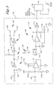
- the RF transponder system 10 comprises an RF reader unit 12 and a passive RFID device 14.
- the RF reader unit 12 includes an excitation signal generator circuit 16, an RFID device detection circuit 18, an excitation mode activation circuit 20, a response signal conditioner circuit 22, a response signal demodulation and detection circuit 24 and a power source 26.
- the power source 26 is typically a relatively small battery consisting of one or more disposable dry cells or rechargeable cells.
- the excitation signal generator circuit 16 includes a transmitter antenna coil 28 and the response signal conditioner circuit 22 includes a receiver antenna coil 30.
- An output device 32 such as a visual, audible or mechanical output, is coupled to the response signal demodulation and detection circuit 24.
- the circuits 16, 18, 20, 22, 24 of the RF reader unit 12 in combination are termed an exciter/reader (ER) circuit 34.
- ER exciter/reader
- Skilled artisans can appreciate that the RF reader unit 12 can be adapted to include a writer circuit (not shown) capable of writing programming instructions to the RFID device 14 by either contact or contactless means.
- the ER circuit 34 and writer circuit in combination are termed an exciter/reader/writer (ERW) circuit.
- Skilled artisans can further appreciate that the RF reader unit 12 can be adapted in accordance with the present invention to combine the functions of the transmitter antenna coil 28 and receiver antenna coil 30 in a single transmitter/receiver antenna coil.
- the passive RFID device 14 includes a transponder circuit 36 mounted on a support 38 such as a card.
- a passive RFID device having a transponder circuit mounted on a support is commonly termed an RFID tag.
- the transponder circuit 36 is a conventional circuit such as described in U.S. Patent 4,730,188 to Milheiser, incorporated herein by reference.
- the transponder circuit 36 generally includes a transmitter/receiver antenna coil 40 and a capacitor 42 coupled to a coil interface 44.
- a controller 46 is coupled to the coil interface 44 and to a memory 48. Skilled artisans can appreciate that the RFID device 14 can be adapted in to separate the functions of the transmitter/receiver antenna coil 40 into separate transmitter and receiver antenna coils in the manner of the ER circuit 34.
- the RF transponder system 10 has multiple modes of operation, including a detection mode, an excitation mode, a response mode and a read mode.
- the detection mode is the initial operating mode, wherein the RFID device 14 has a substantially passive function and the RF reader unit 12 has a substantially active function.
- the RF reader unit 12 employs the RFID device detection circuit 18 in cooperation with the excitation signal generator circuit 16 to actively seek detection of the RFID device 14 in a space 49 away from, but proximal to, the RF reader unit 12.
- the system 10 transitions the RF reader unit 12 to the excitation mode, wherein the excitation mode activation circuit 20 signals the excitation signal generator circuit 16 to generate an RF excitation signal 50.
- the RF excitation signal 50 is transmitted by the transmitter antenna coil 28 of the RF reader unit 12 and received by the transmitter/receiver antenna coil 40 of the RFID device 14.
- the system 10 transitions the RFID device 14 to the response mode, wherein the RFID device 14 is activated.
- the transponder circuit 36 When the RFID device 14 is in the response mode, the transponder circuit 36 generates an RF response signal 52, typically containing data associated with the RFID device 14, which is of interest to a user of the RF transponder system 10.
- the RF response signal 52 is transmitted by the transmitter/receiver antenna coil 40 of the RFID device 14 and is received by the receiver antenna coil 30 of the RF reader unit 12.
- the system 10 then transitions the RF reader unit 12 to the read mode, wherein the RF response signal 52 is processed by the ER circuit 34 and the data contained in the RF response signal 52 is communicated to the output device 32.
- An example of a method in accordance with the invention for performing the detection mode of operation enables the RF reader unit 12 to automatically detect whether the RFID device 14 is in the proximal space 49 while the system 10 is substantially in a reduced power state. Upon detection of the RFID device 14 in the proximal space 49, the system 10 transitions to an increased power state for the remaining excitation, response and read modes of operation.
- the excitation signal generator circuit 16 employed in the practice of the present invention is shown in greater detail.
- the excitation signal generator circuit 16 comprises in sequence an oscillator 54, a first Schmitt trigger 56, a pulse shaping circuit 58, a second Schmitt trigger 60, an antenna coil driver circuit 62, the transmitter antenna coil 28, and a ring signal processing circuit 64.
- the oscillator 54 is an astable multivibrator including an amplifier 66, a pair of resistors 68a, 68b, and a capacitor 70.
- a diode 72 and a resistor pair 74a, 74b are positioned in the excitation signal generator circuit 16 ahead of the oscillator 54.
- the pulse shaping circuit 58 includes a capacitor 76, a clock 78, a diode 80 and a resistor 82.
- the antenna coil driver circuit 62 includes a plurality of inverters 84a, 84b, 84c, 84d, 84e, 84f positioned in parallel.
- the ring signal processing circuit 64 has an RC network which includes a first capacitor 86, a resistor 88 and a second capacitor 90 in series.
- the ring signal processing circuit 64 also has a diode 92.
- the RFID device detection circuit 18 of Figure 1 comprises a sample and hold circuit 94 and a timing circuit 96.
- the sample and hold circuit 94 comprises in sequence a capacitor 98, a pair of unbalanced biasing resistors 100a, 100b, a first operational amplifier 102, an analog switch 104, a storage capacitor 106, a second operational amplifier 108, a ring signal change circuit 110 and a CMOS Schmitt trigger 112.
- the ring signal change circuit 110 includes a pair of resistors 114a, 114b and a capacitor 116.
- the timing circuit 96 comprises a sample time delay generator 118, a positive sample length pulse generator 120 and a negative sample length pulse generator 122.
- the sample time delay generator 118 is a first Schmitt trigger 124 positioned after a resistor 126 and a capacitor 128.
- the positive sample length pulse generator 120 is a second Schmitt trigger 130 positioned after a resistor 132 and a capacitor 134.
- the negative sample length pulse generator 122 is a third Schmitt trigger 136.
- the preferred excitation mode activation circuit 20 is a logic flip/flop switch as shown.
- the RF transponder system 10 automatically initiates the detection mode of operation upon powering the system 10 and continuously maintains the detection mode of operation as long as no RFID device 14 is in the proximal space 49 of the RF reader unit 12.
- the detection mode is powered by drawing a reduced electrical current from the power source 26 to the oscillator 54.
- the reduced electrical current demand on the power source 26 during the detection mode of operation is generally in the range of about 10 to about 30 microamps.
- a preferred power source 26 is a battery of 4 AA cells constituting a stored energy value of 1 amp-hr with a potential of 6 V.
- a representative value of the total current drain from the power source 26 is 40 microamps at 6 V, which corresponds to an extended battery life of 1 year.
- the oscillator 54 produces the ring generating pulses at a selected ring generating pulse rate which is sufficiently high to enable rapid detection of a nearby RFID device 14 in the manner described herein.
- An example of a selected ring generating pulse rate is 50 Hz.
- the ring generating pulses pass through the first Schmitt trigger 56 where the ring generating pulses are formed into square waves designated 138, as shown in Figure 2 downstream of the first Schmitt trigger 56.
- the square-waved ring generating pulses 138 are routed through the pulse shaping circuit 58 and the antenna coil driver circuit 62, which optimize the shape of the ring generating pulses to a selected width.
- the second Schmitt trigger 60 is provided between the pulse shaping circuit 58 and the antenna coil driver circuit 62 as a buffer to maintain the shape of the ring generating pulses in the pulse shaping circuit 58.
- the optimized ring generating pulses 140 have an appearance as shown in Figure 2 downstream of the antenna coil driver circuit 62.
- the optimal pulse width of the shaped ring generating pulse 140 is preferably selected as a function of the frequency to which the LC networks of the excitation signal generator circuit 16 and transponder circuit 36, respectively, are tuned.
- the LC networks of the circuits 16, 36 are conventionally tuned to a frequency of 125 Khz.
- An example of an optimal selected pulse width is 2 microseconds which is sufficient to drive the transmitter antenna coil 28, yet advantageously results in reduced power consumption from the power source 26.
- the ring generating pulses 140 are routed to the transmitter antenna coil 28, where each pulse causes the voltage appearing across the coil 28 to produce a ring signal at a frequency which is a function of the tuned LC network of the excitation signal generator circuit 16, i.e., the transmitter antenna coil 28 and the capacitor 70. As noted above, an exemplary value of the tuned frequency is 125 KHz .
- the ring signals 142 have an appearance as shown in Figure 2 downstream of the transmitter antenna coil 28. Each ring signal 142 is routed through the ring signal processing circuit 64 where the ring signal is rectified and filtered. Filtering and rectifying removes the majority of the high frequency components from the ring signal, leaving only the positive portion of the ring signal waveform.
- the filtered ring signals 144 have an appearance as shown in Figure 2 downstream of the ring signal processing circuit 64. The filtered ring signals 144 constitute the output of the excitation signal generator circuit 16 when the RF transponder system 10 is in the detection mode of operation.
- the filtered ring signals 144 from the excitation signal generator circuit 16 are input to the RFID device detection circuit 18 for evaluation.
- the output of the excitation signal generator circuit 16 is input to the sample and hold circuit 94 which evaluates samples of the filtered ring signals 144 in accordance with sampling parameters dictated by the timing circuit 96.
- the specific sampling parameters dictated by the timing circuit 96 are the position on the waveform of the filtered ring signal 144 where the sample is taken, termed the "time delay", and the total length of the sample, termed the "sample length".
- An example of a sample 146 of the filtered ring signal has an appearance as shown in Figure 3.
- the values of the sampling parameters are defined by periodic sample length pulses created by the timing circuit 96.
- the timing circuit 96 receives input pulses from the oscillator 54 of the excitation signal generator circuit 16, which are substantially identical to the ring generating pulses outputted from the oscillator 54 to the first Schmitt trigger 56.
- the sample time delay generator 118 delays routing each input pulse of the timing circuit 96 to the positive sample length pulse generator 120 by a selected time delay after the onset of the corresponding ring signal. An example of the time delay is 200 microseconds.
- the delayed input pulse is routed to the positive sample length pulse generator 120 and the negative sample length pulse generator 122, which generate a positive sample length pulse and a negative sample length pulse, respectively, in response to the delayed input pulse.
- An example of positive and negative sample length pulses 148, 150, each with a sample length of 20 microseconds, have an appearance as shown in Figure 3 at the output of the timing circuit 96.
- Operation of the sample and hold circuit 94 proceeds upon receipt of the filtered ring signals 144 from the excitation signal generator circuit 16.
- the voltage of the ring signals are biased by the unbalanced biasing resistors 100a, 100b.
- the unbalanced biasing resistors 100a, 100b reduce a typical voltage of a ring signal from 10 V to 4 V.
- the biased ring signal and the negative sample length pulse 150 from the timing circuit 96 are both routed to the first operational amplifier 102.
- the negative sample length pulse 150 is amplified by the amplifier 102 for the duration of the sample length, thereby outputting a sample signal from the amplifier 102 in response to the biased ring signal and negative sample length pulse 150.
- An example of the gain of the amplifier 102 is x100.
- This increase enables the sample and hold circuit 94 to route the sample signal through the closed analog switch 104 and rapidly charge the storage capacitor 106, while drawing increased electrical current from the power source 26 for only a very short time equal to the sample length.
- Closing of the analog switch 104 in synchronization with high speed operation of the amplifier 102 is enabled by routing the positive sample length pulse 148 from the timing circuit 96 to the analog switch 104. It is noted that when the first operational amplifier 102 is operating at its lower speed, the amplifier 102 performs a signal buffering function.
- the sample signal delivered to the storage capacitor 106 is retained for transmission to the second operational amplifier 108.
- the second operational amplifier 108 provides a buffer between the storage capacitor 106 and the ring signal change circuit 110.
- the second operational amplifier 108 also has a gain which magnifies any changes in the voltage of the sample signal received by the amplifier 108. Such changes correspond to changes in the filtered ring signal 144.
- the amplified sample signal is outputted from the amplifier 108 and routed to the Schmitt trigger 112, which has an upper voltage threshold level and a lower voltage threshold level.
- An exemplary upper voltage threshold level is 4 V and an exemplary lower voltage threshold level is 2 V.
- the gain of the second operational amplifier 108 is selected to ensure that a change in the filtered ring signal 144 will produce a change of sufficient magnitude in the amplified sample signal to effect a change in the output state of the Schmitt trigger 112.
- An exemplary gain of the amplifier 108 is x40.
- Detection of an RFID device 14 by the RF reader unit 12 is enabled by the fact that the ring signal has a characteristic slow decay rate which is substantially constant within the LC network of the excitation signal generator circuit 16 when no RFID device 14 is in the proximal space 49 of the RF reader unit 12.
- the slow decay rate is attributable to the relatively high Q value of the LC network.
- the Q value of the LC network is preferably in a range from about 40 to about 100.
- the number of cycles for which the 125 KHz ring signal lasts before substantially decaying roughly corresponds to the Q value of the LC network.
- a typical 125 KHz ring signal substantially decays after about 100 cycles when the LC network has a Q value of about 100.
- the RFID device 14 When an RFID device 14, having a transponder circuit 36 which is tuned to the same frequency as the excitation signal generator circuit 16, is brought into the proximal space 49 of the RF reader unit 12, the RFID device 14 absorbs a substantial portion of the energy from the ring signal causing the ring signal to decay at a substantially faster rate within the LC network of the excitation signal generator circuit 16. As a result, the ring signal will exhibit a lower voltage at a given time delay when the RFID device 14 is in the proximal space 49 than when no RFID device 14 is present in the proximal space 49.
- the amplified sample signal exhibits a corresponding change, which effects a change in the output state of the Schmitt trigger 112 in the manner set forth above.
- An example of a change in the voltage of the amplified signal is from 5 V with the RFID device 14 absent from the proximal space 49 to 1 V with the RFID device 14 present in the proximal space 49.
- the sensitivity of the RF reader unit 12 to the presence of the RFID device 14 in the proximal space 49 increases directly with the increasing Q value of the LC network.
- the sensitivity of the RF reader unit 12 is a function of the specific design of the excitation signal generator circuit 16 and in particular the LC network.
- the sensitivity of the RF reader unit 12 is also a function of the specific design of the RFID device detection circuit 18. Accordingly, it is within the purview of the skilled artisan to construct an RF reader unit 12 having a desired sensitivity for the purpose of practicing the present method by employing the teaching herein.
- An RF reader unit 12 capable of detecting an RFID device 14 in a proximal space 49 having a radius of about 4 inches from the transmitter antenna coil 28 of the RF reader unit 12 is generally sufficient for most conventional applications, although greater radii up to 12 inches or more are possible within the scope of the present invention.
- the excitation mode activation circuit 20, shown in Figure 3 as the flip/flop switch, is coupled to the output of the Schmitt trigger 112. Accordingly, the flip/flop switch 20 receives an activation signal outputted from the Schmitt trigger 112 which corresponds to the change in the output state of the Schmitt trigger 112. As noted above, the output state of the Schmitt trigger 112 changes when a predetermined voltage threshold level is passed, indicating a substantially faster decay rate of the ring signal. The flip/flop switch 20 effectively toggles the RF transponder system 10 between the reduced power state and the increased power state.
- the flip/flop switch 20 communicates a state change to the excitation signal generator circuit 16 upon receipt of the activation signal, thereby transitioning the excitation signal generator circuit 16 to the excitation mode of operation.
- the excitation signal generator circuit 16 generates an RF excitation signal 50 during the excitation mode by routing 125 KHz square wave signals to the antenna coil drive circuit 62 through the diode 80.
- the RF excitation signal 50 having the form of a continuous 125 KHz sine wave is generated across the transmitter antenna coil 28 in response to the square wave signals.
- the flip/flop switch 20 also produces a logic signal that is routed through the diode 72 to disable the oscillator 54 and discontinue the ring generating pulses.
- the excitation mode of operation requires the increased power state, wherein the excitation signal generator circuit 16 draws increased electrical current from the power source 26.
- the increased electrical current demand on the power source 26 is generally about 60 milliamps.
- operation of the RF transponder system 10 continues through the response and read modes, which typically also require operation in the increased power state. Completion of the excitation, response and read modes is communicated to the flip/flop switch 20 which automatically resets, returning the RF transponder system 10 to the detection mode of operation at the reduced power state, which is the default mode of operation for the RF transponder system 10. Return of the RF transponder system 10 to the detection mode of operation is preferably time delayed after the flip/flop switch 20 resets to permit dissipation of the RF excitation signals 50, which could otherwise interfere or obscure the ring signals.
- the flip/flop switch 20 has been described above and shown in Figure 1 as being directly coupled to the excitation signal generator circuit 16, enabling communication therebetween.
- a microcomputer including a microprocessor, provided in the ER circuit 34, as an interface between the flip/flop switch 20 and the excitation signal generator circuit 16 and as an interface between the flip/flop switch 20 and the response signal demodulation and detection circuit 24.
- the microprocessor serves as a controllerto communicate operating instructions to the excitation signal generator and response signal demodulation and detection circuits 16, 24 in response to the state of the flip/flop switch 20.
- the microprocessor communicates state instructions to the flip/flop switch 20 in response to the operational activities of the excitation signal generator and response signal demodulation and detection circuits 16, 24.
- a microcomputer conventionally contained in the response signal demodulation and detection circuit 24 can be employed to perform these functions.
- the duty cycle is defined herein as the percentage of the total system operating time that the excitation signal generator circuit 16 actively draws electrical current from the power source 26.
- the oscillator 54 of the excitation signal generator circuit 16 draws the bulk of the electrical current from the power source 26 while in the detection mode.
- the oscillator 54 is active for 2 microsecond periods to produce ring generating pulses at a frequency of 50 Hz. Under these conditions the duty cycle of the detection mode is calculated as 0.01%.
- the antenna coil driver circuit 62 of the excitation signal generator circuit 16 typically draws the bulk of the electrical current from the power source 26 while in the excitation mode.
- the antenna coil driver circuit 62 is active for 4 microsecond periods to produce the excitation signal at a frequency of 125 KHz.
- the duty cycle of the excitation mode is calculated as 50%. In the above-recited example, the duty cycle of the detection mode is 5000 times lower than the duty cycle of the excitation mode. As a result, the detection mode places relatively little electrical current demand on the power source 26.
- the present illustrative method substantially extends the life of the power source 26 and renders substantially more electrical power available to the other operational modes of the RF transponder system 10.
- the present illustrative method also renders substantially more electrical power available to the output device 32, which can be significant energy consumer.
- the output device 32 functions as a door unlocking mechanism. By maintaining the electrical current demand of the system 10 very low in the detection mode, substantially more door unlocking operations can be performed by the output device 32 during the life of the power source 26.
- the present invention has been described above with reference to an illustrative embodiment, wherein a specific signal processing technique termed a sample and hold technique is used to determine a variation in an RFID device detection parameter of the ring signal.
- the sample and hold technique evaluates the decay rate of the ring signal wave form as the primary RFID device detection parameter to indicate the presence of the RFID device 14 in the proximal space 49 of the RF reader unit 12. It is apparent, however, that the skilled artisan can modify the RFID device detection circuit 18 within the scope of the present invention, thereby enabling use of other signal processing techniques to evaluate alternate RFID device detection parameters which likewise indicate the presence of the RFID device 14 in the proximal space 49.
- an appropriately modified RFID device detection circuit performs the voltage averaging technique by determining the running average voltage of the ring signal which corresponds to the area under the curve of the ring signal wave form.
- the RFID device detection circuit amplifies and monitors changes in the average voltage. As in the manner of the sample and hold technique, a sudden and substantial change in the average voltage of the ring signal indicates the presence of the RFID device 14 in the proximal space 49 of the RF reader unit 12.
Landscapes
- Engineering & Computer Science (AREA)
- Physics & Mathematics (AREA)
- Theoretical Computer Science (AREA)
- General Physics & Mathematics (AREA)
- Artificial Intelligence (AREA)
- Health & Medical Sciences (AREA)
- Computer Vision & Pattern Recognition (AREA)
- Toxicology (AREA)
- General Health & Medical Sciences (AREA)
- Electromagnetism (AREA)
- Computer Networks & Wireless Communication (AREA)
- Computer Hardware Design (AREA)
- Microelectronics & Electronic Packaging (AREA)
- Near-Field Transmission Systems (AREA)
Abstract
Description
Claims (19)
- A method for detecting an RFID device in the presence of an RF reader unit comprising:drawing a reduced electrical current from a power source by an excitation signal generator circuit operating in a reduced power state;generating a plurality of ring signals in said excitation signal generator circuit in response to said reduced electrical current;transmitting said ring signals from said excitation signal generator circuit into a proximal space;receiving said ring signals in an RFID device detection circuit in electrical communication with said excitation signal generator circuit;evaluating said ring signals in said RFID device detection circuit to determine a variation in an RFID device detection parameter of said ring signals; andtransitioning said excitation signal generator circuit from said reduced power state to an increased power state when said variation in said RFID device detection parameter passes a variation threshold level, wherein passing said variation threshold level is caused by the presence of an RFID device in said proximal space and wherein an increased electrical current substantially greater than said reduced electrical current is drawn by said excitation signal generator circuit from said power source in said increased power state.
- The method of claim 1 further comprising generating an RF excitation signal in said excitation signal generator circuit in response to said increased electrical current.
- The method of claim 2 further comprising transmitting said RF excitation signal to said RFID device in said proximal space.
- The method of claim 1 wherein said RFID device detection parameter is the decay rate of said ring signals.
- The method of claim 1 wherein said RFID device detection parameter is the average voltage of said ring signals.
- The method of claim 2 wherein said ring signals and said RF excitation signal are generated at substantially the same frequency.
- The method of claim 6 wherein said RFID device processes said RF excitation signal in a transponder circuit, further wherein said transponder circuit and said excitation signal generator circuit are tuned to substantially the same frequency.
- The method of claim 5 wherein said frequency of said ring signals and RF excitation signal and said tuned frequency of said transponder circuit and excitation signal generator circuit are substantially equal.
- The method of claim 1 wherein the duty cycle of said excitation signal generator circuit operating in said reduced power state is substantially less than the duty cycle of said excitation signal generator circuit operating in said increased power state.
- The method of claim 3 further comprising terminating generation of said ring signals when said variation in said RFID device detection parameter passes said variation threshold level.
- The method of claim 10 further comprising generating an RF response signal in said RFID device in response to said RF excitation signal, transmitting said RF response signal to a RF reader unit housing an ER circuit including said excitation signal generator circuit, and reading said RF response signal.
- The method of claim 11 further comprising resuming generation of said ring signals after reading said RF response signals.
- A method for detecting an RFID device in the presence of an RF reader unit comprising:generating a plurality of ring signals in an RF reader unit from a reduced electrical current;transmitting said ring signals from said RF reader unit into a proximal space;evaluating said ring signals in said RF reader unit to determine a variation in an RFID device detection parameter of said ring signals; andgenerating an RF excitation signal in said RF reader unit from an increased electrical current when said variation in said RFID device detection parameter passes a variation threshold level, wherein passing said variation threshold level is caused by the presence of an RFID device in said proximal space.
- The method of claim 13 further comprising transmitting said RF excitation signal to said RFID device in said proximal space.
- The method of claim 13 wherein said RFID device detection parameter is the decay rate of said ring signals.
- The method of claim 13 wherein said RFID device detection parameter is the average voltage of said ring signals.
- An RF transponder system comprising:an RF reader unit including,an excitation signal generator circuit, wherein said excitation signal generator circuit has a reduced power state for generating a plurality of ring signals exhibiting an RFID device detection parameter and an increased power state for generating an RF excitation signal,an excitation mode activation circuit coupled to said excitation signal generator circuit providing switching of said excitation signal generator circuit from said reduced power state to said increased power state in response to said RFID device detection parameter of said ring signals passing a variation threshold level,an RFID device detection circuit coupled to said excitation mode activation circuit and operable in said reduced power state of said excitation signal generator circuit for determining when said RFID device detection parameter of said ring signals passes said variation threshold level, anda power source providing a reduced electrical current to said excitation signal generator circuit in said reduced power state and providing an increased electrical current to said excitation signal generator circuit in said increased power state; andan RFID device having a transponder circuit powered by said RF excitation signal wherein said RFID device causes said RFID device detection parameter of said ring signals to pass said variation threshold level when said RFID device is positioned in a proximal space relative to said RF reader unit.
- The system of claim 17 wherein said power source is a portable battery.
- The system of claim 17 wherein said excitation mode activation circuit is a flip/flop switch.
Applications Claiming Priority (2)
| Application Number | Priority Date | Filing Date | Title |
|---|---|---|---|
| US09/045,860 US6476708B1 (en) | 1998-03-20 | 1998-03-20 | Detection of an RFID device by an RF reader unit operating in a reduced power state |
| US45860 | 1998-03-20 |
Publications (3)
| Publication Number | Publication Date |
|---|---|
| EP0944014A2 true EP0944014A2 (en) | 1999-09-22 |
| EP0944014A3 EP0944014A3 (en) | 2001-06-20 |
| EP0944014B1 EP0944014B1 (en) | 2005-12-28 |
Family
ID=21940253
Family Applications (1)
| Application Number | Title | Priority Date | Filing Date |
|---|---|---|---|
| EP99301824A Expired - Lifetime EP0944014B1 (en) | 1998-03-20 | 1999-03-11 | Transponder system and method |
Country Status (4)
| Country | Link |
|---|---|
| US (1) | US6476708B1 (en) |
| EP (1) | EP0944014B1 (en) |
| DE (1) | DE69929103T2 (en) |
| ES (1) | ES2252914T3 (en) |
Cited By (31)
| Publication number | Priority date | Publication date | Assignee | Title |
|---|---|---|---|---|
| WO2001082213A3 (en) * | 2000-04-26 | 2002-03-21 | Sensormatic Electronics Corp | Rfid reader output control apparatus and method |
| EP1148437A3 (en) * | 2000-04-20 | 2002-07-24 | Carl H . Scheuermann | Identification system |
| US6750765B1 (en) | 2001-11-26 | 2004-06-15 | Cross Point Rfapp B.V. | Tracing of transponder-tagged objects |
| EP1185962A4 (en) * | 1999-04-24 | 2004-07-28 | Soundcraft Inc | Low-power radio frequency identification reader |
| EP1394720A3 (en) * | 2002-07-29 | 2005-06-01 | Claudio Ricci | Device suitable to detect the presence of a transponder in its vicinity |
| WO2005086069A2 (en) | 2004-03-03 | 2005-09-15 | Legic Identsystems Ag | Method for recognizing identification media |
| FR2880746A1 (en) * | 2005-01-13 | 2006-07-14 | Spirtech Sarl | Reader for application e.g. electronic payment, has detection unit measuring electric parameter, of magnetic field transmitters, to be modified by consecutive reactive effect with presence of magnetic coupling units of portable object |
| WO2006076669A1 (en) * | 2005-01-14 | 2006-07-20 | Farpointe Data, Inc. | Controlling an rfid reader by observing a change in inductance |
| WO2007009999A1 (en) * | 2005-07-19 | 2007-01-25 | Store Electronic Systems Electronic Shelf Label | Electronic label provided with means for reading and displaying a rfid chip content |
| EP1760625A1 (en) * | 2005-08-29 | 2007-03-07 | Datamars SA | RFID system and a method for improving the detection efficiency of the RFID system |
| WO2007100343A1 (en) * | 2005-06-03 | 2007-09-07 | Terahop Networks Inc. | Remote sensor interface (rsi) stepped wake-up sequence |
| WO2008039337A1 (en) * | 2006-09-25 | 2008-04-03 | Sensormatic Electronics Corporation | Method and system for standing wave detection for radio frequency identification marker readers |
| JP2008113093A (en) * | 2006-10-27 | 2008-05-15 | Sharp Corp | Serial data transmission device using magnetic coupling of inductor pair |
| EP1973055A1 (en) * | 2007-03-19 | 2008-09-24 | SimonsVoss Technologies AG | Low energy detection of a transponder via a read unit and system for identifying and/or determining authorisation, where applicable as a locking system |
| EP2031566A1 (en) | 2007-09-03 | 2009-03-04 | Burg-Wächter Kg | Method for operating a system with at least one electronic lock |
| WO2009042430A2 (en) | 2007-09-25 | 2009-04-02 | Symbol Technologies, Inc. | Optimizing rfid reader duty cycle or power to preserve battery life |
| US7733944B2 (en) | 2005-06-16 | 2010-06-08 | Terahop Networks, Inc. | Operating GPS receivers in GPS-adverse environment |
| US8045929B2 (en) | 2006-01-01 | 2011-10-25 | Terahop Networks, Inc. | Determining presence of radio frequency communication device |
| FR2974209A1 (en) * | 2011-04-14 | 2012-10-19 | Commissariat Energie Atomique | METHOD FOR DETECTING CONTACTLESS RECEIVER |
| WO2014134686A1 (en) | 2013-03-07 | 2014-09-12 | Malpure Pty Ltd | Reader and method for reading data |
| US9295099B2 (en) | 2007-02-21 | 2016-03-22 | Google Inc. | Wake-up broadcast including network information in common designation ad hoc wireless networking |
| US9699736B2 (en) | 2008-12-25 | 2017-07-04 | Google Inc. | Reducing a number of wake-up frames in a sequence of wake-up frames |
| US9860839B2 (en) | 2004-05-27 | 2018-01-02 | Google Llc | Wireless transceiver |
| WO2018001417A1 (en) * | 2016-06-30 | 2018-01-04 | Rittal Gmbh & Co. Kg | Locking arrangement, in particular door lock arrangement for a switchgear cabinet, and a corresponding method |
| US9907115B2 (en) | 2009-02-05 | 2018-02-27 | Google Llc | Conjoined class-based networking |
| US9986484B2 (en) | 2005-07-01 | 2018-05-29 | Google Llc | Maintaining information facilitating deterministic network routing |
| CN110539719A (en) * | 2018-05-28 | 2019-12-06 | 矢崎总业株式会社 | Testing equipment and testing systems |
| US10664792B2 (en) | 2008-05-16 | 2020-05-26 | Google Llc | Maintaining information facilitating deterministic network routing |
| US10693760B2 (en) | 2013-06-25 | 2020-06-23 | Google Llc | Fabric network |
| EP4116866A1 (en) * | 2021-07-05 | 2023-01-11 | EUCHNER GmbH + Co. KG | Safety system and method for operating same |
| EP4524811A1 (en) * | 2023-09-13 | 2025-03-19 | Nxp B.V. | Rf communication device for adaptive detection of further rf communication devices |
Families Citing this family (138)
| Publication number | Priority date | Publication date | Assignee | Title |
|---|---|---|---|---|
| US6714121B1 (en) | 1999-08-09 | 2004-03-30 | Micron Technology, Inc. | RFID material tracking method and apparatus |
| US8050625B2 (en) * | 2000-12-22 | 2011-11-01 | Terahop Networks, Inc. | Wireless reader tags (WRTs) with sensor components in asset monitoring and tracking systems |
| US7742772B2 (en) * | 2005-10-31 | 2010-06-22 | Terahop Networks, Inc. | Determining relative elevation using GPS and ranging |
| US7733818B2 (en) * | 2000-12-22 | 2010-06-08 | Terahop Networks, Inc. | Intelligent node communication using network formation messages in a mobile Ad hoc network |
| US20080303897A1 (en) | 2000-12-22 | 2008-12-11 | Terahop Networks, Inc. | Visually capturing and monitoring contents and events of cargo container |
| US7783246B2 (en) | 2005-06-16 | 2010-08-24 | Terahop Networks, Inc. | Tactical GPS denial and denial detection system |
| US7830850B2 (en) | 2000-12-22 | 2010-11-09 | Terahop Networks, Inc. | Class-switching in class-based data communcations network |
| US7522568B2 (en) | 2000-12-22 | 2009-04-21 | Terahop Networks, Inc. | Propagating ad hoc wireless networks based on common designation and routine |
| US8280345B2 (en) | 2000-12-22 | 2012-10-02 | Google Inc. | LPRF device wake up using wireless tag |
| US7574300B2 (en) | 2005-06-16 | 2009-08-11 | Terahop Networks, Inc. | GPS denial device detection and location system |
| US7430437B2 (en) | 2000-12-22 | 2008-09-30 | Terahop Networks, Inc. | Transmitting sensor-acquired data using step-power filtering |
| US7574168B2 (en) * | 2005-06-16 | 2009-08-11 | Terahop Networks, Inc. | Selective GPS denial system |
| JP3969050B2 (en) * | 2001-02-21 | 2007-08-29 | ソニー株式会社 | Information terminal |
| US7377445B1 (en) | 2001-05-31 | 2008-05-27 | Alien Technology Corporation | Integrated circuits with persistent data storage |
| US6988667B2 (en) | 2001-05-31 | 2006-01-24 | Alien Technology Corporation | Methods and apparatuses to identify devices |
| US6942155B1 (en) * | 2001-05-31 | 2005-09-13 | Alien Technology Corporation | Integrated circuits with persistent data storage |
| US6944424B2 (en) * | 2001-07-23 | 2005-09-13 | Intermec Ip Corp. | RFID tag having combined battery and passive power source |
| US7267262B1 (en) * | 2001-08-06 | 2007-09-11 | Seecontrol, Inc. | Method and apparatus confirming return and/or pick-up valuable items |
| US7193504B2 (en) * | 2001-10-09 | 2007-03-20 | Alien Technology Corporation | Methods and apparatuses for identification |
| GB2395626B (en) * | 2002-11-21 | 2006-05-10 | Hewlett Packard Co | A memory tag and a reader |
| JP4092692B2 (en) | 2003-06-06 | 2008-05-28 | ソニー株式会社 | COMMUNICATION SYSTEM, COMMUNICATION DEVICE, COMMUNICATION METHOD, AND PROGRAM |
| US8127984B2 (en) * | 2003-06-13 | 2012-03-06 | Varia Holdings Llc | Emulated radio frequency identification |
| WO2005020444A2 (en) * | 2003-07-28 | 2005-03-03 | Stemco Llc | System and method for optimizing power usage in a radio frequency communication device |
| DE10334765A1 (en) * | 2003-07-30 | 2005-02-24 | Giesecke & Devrient Gmbh | Communication device for establishing a data connection between intelligent devices |
| DE10335035A1 (en) * | 2003-08-01 | 2005-03-03 | Siemens Ag | System and method for identifying automation components |
| US8102244B2 (en) | 2003-08-09 | 2012-01-24 | Alien Technology Corporation | Methods and apparatuses to identify devices |
| US7716160B2 (en) | 2003-11-07 | 2010-05-11 | Alien Technology Corporation | Methods and apparatuses to identify devices |
| US6976900B2 (en) * | 2004-03-05 | 2005-12-20 | United States Steel Corp. | Automatic roll data acquisition system |
| US9084116B2 (en) | 2004-03-19 | 2015-07-14 | Nokia Technologies Oy | Detector logic and radio identification device and method for enhancing terminal operations |
| JP4578139B2 (en) * | 2004-04-13 | 2010-11-10 | 富士通株式会社 | Information processing apparatus, program, storage medium, and method for receiving predetermined information |
| US7444120B2 (en) * | 2004-05-11 | 2008-10-28 | Sensormatic Electronics Corporation | Active transmitter ringdown for switching power amplifier |
| US7439862B2 (en) * | 2004-05-18 | 2008-10-21 | Assa Abloy Ab | Antenna array for an RFID reader compatible with transponders operating at different carrier frequencies |
| US7180403B2 (en) * | 2004-05-18 | 2007-02-20 | Assa Abloy Identification Technology Group Ab | RFID reader utilizing an analog to digital converter for data acquisition and power monitoring functions |
| US7081028B1 (en) | 2004-06-04 | 2006-07-25 | Brunswick Corporation | Portable control device used as a security and safety component of a marine propulsion system |
| US7548153B2 (en) * | 2004-07-09 | 2009-06-16 | Tc License Ltd. | Multi-protocol or multi-command RFID system |
| US7124943B2 (en) * | 2004-09-24 | 2006-10-24 | Assa Abloy Identification Technology Group Ab | RFID system having a field reprogrammable RFID reader |
| GB2419777B (en) * | 2004-10-29 | 2010-02-10 | Hewlett Packard Development Co | Power transfer for transponder devices |
| US7551081B2 (en) | 2004-11-10 | 2009-06-23 | Rockwell Automation Technologies, Inc. | Systems and methods that integrate radio frequency identification (RFID) technology with agent-based control systems |
| US7339476B2 (en) | 2004-11-10 | 2008-03-04 | Rockwell Automation Technologies, Inc. | Systems and methods that integrate radio frequency identification (RFID) technology with industrial controllers |
| US7482923B2 (en) | 2005-01-27 | 2009-01-27 | The Chamberlain Group, Inc. | Alarm system interaction with a movable barrier operator method and apparatus |
| US7397370B2 (en) * | 2005-03-01 | 2008-07-08 | Hewlett-Packard Development Company, L.P. | Monitoring an environment using a RFID assembly |
| US20060220874A1 (en) * | 2005-03-03 | 2006-10-05 | Campero Richard J | Apparatus for and method of using an intelligent network and RFID signal router |
| US7837694B2 (en) * | 2005-04-28 | 2010-11-23 | Warsaw Orthopedic, Inc. | Method and apparatus for surgical instrument identification |
| US7636044B1 (en) | 2005-05-13 | 2009-12-22 | Rockwell Automation Technologies, Inc. | RFID tag programming, printing application, and supply chain/global registration architecture |
| JP2006325031A (en) * | 2005-05-19 | 2006-11-30 | Hiroshima Univ | Signal transmission device and signal transmission method |
| US7616117B2 (en) | 2005-07-19 | 2009-11-10 | Rockwell Automation Technologies, Inc. | Reconciliation mechanism using RFID and sensors |
| US7388491B2 (en) | 2005-07-20 | 2008-06-17 | Rockwell Automation Technologies, Inc. | Mobile RFID reader with integrated location awareness for material tracking and management |
| US7764191B2 (en) | 2005-07-26 | 2010-07-27 | Rockwell Automation Technologies, Inc. | RFID tag data affecting automation controller with internal database |
| US8260948B2 (en) | 2005-08-10 | 2012-09-04 | Rockwell Automation Technologies, Inc. | Enhanced controller utilizing RFID technology |
| US8322608B2 (en) * | 2005-08-15 | 2012-12-04 | Assa Abloy Ab | Using promiscuous and non-promiscuous data to verify card and reader identity |
| US7407110B2 (en) * | 2005-08-15 | 2008-08-05 | Assa Abloy Ab | Protection of non-promiscuous data in an RFID transponder |
| KR100771913B1 (en) * | 2005-08-16 | 2007-11-01 | 엘에스산전 주식회사 | RF ID Reader |
| US7510110B2 (en) | 2005-09-08 | 2009-03-31 | Rockwell Automation Technologies, Inc. | RFID architecture in an industrial controller environment |
| US7931197B2 (en) | 2005-09-20 | 2011-04-26 | Rockwell Automation Technologies, Inc. | RFID-based product manufacturing and lifecycle management |
| US7446662B1 (en) | 2005-09-26 | 2008-11-04 | Rockwell Automation Technologies, Inc. | Intelligent RFID tag for magnetic field mapping |
| US8025227B2 (en) | 2005-09-30 | 2011-09-27 | Rockwell Automation Technologies, Inc. | Access to distributed databases via pointer stored in RFID tag |
| FR2891639B1 (en) * | 2005-10-04 | 2007-11-30 | Atmel Corp | MEANS TO DEACTIVATE A NON-CONTACT DEVICE. |
| US20070108297A1 (en) * | 2005-11-14 | 2007-05-17 | Bates Colin D | Adaptation of transponder card performance to available power |
| US8471642B2 (en) | 2005-12-16 | 2013-06-25 | Cambridge Resonant Technologies Ltd. | Resonant circuits |
| US7397372B2 (en) * | 2005-12-22 | 2008-07-08 | Motorola, Inc. | Method and apparatus for marketing retail goods |
| US20080174403A1 (en) * | 2006-02-09 | 2008-07-24 | Michael Wolpert | Multiple wireless access points for wireless locksets |
| US7782209B2 (en) * | 2006-03-31 | 2010-08-24 | Assa Abloy Ab | Detection signal generator circuit for an RFID reader |
| US8063746B2 (en) * | 2006-03-31 | 2011-11-22 | Assa Abloy Ab | Transponder detector for an RFID system generating a progression of detection signals |
| GB0610634D0 (en) | 2006-05-30 | 2006-07-05 | Dow Corning | Insulating glass unit |
| US8390425B1 (en) * | 2006-07-21 | 2013-03-05 | Impinj, Inc. | RFID reader systems with double conversion and methods |
| US20080061926A1 (en) * | 2006-07-31 | 2008-03-13 | The Chamberlain Group, Inc. | Method and apparatus for utilizing a transmitter having a range limitation to control a movable barrier operator |
| US7775429B2 (en) * | 2006-08-16 | 2010-08-17 | Isonas Security Systems | Method and system for controlling access to an enclosed area |
| US9589400B2 (en) | 2006-08-16 | 2017-03-07 | Isonas, Inc. | Security control and access system |
| US11557163B2 (en) | 2006-08-16 | 2023-01-17 | Isonas, Inc. | System and method for integrating and adapting security control systems |
| US9153083B2 (en) | 2010-07-09 | 2015-10-06 | Isonas, Inc. | System and method for integrating and adapting security control systems |
| US8199004B1 (en) * | 2006-09-29 | 2012-06-12 | Ncr Corporation | RFID tag reader |
| US8079925B2 (en) * | 2006-10-12 | 2011-12-20 | Cairos Technologies Ab | Concept for activating a game device |
| US20100178866A1 (en) * | 2006-11-27 | 2010-07-15 | Nokia Corporation | Power management of a near field communication apparatus |
| US8994533B2 (en) * | 2006-11-30 | 2015-03-31 | Patent Navigation, Inc. | Conditional RFID |
| US8643465B2 (en) | 2006-12-04 | 2014-02-04 | The Chamberlain Group, Inc. | Network ID activated transmitter |
| US8223680B2 (en) * | 2007-02-21 | 2012-07-17 | Google Inc. | Mesh network control using common designation wake-up |
| US8207814B2 (en) * | 2007-03-09 | 2012-06-26 | Utc Fire & Security Americas Corporation, Inc. | Kit and system for providing security access to a door using power over ethernet with data persistence and fire alarm control panel integration |
| US8700325B2 (en) | 2007-03-13 | 2014-04-15 | Certusview Technologies, Llc | Marking apparatus and methods for creating an electronic record of marking operations |
| US7640105B2 (en) | 2007-03-13 | 2009-12-29 | Certus View Technologies, LLC | Marking system and method with location and/or time tracking |
| US8060304B2 (en) | 2007-04-04 | 2011-11-15 | Certusview Technologies, Llc | Marking system and method |
| US8473209B2 (en) | 2007-03-13 | 2013-06-25 | Certusview Technologies, Llc | Marking apparatus and marking methods using marking dispenser with machine-readable ID mechanism |
| US8072310B1 (en) * | 2007-06-05 | 2011-12-06 | Pulsed Indigo Inc. | System for detecting and measuring parameters of passive transponders |
| KR20090025630A (en) * | 2007-09-06 | 2009-03-11 | 삼성전자주식회사 | RFID system and its operation method can reduce power consumption |
| US8167203B2 (en) * | 2007-12-18 | 2012-05-01 | Utc Fire & Security Americas Corporation, Inc. | Credential reader having a micro power proximity detector and method of operating the credential reader |
| TWI400901B (en) * | 2008-01-15 | 2013-07-01 | Mstar Semiconductor Inc | Wireless input device and system capable of saving electricity |
| WO2009094223A2 (en) * | 2008-01-24 | 2009-07-30 | Kenneth Stephen Bailey | Rescue track and locate name badge |
| US8203429B2 (en) * | 2008-04-01 | 2012-06-19 | Assa Abloy Ab | Switched capacitance method for the detection of, and subsequent communication with a wireless transponder device using a single antenna |
| US20090273439A1 (en) * | 2008-05-01 | 2009-11-05 | Richard Selsor | Micro-chip ID |
| US8462662B2 (en) * | 2008-05-16 | 2013-06-11 | Google Inc. | Updating node presence based on communication pathway |
| US8965700B2 (en) | 2008-10-02 | 2015-02-24 | Certusview Technologies, Llc | Methods and apparatus for generating an electronic record of environmental landmarks based on marking device actuations |
| US8280631B2 (en) | 2008-10-02 | 2012-10-02 | Certusview Technologies, Llc | Methods and apparatus for generating an electronic record of a marking operation based on marking device actuations |
| US8223014B2 (en) * | 2008-07-02 | 2012-07-17 | Essence Security International Ltd. | Energy-conserving triggered ID system and method |
| EP2178021B1 (en) | 2008-09-29 | 2015-06-24 | Assa Abloy Ab | RFID detector device and associated method |
| WO2010039242A2 (en) | 2008-10-02 | 2010-04-08 | Certusview Technologies, Llc | Methods and apparatus for generating electronic records of locate operations |
| US8442766B2 (en) | 2008-10-02 | 2013-05-14 | Certusview Technologies, Llc | Marking apparatus having enhanced features for underground facility marking operations, and associated methods and systems |
| US8300551B2 (en) * | 2009-01-28 | 2012-10-30 | Google Inc. | Ascertaining presence in wireless networks |
| CA2897462A1 (en) | 2009-02-11 | 2010-05-04 | Certusview Technologies, Llc | Management system, and associated methods and apparatus, for providing automatic assessment of a locate operation |
| US8224496B2 (en) | 2009-02-20 | 2012-07-17 | International Business Machines Corporation | Modular power control system to manage power consumption |
| US8175756B2 (en) * | 2009-02-20 | 2012-05-08 | International Business Machines Corporation | System and method to manage power consumption |
| CA2771286C (en) | 2009-08-11 | 2016-08-30 | Certusview Technologies, Llc | Locating equipment communicatively coupled to or equipped with a mobile/portable device |
| CA2710189C (en) | 2009-08-20 | 2012-05-08 | Certusview Technologies, Llc | Methods and apparatus for assessing marking operations based on acceleration information |
| CA2809013A1 (en) | 2009-08-20 | 2011-02-24 | Certusview Technologies, Llc | Methods and marking devices with mechanisms for indicating and/or detecting marking material color |
| CA2713282C (en) | 2009-08-20 | 2013-03-19 | Certusview Technologies, Llc | Marking device with transmitter for triangulating location during marking operations |
| DE102009045186B4 (en) * | 2009-09-30 | 2018-09-20 | Bundesdruckerei Gmbh | RFID reader, RFID system, method for controlling the transmission line of an RFID reader and computer program product |
| USD634655S1 (en) | 2010-03-01 | 2011-03-22 | Certusview Technologies, Llc | Handle of a marking device |
| USD634657S1 (en) | 2010-03-01 | 2011-03-22 | Certusview Technologies, Llc | Paint holder of a marking device |
| USD643321S1 (en) | 2010-03-01 | 2011-08-16 | Certusview Technologies, Llc | Marking device |
| USD634656S1 (en) | 2010-03-01 | 2011-03-22 | Certusview Technologies, Llc | Shaft of a marking device |
| US9698997B2 (en) | 2011-12-13 | 2017-07-04 | The Chamberlain Group, Inc. | Apparatus and method pertaining to the communication of information regarding appliances that utilize differing communications protocol |
| USD684067S1 (en) | 2012-02-15 | 2013-06-11 | Certusview Technologies, Llc | Modular marking device |
| JP5936926B2 (en) * | 2012-06-07 | 2016-06-22 | ルネサスエレクトロニクス株式会社 | Reception circuit, clock recovery circuit, and communication system |
| AU2013277758A1 (en) * | 2012-06-18 | 2015-01-22 | Master Lock Company Llc | RFID detection system |
| US9124302B2 (en) | 2012-10-11 | 2015-09-01 | Qualcomm Incorporated | Carrier frequency variation for device detection in near-field communications |
| US8977197B2 (en) | 2012-10-11 | 2015-03-10 | Qualcomm Incorporated | Circuit tuning for device detection in near-field communications |
| US9122254B2 (en) | 2012-11-08 | 2015-09-01 | The Chamberlain Group, Inc. | Barrier operator feature enhancement |
| EP2735994B1 (en) * | 2012-11-27 | 2015-02-18 | ST-Ericsson SA | Near field communication method of detection of a tag presence by a tag reader |
| US9183419B2 (en) * | 2013-01-02 | 2015-11-10 | The Boeing Company | Passive RFID assisted active RFID tag |
| US9396367B2 (en) | 2013-02-05 | 2016-07-19 | Amtech Systems, LLC | System and method for synchronizing RFID readers utilizing RF or modulation signals |
| US10229548B2 (en) | 2013-03-15 | 2019-03-12 | The Chamberlain Group, Inc. | Remote guest access to a secured premises |
| US9367978B2 (en) | 2013-03-15 | 2016-06-14 | The Chamberlain Group, Inc. | Control device access method and apparatus |
| US9396598B2 (en) | 2014-10-28 | 2016-07-19 | The Chamberlain Group, Inc. | Remote guest access to a secured premises |
| US10121289B1 (en) | 2014-04-11 | 2018-11-06 | Amtech Systems, LLC | Vehicle-based electronic toll system with interface to vehicle display |
| EP3127248B1 (en) * | 2014-06-19 | 2019-08-07 | Koninklijke Philips N.V. | Wireless inductive power transfer |
| DE102015203143B4 (en) * | 2015-02-20 | 2024-07-18 | Bundesdruckerei Gmbh | Card reader for contactless readable cards and method for operating such a card reader and contactless readable card |
| US9509178B2 (en) * | 2015-02-24 | 2016-11-29 | R2Z Innovations, Inc. | System and a method for communicating user interaction data to one or more communication devices |
| EP3091667B1 (en) * | 2015-05-07 | 2019-07-10 | Continental Automotive GmbH | Biased antenna assembly, method for operating said antenna assembly and on-board unit having said antenna assembly |
| CN104899534B (en) * | 2015-05-28 | 2017-12-08 | 福建联迪商用设备有限公司 | A kind of Non-contact Media Reader |
| MX2019005573A (en) * | 2016-11-15 | 2020-02-07 | Walmart Apollo Llc | System and method for managing retail product inventory. |
| WO2019155090A1 (en) | 2018-02-12 | 2019-08-15 | FELL Technology AS | A system and method for combining a wireless device, such as a key or other device with a wireless kill switch |
| US10730600B2 (en) | 2018-07-26 | 2020-08-04 | Brunwick Corporation | Lanyard system and method for a marine vessel |
| US11551537B2 (en) | 2019-04-11 | 2023-01-10 | Nexite Ltd. | Wireless dual-mode identification tag |
| JP7289565B2 (en) | 2019-04-11 | 2023-06-12 | ネクサイト リミテッド | wireless dual mode identification tag |
| US11206061B2 (en) * | 2019-12-06 | 2021-12-21 | Assa Abloy Ab | Dynamic frequency tuning for inductive coupling systems |
| EP3989102B1 (en) | 2020-10-20 | 2023-03-08 | Nxp B.V. | Classification of objects in the proximity of an nfc reader device |
| EP4571625A3 (en) | 2021-01-11 | 2025-08-20 | Nexite Ltd. | Contactless and automatic operations of a retail store |
| CN115828946A (en) * | 2021-09-18 | 2023-03-21 | 华为技术有限公司 | Power control method, device and system |
| CN119013673A (en) | 2021-12-13 | 2024-11-22 | 奈克赛特公司 | System, method and apparatus for contactless automatic operation of retail stores |
| US11848725B2 (en) | 2022-03-10 | 2023-12-19 | Nxp B.V. | Near field communication-based method and system for state or event detection or classification |
Family Cites Families (11)
| Publication number | Priority date | Publication date | Assignee | Title |
|---|---|---|---|---|
| US3859624A (en) * | 1972-09-05 | 1975-01-07 | Thomas A Kriofsky | Inductively coupled transmitter-responder arrangement |
| US4471343A (en) * | 1977-12-27 | 1984-09-11 | Lemelson Jerome H | Electronic detection systems and methods |
| JPS60171475A (en) * | 1984-02-15 | 1985-09-04 | アイデンティフィケ−ション・デバイセス・インコ−ポレ−テッド | Discriminating system |
| US4752776A (en) * | 1986-03-14 | 1988-06-21 | Enguvu Ag/Sa/Ltd. | Identification system |
| GB8924341D0 (en) | 1989-10-28 | 1989-12-13 | Software Control Ltd | Security system |
| GB9308718D0 (en) | 1993-04-27 | 1993-06-09 | Mpk Technology Limited | An indentification system |
| US5523746A (en) * | 1994-09-01 | 1996-06-04 | Gallagher; Robert R. | Identification system with a passive activator |
| JPH08191259A (en) * | 1995-01-11 | 1996-07-23 | Sony Chem Corp | Transceiver for non-contact type IC card system |
| US5973611A (en) * | 1995-03-27 | 1999-10-26 | Ut Automotive Dearborn, Inc. | Hands-free remote entry system |
| AUPO085596A0 (en) * | 1996-07-05 | 1996-07-25 | Integrated Silicon Design Pty Ltd | Presence and data labels |
| US5864580A (en) * | 1996-08-26 | 1999-01-26 | Hid Corporation | Miniature wireless modem |
-
1998
- 1998-03-20 US US09/045,860 patent/US6476708B1/en not_active Expired - Lifetime
-
1999
- 1999-03-11 ES ES99301824T patent/ES2252914T3/en not_active Expired - Lifetime
- 1999-03-11 EP EP99301824A patent/EP0944014B1/en not_active Expired - Lifetime
- 1999-03-11 DE DE69929103T patent/DE69929103T2/en not_active Expired - Lifetime
Cited By (64)
| Publication number | Priority date | Publication date | Assignee | Title |
|---|---|---|---|---|
| EP1185962A4 (en) * | 1999-04-24 | 2004-07-28 | Soundcraft Inc | Low-power radio frequency identification reader |
| EP1148437A3 (en) * | 2000-04-20 | 2002-07-24 | Carl H . Scheuermann | Identification system |
| DE10019657B4 (en) | 2000-04-20 | 2020-06-18 | Carl H. Scheuermann | Identification system |
| WO2001082213A3 (en) * | 2000-04-26 | 2002-03-21 | Sensormatic Electronics Corp | Rfid reader output control apparatus and method |
| AU2001253769B2 (en) * | 2000-04-26 | 2006-09-21 | Sensormatic Electronics, LLC | Rfid reader output control apparatus and method |
| US6750765B1 (en) | 2001-11-26 | 2004-06-15 | Cross Point Rfapp B.V. | Tracing of transponder-tagged objects |
| EP1394720A3 (en) * | 2002-07-29 | 2005-06-01 | Claudio Ricci | Device suitable to detect the presence of a transponder in its vicinity |
| WO2005086069A2 (en) | 2004-03-03 | 2005-09-15 | Legic Identsystems Ag | Method for recognizing identification media |
| WO2005086069A3 (en) * | 2004-03-03 | 2005-11-10 | Legic Identsystems Ag | Method for recognizing identification media |
| US7598872B2 (en) | 2004-03-03 | 2009-10-06 | Legic Identsystems Ag | Method for recognizing identification media |
| EP2256662A2 (en) | 2004-03-03 | 2010-12-01 | Legic Identsystems Ag | Method for detecting identification media |
| CN100399344C (en) * | 2004-03-03 | 2008-07-02 | 励智识别技术有限公司 | Method for detecting marking media |
| US9860839B2 (en) | 2004-05-27 | 2018-01-02 | Google Llc | Wireless transceiver |
| US10229586B2 (en) | 2004-05-27 | 2019-03-12 | Google Llc | Relaying communications in a wireless sensor system |
| US10015743B2 (en) | 2004-05-27 | 2018-07-03 | Google Llc | Relaying communications in a wireless sensor system |
| US10395513B2 (en) | 2004-05-27 | 2019-08-27 | Google Llc | Relaying communications in a wireless sensor system |
| US9955423B2 (en) | 2004-05-27 | 2018-04-24 | Google Llc | Measuring environmental conditions over a defined time period within a wireless sensor system |
| US10861316B2 (en) | 2004-05-27 | 2020-12-08 | Google Llc | Relaying communications in a wireless sensor system |
| US9872249B2 (en) | 2004-05-27 | 2018-01-16 | Google Llc | Relaying communications in a wireless sensor system |
| US10565858B2 (en) | 2004-05-27 | 2020-02-18 | Google Llc | Wireless transceiver |
| US10573166B2 (en) | 2004-05-27 | 2020-02-25 | Google Llc | Relaying communications in a wireless sensor system |
| FR2880746A1 (en) * | 2005-01-13 | 2006-07-14 | Spirtech Sarl | Reader for application e.g. electronic payment, has detection unit measuring electric parameter, of magnetic field transmitters, to be modified by consecutive reactive effect with presence of magnetic coupling units of portable object |
| WO2006076669A1 (en) * | 2005-01-14 | 2006-07-20 | Farpointe Data, Inc. | Controlling an rfid reader by observing a change in inductance |
| US7245222B2 (en) | 2005-01-14 | 2007-07-17 | Farpointe Data, Inc. | Controlling an RFID reader by observing a change in inductance |
| WO2007100343A1 (en) * | 2005-06-03 | 2007-09-07 | Terahop Networks Inc. | Remote sensor interface (rsi) stepped wake-up sequence |
| US7733944B2 (en) | 2005-06-16 | 2010-06-08 | Terahop Networks, Inc. | Operating GPS receivers in GPS-adverse environment |
| US10813030B2 (en) | 2005-07-01 | 2020-10-20 | Google Llc | Maintaining information facilitating deterministic network routing |
| US10425877B2 (en) | 2005-07-01 | 2019-09-24 | Google Llc | Maintaining information facilitating deterministic network routing |
| US9986484B2 (en) | 2005-07-01 | 2018-05-29 | Google Llc | Maintaining information facilitating deterministic network routing |
| WO2007009999A1 (en) * | 2005-07-19 | 2007-01-25 | Store Electronic Systems Electronic Shelf Label | Electronic label provided with means for reading and displaying a rfid chip content |
| US7432809B2 (en) | 2005-08-29 | 2008-10-07 | Datamars S.A. | System and method for improving the detection efficiency of an identification system including a transponder and a reader |
| EP1760625A1 (en) * | 2005-08-29 | 2007-03-07 | Datamars SA | RFID system and a method for improving the detection efficiency of the RFID system |
| US8045929B2 (en) | 2006-01-01 | 2011-10-25 | Terahop Networks, Inc. | Determining presence of radio frequency communication device |
| US8050668B2 (en) | 2006-01-01 | 2011-11-01 | Terahop Networks, Inc. | Determining presence of radio frequency communication device |
| US8120462B2 (en) | 2006-09-25 | 2012-02-21 | Sensomatic Electronics, LLC | Method and system for standing wave detection for radio frequency identification marker readers |
| CN101517594B (en) * | 2006-09-25 | 2013-04-24 | 传感电子公司 | Method and system for standing wave detection for radio frequency identification tag readers |
| WO2008039337A1 (en) * | 2006-09-25 | 2008-04-03 | Sensormatic Electronics Corporation | Method and system for standing wave detection for radio frequency identification marker readers |
| JP2008113093A (en) * | 2006-10-27 | 2008-05-15 | Sharp Corp | Serial data transmission device using magnetic coupling of inductor pair |
| US9295099B2 (en) | 2007-02-21 | 2016-03-22 | Google Inc. | Wake-up broadcast including network information in common designation ad hoc wireless networking |
| EP1973055A1 (en) * | 2007-03-19 | 2008-09-24 | SimonsVoss Technologies AG | Low energy detection of a transponder via a read unit and system for identifying and/or determining authorisation, where applicable as a locking system |
| WO2008113523A1 (en) * | 2007-03-19 | 2008-09-25 | Simonsvoss Technologies Ag | Low-energy detection of a transponder by means of a reading unit and a system for identity determination and/or authorization determination, optionally in the form of a locking system |
| EP2031566A1 (en) | 2007-09-03 | 2009-03-04 | Burg-Wächter Kg | Method for operating a system with at least one electronic lock |
| US7825806B2 (en) | 2007-09-25 | 2010-11-02 | Symbol Technologies, Inc. | Optimizing RFID reader duty cycle or power to preserve battery life |
| WO2009042430A2 (en) | 2007-09-25 | 2009-04-02 | Symbol Technologies, Inc. | Optimizing rfid reader duty cycle or power to preserve battery life |
| WO2009042430A3 (en) * | 2007-09-25 | 2010-07-22 | Symbol Technologies, Inc. | Optimizing rfid reader duty cycle or power to preserve battery life |
| US11308440B2 (en) | 2008-05-16 | 2022-04-19 | Google Llc | Maintaining information facilitating deterministic network routing |
| US10664792B2 (en) | 2008-05-16 | 2020-05-26 | Google Llc | Maintaining information facilitating deterministic network routing |
| US9699736B2 (en) | 2008-12-25 | 2017-07-04 | Google Inc. | Reducing a number of wake-up frames in a sequence of wake-up frames |
| US9907115B2 (en) | 2009-02-05 | 2018-02-27 | Google Llc | Conjoined class-based networking |
| US10194486B2 (en) | 2009-02-05 | 2019-01-29 | Google Llc | Conjoined class-based networking |
| US10652953B2 (en) | 2009-02-05 | 2020-05-12 | Google Llc | Conjoined class-based networking |
| FR2974209A1 (en) * | 2011-04-14 | 2012-10-19 | Commissariat Energie Atomique | METHOD FOR DETECTING CONTACTLESS RECEIVER |
| EP2523144A1 (en) | 2011-04-14 | 2012-11-14 | Commissariat à l'Énergie Atomique et aux Énergies Alternatives | Method for detecting a contactless receiver |
| US8699949B2 (en) | 2011-04-14 | 2014-04-15 | Commissariat A L'energie Atomique Et Aux Engergies Alternatives | Method for detection of a contactless receiver |
| WO2014134686A1 (en) | 2013-03-07 | 2014-09-12 | Malpure Pty Ltd | Reader and method for reading data |
| US9697392B2 (en) | 2013-03-07 | 2017-07-04 | Malpure Pty Ltd | Reader and method for reading data |
| EP2965261A4 (en) * | 2013-03-07 | 2016-08-31 | Malpure Pty Ltd | Reader and method for reading data |
| US10693760B2 (en) | 2013-06-25 | 2020-06-23 | Google Llc | Fabric network |
| US10553055B2 (en) | 2016-06-30 | 2020-02-04 | Rittal Gmbh & Co. Kg | Locking arrangement, in particular door lock arrangement for a switchgear cabinet, and a corresponding method |
| WO2018001417A1 (en) * | 2016-06-30 | 2018-01-04 | Rittal Gmbh & Co. Kg | Locking arrangement, in particular door lock arrangement for a switchgear cabinet, and a corresponding method |
| CN110539719A (en) * | 2018-05-28 | 2019-12-06 | 矢崎总业株式会社 | Testing equipment and testing systems |
| CN110539719B (en) * | 2018-05-28 | 2022-02-11 | 矢崎总业株式会社 | Testing equipment and testing systems |
| EP4116866A1 (en) * | 2021-07-05 | 2023-01-11 | EUCHNER GmbH + Co. KG | Safety system and method for operating same |
| EP4524811A1 (en) * | 2023-09-13 | 2025-03-19 | Nxp B.V. | Rf communication device for adaptive detection of further rf communication devices |
Also Published As
| Publication number | Publication date |
|---|---|
| EP0944014A3 (en) | 2001-06-20 |
| US6476708B1 (en) | 2002-11-05 |
| EP0944014B1 (en) | 2005-12-28 |
| DE69929103T2 (en) | 2006-08-31 |
| DE69929103D1 (en) | 2006-02-02 |
| ES2252914T3 (en) | 2006-05-16 |
Similar Documents
| Publication | Publication Date | Title |
|---|---|---|
| EP0944014B1 (en) | Transponder system and method | |
| EP1840790B1 (en) | Transponder detector for an RFID system generating a progression of detection signals | |
| JP4125275B2 (en) | Non-contact IC medium control system | |
| US5352877A (en) | Non-contact transaction system with token presence detection | |
| US8203429B2 (en) | Switched capacitance method for the detection of, and subsequent communication with a wireless transponder device using a single antenna | |
| EP0377257A1 (en) | Identification system | |
| EP1840789B1 (en) | Detection signal generator circuit for an RFID reader | |
| US6360698B1 (en) | Animal control system | |
| EP0600374A1 (en) | Transponder arrangement | |
| JP3916328B2 (en) | Contactless communication system | |
| JP3842854B2 (en) | Method and apparatus for contactless transmission of measured values | |
| WO2000041333A1 (en) | Active electrostatic transceiver and communicating system | |
| JP2005518030A (en) | Transponder operated switching device | |
| EP0638819A2 (en) | Method for detecting adjacent transponders | |
| JPH11120303A (en) | Noncontact ic card system, card reader for ic card, and ic card | |
| US20010035134A1 (en) | Animal control system | |
| KR20140141095A (en) | IT Bag having sunlight charging system | |
| JPH10205186A (en) | Transmitter | |
| JPH08315092A (en) | Non-contact ic card | |
| JP2004229126A (en) | Radio transmitter/receiver | |
| JP2832955B2 (en) | Information card | |
| KR101632865B1 (en) | Digital Door Lock using RFID Card | |
| JP3586294B2 (en) | Method and apparatus for interrogating a remote transponder | |
| JP2001143189A (en) | Radar | |
| JPH05281347A (en) | Transponder |
Legal Events
| Date | Code | Title | Description |
|---|---|---|---|
| PUAI | Public reference made under article 153(3) epc to a published international application that has entered the european phase |
Free format text: ORIGINAL CODE: 0009012 |
|
| AK | Designated contracting states |
Kind code of ref document: A2 Designated state(s): DE ES FR GB IT |
|
| AX | Request for extension of the european patent |
Free format text: AL;LT;LV;MK;RO;SI |
|
| PUAL | Search report despatched |
Free format text: ORIGINAL CODE: 0009013 |
|
| AK | Designated contracting states |
Kind code of ref document: A3 Designated state(s): AT BE CH CY DE DK ES FI FR GB GR IE IT LI LU MC NL PT SE |
|
| AX | Request for extension of the european patent |
Free format text: AL;LT;LV;MK;RO;SI |
|
| 17P | Request for examination filed |
Effective date: 20011213 |
|
| AKX | Designation fees paid |
Free format text: DE ES FR GB IT |
|
| 17Q | First examination report despatched |
Effective date: 20040913 |
|
| GRAP | Despatch of communication of intention to grant a patent |
Free format text: ORIGINAL CODE: EPIDOSNIGR1 |
|
| GRAS | Grant fee paid |
Free format text: ORIGINAL CODE: EPIDOSNIGR3 |
|
| GRAA | (expected) grant |
Free format text: ORIGINAL CODE: 0009210 |
|
| AK | Designated contracting states |
Kind code of ref document: B1 Designated state(s): DE ES FR GB IT |
|
| REG | Reference to a national code |
Ref country code: GB Ref legal event code: FG4D |
|
| REF | Corresponds to: |
Ref document number: 69929103 Country of ref document: DE Date of ref document: 20060202 Kind code of ref document: P |
|
| REG | Reference to a national code |
Ref country code: ES Ref legal event code: FG2A Ref document number: 2252914 Country of ref document: ES Kind code of ref document: T3 |
|
| ET | Fr: translation filed | ||
| PLBE | No opposition filed within time limit |
Free format text: ORIGINAL CODE: 0009261 |
|
| STAA | Information on the status of an ep patent application or granted ep patent |
Free format text: STATUS: NO OPPOSITION FILED WITHIN TIME LIMIT |
|
| 26N | No opposition filed |
Effective date: 20060929 |
|
| REG | Reference to a national code |
Ref country code: GB Ref legal event code: 732E |
|
| REG | Reference to a national code |
Ref country code: GB Ref legal event code: 732E |
|
| REG | Reference to a national code |
Ref country code: FR Ref legal event code: TP |
|
| REG | Reference to a national code |
Ref country code: FR Ref legal event code: PLFP Year of fee payment: 18 |
|
| REG | Reference to a national code |
Ref country code: FR Ref legal event code: PLFP Year of fee payment: 19 |
|
| REG | Reference to a national code |
Ref country code: FR Ref legal event code: PLFP Year of fee payment: 20 |
|
| PGFP | Annual fee paid to national office [announced via postgrant information from national office to epo] |
Ref country code: DE Payment date: 20180227 Year of fee payment: 20 Ref country code: GB Payment date: 20180307 Year of fee payment: 20 |
|
| PGFP | Annual fee paid to national office [announced via postgrant information from national office to epo] |
Ref country code: IT Payment date: 20180321 Year of fee payment: 20 Ref country code: FR Payment date: 20180223 Year of fee payment: 20 |
|
| PGFP | Annual fee paid to national office [announced via postgrant information from national office to epo] |
Ref country code: ES Payment date: 20180402 Year of fee payment: 20 |
|
| REG | Reference to a national code |
Ref country code: DE Ref legal event code: R071 Ref document number: 69929103 Country of ref document: DE |
|
| REG | Reference to a national code |
Ref country code: GB Ref legal event code: PE20 Expiry date: 20190310 |
|
| PG25 | Lapsed in a contracting state [announced via postgrant information from national office to epo] |
Ref country code: GB Free format text: LAPSE BECAUSE OF EXPIRATION OF PROTECTION Effective date: 20190310 |
|
| REG | Reference to a national code |
Ref country code: ES Ref legal event code: FD2A Effective date: 20200904 |
|
| PG25 | Lapsed in a contracting state [announced via postgrant information from national office to epo] |
Ref country code: ES Free format text: LAPSE BECAUSE OF EXPIRATION OF PROTECTION Effective date: 20190312 |