EP0941480B1 - Measurement instrument amplitude calibration - Google Patents
Measurement instrument amplitude calibration Download PDFInfo
- Publication number
- EP0941480B1 EP0941480B1 EP97948619A EP97948619A EP0941480B1 EP 0941480 B1 EP0941480 B1 EP 0941480B1 EP 97948619 A EP97948619 A EP 97948619A EP 97948619 A EP97948619 A EP 97948619A EP 0941480 B1 EP0941480 B1 EP 0941480B1
- Authority
- EP
- European Patent Office
- Prior art keywords
- amplitude
- signal
- data acquisition
- tester
- digital filter
- Prior art date
- Legal status (The legal status is an assumption and is not a legal conclusion. Google has not performed a legal analysis and makes no representation as to the accuracy of the status listed.)
- Expired - Lifetime
Links
- 238000005259 measurement Methods 0.000 title description 15
- 238000012360 testing method Methods 0.000 claims description 78
- 238000000034 method Methods 0.000 claims description 28
- 230000004044 response Effects 0.000 claims description 27
- 238000001914 filtration Methods 0.000 claims description 7
- 238000012545 processing Methods 0.000 claims description 7
- 238000005070 sampling Methods 0.000 claims description 6
- 238000004458 analytical method Methods 0.000 description 7
- 230000008901 benefit Effects 0.000 description 6
- 238000012937 correction Methods 0.000 description 5
- 238000010586 diagram Methods 0.000 description 5
- 230000003321 amplification Effects 0.000 description 3
- 238000013527 convolutional neural network Methods 0.000 description 3
- 238000003199 nucleic acid amplification method Methods 0.000 description 3
- 238000001228 spectrum Methods 0.000 description 3
- 238000004519 manufacturing process Methods 0.000 description 2
- 230000037452 priming Effects 0.000 description 2
- 239000004065 semiconductor Substances 0.000 description 2
- 239000000872 buffer Substances 0.000 description 1
- 238000004364 calculation method Methods 0.000 description 1
- 230000008859 change Effects 0.000 description 1
- 238000006243 chemical reaction Methods 0.000 description 1
- 230000007547 defect Effects 0.000 description 1
- 230000002950 deficient Effects 0.000 description 1
- 238000013461 design Methods 0.000 description 1
- 230000006870 function Effects 0.000 description 1
- 230000008569 process Effects 0.000 description 1
- 230000001131 transforming effect Effects 0.000 description 1
Images



Classifications
-
- G—PHYSICS
- G01—MEASURING; TESTING
- G01R—MEASURING ELECTRIC VARIABLES; MEASURING MAGNETIC VARIABLES
- G01R35/00—Testing or calibrating of apparatus covered by the other groups of this subclass
- G01R35/005—Calibrating; Standards or reference devices, e.g. voltage or resistance standards, "golden" references
-
- G—PHYSICS
- G01—MEASURING; TESTING
- G01R—MEASURING ELECTRIC VARIABLES; MEASURING MAGNETIC VARIABLES
- G01R31/00—Arrangements for testing electric properties; Arrangements for locating electric faults; Arrangements for electrical testing characterised by what is being tested not provided for elsewhere
- G01R31/28—Testing of electronic circuits, e.g. by signal tracer
- G01R31/3167—Testing of combined analog and digital circuits
-
- G—PHYSICS
- G01—MEASURING; TESTING
- G01R—MEASURING ELECTRIC VARIABLES; MEASURING MAGNETIC VARIABLES
- G01R31/00—Arrangements for testing electric properties; Arrangements for locating electric faults; Arrangements for electrical testing characterised by what is being tested not provided for elsewhere
- G01R31/28—Testing of electronic circuits, e.g. by signal tracer
- G01R31/317—Testing of digital circuits
- G01R31/3181—Functional testing
- G01R31/319—Tester hardware, i.e. output processing circuits
- G01R31/31903—Tester hardware, i.e. output processing circuits tester configuration
- G01R31/31908—Tester set-up, e.g. configuring the tester to the device under test [DUT], down loading test patterns
- G01R31/3191—Calibration
-
- G—PHYSICS
- G01—MEASURING; TESTING
- G01R—MEASURING ELECTRIC VARIABLES; MEASURING MAGNETIC VARIABLES
- G01R31/00—Arrangements for testing electric properties; Arrangements for locating electric faults; Arrangements for electrical testing characterised by what is being tested not provided for elsewhere
- G01R31/28—Testing of electronic circuits, e.g. by signal tracer
- G01R31/317—Testing of digital circuits
- G01R31/3181—Functional testing
- G01R31/319—Tester hardware, i.e. output processing circuits
- G01R31/3193—Tester hardware, i.e. output processing circuits with comparison between actual response and known fault free response
Definitions
- This invention relates generally to automatic test equipment, and more particularly to automatic test equipment, having an amplitude calibration feature, for accurately measuring signals produced by an electronic device under test.
- Automatic test equipment also known as a tester, is commonly used in the manufacture of semiconductor devices to determine whether the devices contain manufacturing defects. In this way, defective devices can be identified before being incorporated into an electronic product, thereby minimizing the chance that the electronic product will fail prematurely in the field.
- a tester generally includes computerized control circuitry (test computer), data acquisition circuitry (capture instruments), driver/receiver channels (channels), and tester pins.
- Test computer computerized control circuitry
- capture instruments data acquisition circuitry
- driver/receiver channels channels
- tester pins Each tester pin connects a channel to an electrical node of a device under test (DUT). Further, each channel is coupled to a capture instrument that collects data for subsequent analysis by the test computer.
- a tester generally operates by executing test programs.
- a typical test program includes numerous test functions that direct the tester to perform various operations such as setting-up the tester, applying a test signal to a node of the DUT, measuring an output signal at another node of the DUT, moving data from the local memory of the capture instrument to the main memory of the test computer, analyzing the data, comparing analysis results to specified limits, and organizing the analysis results for subsequent printout or display.
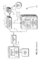
- FIG. 1A shows a block diagram of prior art mixed-signal tester 100.
- a test engineer typically develops a test program on computer work station 104, and then loads the test program into main memory 136 of test computer 102 using system bus 144.
- test computer 102 sends control signals to driver/receiver channels 108, 110, 112, and 114, and capture instruments 116, 118, 120, and 122 through test computer interface 106.
- the control signals direct driver/receiver channel 108 to receive an output signal produced by DUT 132 through tester pin 124, and send the output signal to capture instrument 116 using line 150.
- the control signals then typically direct capture instrument 116 to filter the output signal using anti-aliasing filter 155, and sample the output signal using sample-and-hold 138.
- the control signals might also direct capture instrument 116 to convert the sampled data to digital form (if necessary) using a-to-d converter 140, and store the resulting digital data in local memory 142.
- mixed-signal tester 100 may be used to analyze data derived from an output signal generated by DUT 132, we have recognized that the signal processing technique used by tester 100 yields testers which often do not have the desired performance. For example, before being sampled by sample-and-hold 138, the output signal produced by DUT 132 typically passes through either an attenuation stage (not shown) or an amplification stage (not shown) in driver/receiver channel 108.
- both the attenuation stage and the amplification stage can introduce error into output signals produced by DUT 132.
- they can introduce signal amplitude error into the output signals, thereby causing processor 134 to produce analysis results that do not have the required level of accuracy.
- Anti-aliasing filter 155 is a low-pass filter stage designed to eliminate any signal components occurring at frequencies greater than B Hz.
- anti-aliasing filter 155 can also be a source of signal amplitude error.
- anti-aliasing filters are often insufficiently flat in the passband.
- sample-and-hold 138 samples the output signal using a sampling rate that is greater than or equal to 2B Hz. Sample-and-hold 138 then presents the sampled data to a-to-d converter 140. However, both sample-and-hold 138 and a-to-d converter 140 can also be sources of signal amplitude error.
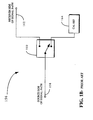
- switch 160 is actuated to connect terminal 158 to terminal 162, which is as close as possible to the end of the signal path.
- an external reference standard (not shown) is connected to terminal 162, and calibration measurements are performed by the tester.
- the external reference standard includes a series of fixed reference standards.
- Switch 160 is then actuated to connect terminal 158 to cal ref 164, which is an internal reference standard.
- Cal ref 164 also includes a series of fixed reference standards.
- the tester performs calibration measurements, and then compares them with the measurements made using the external reference standard. The difference between the calibration measurements made using the external and internal reference standards is proportional to the error introduced in the signal path. The test engineer then programs the tester to correct the error.
- a tester that can automatically correct signal amplitude error, across an entire frequency spectrum of interest, without substantially increasing test time. It would also be desirable to have a tester that has an internal calibration source that is traceable to a known standard.
- EP-A-0 699 914 describes an electronic circuit tester comprising an A/D converter including a sigma-delta modulator in series with a digital filter. The output from the A/D converter is input to a digital quantiser. A programmable calibration value is also input into the digital quantiser from a computer such that the operating level of the digital quantiser is controllable by the computer. In said tester, the calibration time is highly reduced in comparison with comparable testers.
- an electronic circuit tester as set out in Claim 1 and a method of calibrating an electronic circuit tester as set out in Claim 5.
- each channel has an input connected to a means for selecting between an output of the internal calibration source and a tester pin.
- each capture instrument has an output connected to a means for selecting between an input to a test computer and an input to the digital correction circuit.
- the internal calibration source may include a high frequency, high precision current switch.
- the digital correction circuit may include a finite impulse response (FIR) filter.
- FIR finite impulse response
- the digital correction circuit can include an FIR filter coupled in series with an infinite impulse response (IIR) filter.
- IIR infinite impulse response
- the tester calibrates the internal calibration source by measuring the amplitude of a first signal having both a predetermined amplitude and a predetermined frequency. The tester then measures the amplitude of a second signal produced by the internal calibration source and having the same frequency as the first signal. Next, the tester repetitively adjusts a bias input of the internal calibration source and repetitively measures the amplitude of the second signal until the amplitude of the second signal equals the amplitude of the first signal. The tester then stores the level of the bias input, and the values of both the predetermined amplitude and the predetermined frequency.
- the steps of measuring the amplitude of the second signal, adjusting the bias input of the internal calibration source, and storing the level of the bias input and the values of both the predetermined amplitude and the predetermined frequency, are repeated for additional predetermined frequencies. Further, this embodiment is optionally repeated for additional predetermined amplitudes of the first signal.
- the tester measures the amplitude response of its channel and data acquisition circuitry by applying a stored bias input level, corresponding to both a stored amplitude and frequency, to the internal calibration source, and measuring the amplitude of a signal produced by the internal calibration source.
- the steps of applying the stored bias input level, and measuring the amplitude of the signal produced by the internal calibration source are repeated for additional stored frequencies. Further, this embodiment is optionally repeated for additional stored amplitudes.
- the tester calculates the frequency response of the data acquisition channel using the amplitude measurements of the signal produced by the internal calibration source, thereby determining the signal amplitude error contributed by its channel and data acquisition circuitry.
- FIG. 2A shows an embodiment of a mixed-signal tester that is capable of analyzing data derived from output signals produced by an electronic circuit.
- a test engineer typically develops test programs for tester 200 on work station 202, and loads the test programs into main memory 256 of test computer 204 using system bus 264.
- the test engineer also typically enters commands for tester 200 at work station 202. For example, the test engineer may enter commands to specify certain operating parameters, and to start a test sequence. At the end of the test sequence, tester 200 sends test results to work station 202 using system bus 264 for subsequent printout or display.
- a device under test generally includes more than fifty, and likely more than one hundred pins. For this reason, tester 200 generally includes more than one hundred tester pins.
- tester pins 228, 230, 232, and 234 are each connected to different pins (not shown) on DUT 252. Further, switches 236, 238, 240, and 242 can be actuated to connect channels 212, 214, 216, and 218 to tester pins 228, 230, 232, and 234.
- Internal bus 276 connects control interface 206 to channels 212, 214, 216, and 218, and capture instruments 220, 222, 224, and 226.
- Control interface 206 typically buffers control signals passing between test computer 204, and both the driver/receiver channels and the capture instruments.
- internal bus 268 connects test computer 204 to control interface 206. Using internal buses 268 and 276, and control interface 206, test computer 204 sends both programming and control signals to the channels and the capture instruments.
- test computer 204 may send commands through control interface 206 to both channel 212 and capture instrument 220 to program them for an upcoming test.
- test computer 204 may program channel 212 to receive an output signal from DUT 252 through tester pin 228, and present the samples to capture instrument 220 using line 282.
- test computer 204 may program capture instrument 220 to filter the output signal using anti-aliasing filter 287, and sample the filtered output signal using sample-and-hold 258.
- test computer 204 may program capture instrument 220 to convert the samples from analog to digital form (if necessary) using a-to-d converter 260, and store the data samples in local memory 262.
- channel and data acquisition circuitry of a tester can contribute to signal amplitude error in signals received from a device under test.
- both the attenuation stages (not shown) and the amplification stages (not shown) commonly found in channel circuitry can introduce error into signals received from a device under test.
- An advantage of the present invention is that it gives a tester the ability to measure the signal amplitude error introduced into a signal by its channel and data acquisition circuitry, and then correct the measured signal amplitude error. This advantage is realised through the use of an adjustable internal calibration source 210, and digital filter 208.
- Digital filter 208 also preferably has a real-time throughput of 12.5 MHz. This is because data buses 266, 270, 272, and 278 also have a throughput of 12.5 MHz in the preferred embodiment.
- a benefit of the present invention is that the processing of sampled data by digital filter 208 can occur without substantially increasing the time required to move the data from local memory 262 to main memory 256. As a result, the present invention can correct signal amplitude error without increasing the time required to perform a test. Keeping testing time to a minimum is very important for testers.
- digital filter 208 might be implemented using a nnulti-rate filter bank, which consists of multiple FIR filters coupled in parallel.
- a benefit of internal calibration source 210 is that it produces a calibration signal that does not drift over time and temperature. This means that the calibration signal has good repeatability. Although components in the channel and data acquisition circuitry may drift over time and temperature, tester 200 can use the known calibration signal generated by internal calibration source 210 to measure the signal amplitude error automatically, and then correct the signal amplitude error by adjusting digital filter 208. The signal amplitude error is preferably measured and corrected just before a test, and then at regular intervals.
- test engineer can adjust internal calibration source 210 so that it produces a signal equal to a level generated by an external calibration source.
- the external calibration source is preferably traceable to a known standard. As a result, it is not necessary to connect the external calibration source to the tester each time the test engineer wishes to measure the signal amplitude error introduced by the channel and data acquisition circuitry. Instead, the test engineer can calibrate internal calibration source 210 using the external calibration source, and then use internal calibration source 210 to perform subsequent signal amplitude error measurements.
- the initializing in block 300 might change the input impedance of the channel and data acquisition circuitry, thereby introducing signal amplitude error in both the calibration signals produced by internal calibration source 210 and the signals generated by DUT 252. For this reason, the test engineer should calibrate internal calibration source 210 whenever tester 200 is initialized with a different set-up configuration. In this way, tester 200 will achieve the highest level of measurement accuracy.
- the test engineer selects both a calibration frequency value and a calibration amplitude value.
- the calibration frequency value is generally selected to be within the range of signal frequencies that tester 200 expects to receive from DUT 252.
- the selected calibration amplitude value is generally within the input voltage range of the channel and data acquisition circuitry of tester 200.
- test engineer initializes internal calibration source 210 in block 304.
- Signals CLK+ and CLK- are chosen so that internal calibration source 210 produces a signal having a frequency that is equal to the calibration frequency value selected in block 302.
- signal BIAS INPUT is chosen so that the signal generated by internal calibration source 210 has a nominal amplitude. Later in the internal calibration source calibration procedure, signal BIAS INPUT will be adjusted until the amplitude of the signal produced by internal calibration source 210 equals the calibration amplitude value selected in block 302.
- the test engineer also initializes an external calibration source in block 306.
- the external calibration source is adjusted so that it produces a signal having both the frequency and amplitude values selected in block 302.
- the external calibration source preferably produces signal levels that are traceable to a known standard.
- the test engineer then connects the external calibration source to a tester pin of tester 200 in block 308.
- This step includes actuating a switch, such as switch 236, 238, 240 or 242, to connect the tester pin to a channel, such as channel 212, 214, 216, or 218.
- tester 200 connects internal calibration source 210 to the same channel that was connected to the external calibration source in block 308.
- This step includes actuating a switch, such as switch 236, 238, 240 or 242, to connect the channel to internal calibration source 210.
- Tester 200 then measures the amplitude of the signal produced by internal calibration source 210 in block.316.
- the measurement occurring in block 316 includes the same steps as the measurement that took place in block 310.
- Blocks 304, 306, 308, 310, 312, 314, 316, 317, 318, and 320 are generally repeated for other selected calibration frequency values.
- Decision block 322 causes the procedure to loop back to block 304.
- at least fifty frequency values are selected for each amplitude value, and corresponding BIAS INPUT values are determined for each frequency/amplitude pair.
- Tester 200 subsequently uses the frequency values, along with measured amplitude values, to determine the amplitude response of the channel and data acquisition circuitry.
- Internal calibration source 210 is typically calibrated using the method shown in FIG. 3 on the factory floor before tester 200 is sent to the field. Further, the amount of time typically required to calibrate internal calibration source 210 using this method is ninety minutes.
- Tester 200 preferably determines the amplitude response of the channel and data acquisition circuitry in accordance with the procedure shown in FIG. 4.
- tester 200 connects internal calibration source 210 to a channel, in particular channel 212, 214, 216, or 218 (FIG. 2A), in block 400.
- This step includes actuating a switch, such as switch 236, 238, 240, or 242, to couple the specified channel to internal calibration source 210.
- Tester 200 then applies a stored BIAS INPUT level, corresponding to a selected frequency value, to internal calibration source 210 in block 402. This causes internal calibration source 210 to produce a signal having an amplitude that is equal to a known traceable standard, as long as internal calibration source 210 was first calibrated according to the procedure shown in FIG. 3.
- Tester 200 determines the amplitude response of the channel and data acquisition circuitry in block 410.
- Tester 200 typically uses processor 254 to calculate the amplitude gain at each selected frequency. The amplitude gain is determined using both the amplitude stored in block 320 and the amplitude stored in block 406.
- Tester 200 subsequently uses the amplitude response to correct the amplitude error introduced by the channel and data acquisition circuitry.
- the amplitude response of the channel and data acquisition circuitry is typically determined using the method shown in FIG. 4 each time tester 200 is initialized with a new set-up configuration, and then at regular intervals.
- the amount of time typically required to determine the amplitude response following this method is sixty seconds.
- tester 200 corrects the amplitude error introduced by the channel and data acquisition circuitry in accordance with the procedure shown in FIG. 5. First, tester 200 calculates a set of filter coefficients for digital filter 208 in block 500.
- tester 200 typically includes sections comprising either linear time-invariant systems or linear shift-invariant systems.
- a suitable set of filter coefficients is loaded into digital filter 208 in block 504.
- a set of filter coefficients is typically loaded into digital filter 208 between the time when a set of data samples is captured, and the time when the data samples are moved to main memory 256.
- a new set of filter coefficients is also generally loaded into digital filter 208 when the set-up configuration of tester 200 changes. The amount of time required to move 32 filter coefficients from the local memory to digital filter 208 typically does not exceed 3 ⁇ s.
- n data samples must pass through the filter in order to prepare the filter for subsequent filtering.
- This operation is commonly known as "priming" the FIR filter pipeline.
- digital filter 208 is primed to received data samples in block 506.
- the priming operation consists of moving 32 data samples through digital filter 208 at a rate of 12.5 MHz. The amount of time required to prime digital filter 208 typically does not exceed 3 ⁇ s.
- the data samples are filtered in block 508, thereby correcting the signal amplitude error introduced into the data samples by the channel and data acquisition circuitry.
- This step includes actuating a switch, such as switch 244, 246, 248, or 250, to connect the capture instrument to digital filter 208, which then presents the corrected data samples to test computer 204.
- a BIAS INPUT level along with both a corresponding selected frequency value and a measured amplitude of internal calibration source 210, are stored in main memory 256.
- this implementation is also an illustration.
- the difference between a measured amplitude of an external calibration source and the measured amplitude of internal calibration source 210 might be calculated and stored.
- digital filter 208 is an FIR filter. However, this is also merely an illustration. For example, digital filter 208 can also be implemented using an infinite impulse response (IIR) filter. Further, a digital filter comprised of an FIR stage coupled to an IIR stage might be more appropriate for certain applications.
- IIR infinite impulse response
- digital filter 208 is an FIR filter having 32 taps and 12-bit resolution.
- this implementation is also merely an illustration.
- One of skill in the art may design a digital filter having different characteristics that yields the desired performance.
Landscapes
- Physics & Mathematics (AREA)
- General Physics & Mathematics (AREA)
- Tests Of Electronic Circuits (AREA)
- Measurement Of Current Or Voltage (AREA)
Description
- FIG. 1A
- is a block diagram of a prior art mixed-signal tester that is capable of analyzing data derived from a signal produced by a DUT,
- FIG. 1B
- is a block diagram of a prior art calibration circuit that corrects signal amplitude error introduced by the channel and data acquisition circuitry of a mixed-signal tester,
- FIG. 2A
- is a block diagram of a mixed-signal tester configured according to the present invention,
- FIG. 2B
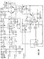
- is a detailed block diagram of the internal calibration source shown in FIG. 2A,
- FIG. 3
- is a flowchart depicting the calibration of the internal calibration source according to the present invention,
- FIG. 4
- is a flowchart depicting the measurement of the amplitude response of the channel and data acquisition circuitry according to the present invention, and
- FIG. 5
- is a flowchart depicting the correction of the channel and data acquisition circuitry according to the present invention.
Also, the filter coefficients might be calculated using the well known Parks-McClellan/Remez exchange algorithm. The amount of time typically required to calculate a set of 32 filter coefficients using this algorithm is 10 to 20 ms.
Claims (11)
- An electronic circuit tester (200) for determining whether a device under test (252) is functioning properly, including a plurality of channels (212, 214, 216, 218) with outputs coupled to respective inputs of data acquisition circuits (220, 222, 224, 226), a test computer (204) coupled to the channels and the data acquisition circuits, and
an adjustable calibration source (210) for producing a plurality of calibration signals, the calibration source being switchably connectable to each channel; and
characterised in that the tester further includes:wherein the calibration signals produced by the adjustable calibration source are used for determining signal amplitude errors contributed by the channels and the respective data acquisition circuits; anda digital filter (208), the output of said digital filter (208) being connected to the test computer and the input of said digital filter (208) being switchably connectable to the output of each data acquisition circuit;
wherein the digital filter is programmed to correct for signal amplitude errors contributed by the channels and the respective data acquisition circuits. - The electronic circuit tester as recited in claim 1, further comprising:wherein the calibration signals produced by the adjustable calibration source are established by adjusting their amplitudes to match amplitudes of signals from an external reference standard which, in use, is periodically connected to the tester pin, and are used while measuring the device under test for determining the signal amplitude errors contributed by the channels and the respective data acquisition circuits.a plurality of switches (236, 238, 240, 242), each being configurable in a first position for connecting a channel and respective data acquisition circuit to a tester pin, and in a second position for connecting the channel and respective data acquisition circuit to the adjustable calibration source, and
- The electronic circuit tester as recited in claim 1 or 2, further comprising:a first high speed data bus (272) connected between the respective data acquisition circuits and the digital filter, anda second high speed data bus (266) connected between the digital filter and the test computer.
- The electronic circuit tester as recited in claim 1, wherein the programmed digital filter is adapted for inverse filtering signals produced by the respective data acquisition circuits.
- A method of calibrating an electronic circuit tester (200), the electronic circuit tester including a plurality of channels (212, 214, 216, 218) connected to respective data acquisition circuits (220, 222, 224, 226), an adjustable calibration source (210) switchably connectable to each channel, and a digital filter (208) switchably connectable to the output of each data acquisition circuit, the method comprising the steps of:(a) calibrating the adjustable calibration source;(b) using the adjustable calibration source to produce a plurality of calibration signals, the plurality of calibration signals having specified amplitudes and specified frequencies;(c) passing the calibration signals through one of the plurality of channels and a respective data acquisition circuit, thereby distorting the calibration signals;(d) determining amplitudes of the distorted signals at the specified frequencies, thereby determining the amplitude response of the channel and the respective data acquisition circuit; and(e) programming the digital filter using the amplitude response determined in step (d), to make the overall response of the channel, the respective data acquisition circuit, and the digital filter equal to a unit sample, to correct a signal amplitude error contributed by the channels and the data acquisition circuits to at least one signal produced by a circuit under test (252).
- The method as recited in Claim 5, wherein the calibration signals of step (b) are each established by:measuring a first amplitude response of a channel and respective data acquisition circuit to an external, precision calibration standard;measuring a second amplitude response of the channel and respective data acquisition circuit to the adjustable calibration source; andadjusting the amplitude of the calibration signal from the adjustable calibration source so that the amplitude level of the second response equals that of the first response.
- The method as recited in claim 5, wherein the step of calibrating the adjustable calibration source includes the substeps of:(i) selecting an amplitude and at least one frequency;(ii) adjusting the adjustable calibration source until it produces a first signal having the frequency specified in step (i) and a nominal amplitude value;(iii) adjusting an external calibration source until it produces a second signal having the amplitude and the frequency specified in step (i);(iv) passing the second signal through the channel and the respective data acquisition circuit;(v) measuring and storing the amplitude of the signal passed in step (iv);(vi) connecting the adjustable calibration source to the channel;(vii) passing the first signal through the channel and the respective data acquisition circuit;(viii) measuring the amplitude of the first signal passed in step (vii) and adjusting the amplitude of the first signal if it is not equal to the amplitude stored in step (v) until the measured amplitude of the first signal passed in step (vii) is equal to the amplitude stored in step (v);(ix) storing an adjustment setting for making an adjustment as determined in step (viii); and(x) repeating steps (ii) - (ix) for each of said specified frequencies if more than one frequency are selected.
- The method as recited in claim 5, wherein the determining in step (d) determining amplitudes of the distorted signals includes the steps of:filtering the distorted signals;sampling the distorted signals;converting the distorted signals from analog to digital form to produce data samples; andperforming digital signal processing on the data samples.
- The method as recited in claim 5, wherein the using in step (b) includes the step of:applying a stored adjustment setting to the adjustable calibration source to produce a signal having the specified frequency and the specified amplitude.
- The method as recited in claim 5, wherein step (e) further comprises the steps of:calculating at least one set of digital filter coefficients for said digital filter;storing the set of digital filter coefficients;loading the set of digital filter coefficients into the digital filter; andfiltering a group of data samples which have been received from the respective data acquisition circuit.
- A method comprising the method of claim 5, and the further step of
passing the distorted signals through the programmed digital filter, thereby recovering the calibration signals produced in step (b).
Applications Claiming Priority (3)
| Application Number | Priority Date | Filing Date | Title |
|---|---|---|---|
| US08/760,537 US5929628A (en) | 1996-12-05 | 1996-12-05 | Apparatus and method for performing amplitude calibration in an electronic circuit tester |
| US760537 | 1996-12-05 | ||
| PCT/US1997/022408 WO1998025153A2 (en) | 1996-12-05 | 1997-12-03 | Measurement instrument amplitude calibration |
Publications (2)
| Publication Number | Publication Date |
|---|---|
| EP0941480A1 EP0941480A1 (en) | 1999-09-15 |
| EP0941480B1 true EP0941480B1 (en) | 2005-07-27 |
Family
ID=25059398
Family Applications (1)
| Application Number | Title | Priority Date | Filing Date |
|---|---|---|---|
| EP97948619A Expired - Lifetime EP0941480B1 (en) | 1996-12-05 | 1997-12-03 | Measurement instrument amplitude calibration |
Country Status (4)
| Country | Link |
|---|---|
| US (1) | US5929628A (en) |
| EP (1) | EP0941480B1 (en) |
| DE (1) | DE69733829T2 (en) |
| WO (1) | WO1998025153A2 (en) |
Families Citing this family (20)
| Publication number | Priority date | Publication date | Assignee | Title |
|---|---|---|---|---|
| DE19817763C2 (en) * | 1998-04-21 | 2001-02-15 | Texas Instruments Deutschland | Method for calibrating a measuring device |
| US6397160B1 (en) * | 1999-06-04 | 2002-05-28 | Teradyne, Inc. | Power sensor module for microwave test systems |
| US20030110427A1 (en) * | 2000-04-12 | 2003-06-12 | Advantest Corporation | Semiconductor test system storing pin calibration data in non-volatile memory |
| US20040181731A1 (en) * | 2000-04-12 | 2004-09-16 | Advantest Corporation | Semiconductor test system storing pin calibration data, commands and other data in non-volatile memory |
| US6628923B1 (en) | 2000-05-03 | 2003-09-30 | Nokia Networks Oy | Adaptive phase and amplitude linearization method and apparatus |
| DE10112304C1 (en) * | 2001-03-14 | 2002-07-18 | Siemens Ag | Measurement value acquisition and processing unit for small measurement signals |
| KR100475739B1 (en) * | 2002-12-16 | 2005-03-10 | 삼성전자주식회사 | system for testing character of filter |
| DE10330043B4 (en) * | 2003-06-30 | 2007-09-27 | Infineon Technologies Ag | System and calibration procedure |
| EP1656563B1 (en) * | 2003-08-14 | 2008-12-31 | Nxp B.V. | Calibration of tester and testboard by golden sample |
| CN100543692C (en) * | 2005-11-11 | 2009-09-23 | 鸿富锦精密工业(深圳)有限公司 | Apparatus for testing interface of video figure of computer |
| WO2008146451A1 (en) * | 2007-05-28 | 2008-12-04 | Advantest Corporation | Semiconductor testing device and testing method |
| US8310270B2 (en) * | 2007-10-04 | 2012-11-13 | Teradyne, Inc. | Emulating behavior of a legacy test system |
| US7888947B2 (en) * | 2007-11-21 | 2011-02-15 | Teradyne, Inc. | Calibrating automatic test equipment |
| US8831318B2 (en) * | 2009-07-06 | 2014-09-09 | The Board Of Trustees Of The University Of Illinois | Auto-calibrating parallel MRI technique with distortion-optimal image reconstruction |
| CN101915902B (en) * | 2010-09-06 | 2013-04-24 | 株洲南车时代电气股份有限公司 | Calibration method and calibration system for field test equipment |
| KR101517349B1 (en) | 2010-12-22 | 2015-05-04 | 주식회사 아도반테스토 | Calibration module for a tester and tester |
| US8874397B2 (en) * | 2011-01-14 | 2014-10-28 | National Instruments Corporation | User-invoked calibration of modular system using an embedded calibration signal generator |
| CN102654771B (en) * | 2012-05-16 | 2014-03-26 | 电子科技大学 | Automatic calibration method and system of analog channel |
| US11940478B2 (en) * | 2020-12-07 | 2024-03-26 | Duke University | Electronic device characterization systems and methods |
| CN114002639B (en) * | 2021-10-19 | 2022-11-01 | 华中科技大学 | Relative error self-monitoring system and method of electric signal acquisition circuit |
Family Cites Families (10)
| Publication number | Priority date | Publication date | Assignee | Title |
|---|---|---|---|---|
| DE3344251A1 (en) * | 1983-12-07 | 1985-06-20 | Siemens AG, 1000 Berlin und 8000 München | METHOD FOR TESTING LEVEL-DEPENDENT PROPERTIES OF TRANSMISSION DEVICES, ESPECIALLY THE LEVEL-DEPENDENT DAMPING DISTORTION DISTORTION OF CODECS FOR PCM DEVICES, AND APPARATUS FOR IMPLEMENTING THE METHOD |
| US4703448A (en) * | 1984-10-25 | 1987-10-27 | Nicolet Instrument Corporation | Method for measuring skew or phase difference in electronic systems |
| JPH0697256B2 (en) * | 1986-04-14 | 1994-11-30 | 株式会社アドバンテスト | AC level calibration device |
| US5184062A (en) * | 1990-05-11 | 1993-02-02 | Nicolet Instrument Corporation | Dynamically calibrated trigger for oscilloscopes |
| ATE193125T1 (en) * | 1992-03-31 | 2000-06-15 | Siemens Ag | METHOD FOR ALIGNING THE TRANSMITTING AND MEASURING CIRCUIT OF A TEST DEVICE |
| DE59510984D1 (en) * | 1994-09-05 | 2005-02-10 | Landis & Gyr Ag Zug | Arrangement for measuring electrical energy |
| US5572160A (en) * | 1994-12-01 | 1996-11-05 | Teradyne, Inc. | Architecture for RF signal automatic test equipment |
| US5548538A (en) * | 1994-12-07 | 1996-08-20 | Wiltron Company | Internal automatic calibrator for vector network analyzers |
| US5604751A (en) * | 1995-11-09 | 1997-02-18 | Teradyne, Inc. | Time linearity measurement using a frequency locked, dual sequencer automatic test system |
| US5673272A (en) * | 1996-02-13 | 1997-09-30 | Teradyne, Inc. | Apparatus and method for performing digital signal processing in an electronic circuit tester |
-
1996
- 1996-12-05 US US08/760,537 patent/US5929628A/en not_active Expired - Lifetime
-
1997
- 1997-12-03 WO PCT/US1997/022408 patent/WO1998025153A2/en not_active Ceased
- 1997-12-03 EP EP97948619A patent/EP0941480B1/en not_active Expired - Lifetime
- 1997-12-03 DE DE69733829T patent/DE69733829T2/en not_active Expired - Lifetime
Also Published As
| Publication number | Publication date |
|---|---|
| WO1998025153A2 (en) | 1998-06-11 |
| US5929628A (en) | 1999-07-27 |
| WO1998025153A3 (en) | 1998-08-27 |
| DE69733829T2 (en) | 2006-06-08 |
| EP0941480A1 (en) | 1999-09-15 |
| DE69733829D1 (en) | 2005-09-01 |
Similar Documents
| Publication | Publication Date | Title |
|---|---|---|
| US5929628A (en) | Apparatus and method for performing amplitude calibration in an electronic circuit tester | |
| EP1025450B1 (en) | Automated microwave test system with improved accuracy | |
| JP4255284B2 (en) | Single-ended channel calibration for differential operation | |
| EP0242700A2 (en) | AC level calibration method and apparatus | |
| CN102095904A (en) | Signal acquisition system having a compensation digital filter | |
| JPH0862308A (en) | Timing calibration method for measuring signal of semiconductor testing device and its circuit | |
| US8788234B2 (en) | Method of calibrating interleaved digitizer channels | |
| CN111555995B (en) | A Phase-Frequency Response Measurement and Compensation Method of a Broadband Acquisition System | |
| WO2005026759A1 (en) | Calibration comparator circuit | |
| US5604751A (en) | Time linearity measurement using a frequency locked, dual sequencer automatic test system | |
| CN114337600A (en) | On-chip differential active RC filter calibration and tuning method | |
| US4937535A (en) | Calibration method and programmable phase-gain amplifier | |
| US6981192B2 (en) | Deskewed differential detector employing analog-to-digital converter | |
| CN106970319B (en) | Method for measuring shaking-off and shaking-off time of relay | |
| CN114157297B (en) | Test device and test method for high-precision analog-to-digital conversion chip | |
| US4417310A (en) | Apparatus for measuring distortion factor | |
| US20060223440A1 (en) | Low frequency noise source and method of calibration thereof | |
| US12531566B2 (en) | Combining sampling analog-to-digital converter with continuously integrating analog-to-digital converter | |
| US20020158625A1 (en) | Test apparatus for parallel testing a number of electronic components and a method for calibrating the test apparatus | |
| US6795787B2 (en) | Method and apparatus for calibrating a sampling circuit | |
| EP4679105A1 (en) | Apparatus for testing electrical characteristics of multi-pin device | |
| JPS6214525A (en) | Analog and digital measuring instrument | |
| US20070216394A1 (en) | Measure the mutual phase relationship of a set of spectral components generated by a signal generator | |
| SU1582157A1 (en) | Method of calibrating selective measuring instruments | |
| EP1008861A1 (en) | AC calibration apparatus |
Legal Events
| Date | Code | Title | Description |
|---|---|---|---|
| PUAI | Public reference made under article 153(3) epc to a published international application that has entered the european phase |
Free format text: ORIGINAL CODE: 0009012 |
|
| 17P | Request for examination filed |
Effective date: 19990623 |
|
| AK | Designated contracting states |
Kind code of ref document: A1 Designated state(s): DE FR GB IE |
|
| 17Q | First examination report despatched |
Effective date: 20000328 |
|
| GRAP | Despatch of communication of intention to grant a patent |
Free format text: ORIGINAL CODE: EPIDOSNIGR1 |
|
| GRAA | (expected) grant |
Free format text: ORIGINAL CODE: 0009210 |
|
| GRAS | Grant fee paid |
Free format text: ORIGINAL CODE: EPIDOSNIGR3 |
|
| AK | Designated contracting states |
Kind code of ref document: B1 Designated state(s): DE FR GB IE |
|
| REG | Reference to a national code |
Ref country code: GB Ref legal event code: FG4D |
|
| REG | Reference to a national code |
Ref country code: IE Ref legal event code: FG4D |
|
| REF | Corresponds to: |
Ref document number: 69733829 Country of ref document: DE Date of ref document: 20050901 Kind code of ref document: P |
|
| ET | Fr: translation filed | ||
| PLBE | No opposition filed within time limit |
Free format text: ORIGINAL CODE: 0009261 |
|
| STAA | Information on the status of an ep patent application or granted ep patent |
Free format text: STATUS: NO OPPOSITION FILED WITHIN TIME LIMIT |
|
| 26N | No opposition filed |
Effective date: 20060428 |
|
| PGFP | Annual fee paid to national office [announced via postgrant information from national office to epo] |
Ref country code: GB Payment date: 20071227 Year of fee payment: 11 |
|
| PGFP | Annual fee paid to national office [announced via postgrant information from national office to epo] |
Ref country code: FR Payment date: 20071217 Year of fee payment: 11 |
|
| GBPC | Gb: european patent ceased through non-payment of renewal fee |
Effective date: 20081203 |
|
| PGFP | Annual fee paid to national office [announced via postgrant information from national office to epo] |
Ref country code: IE Payment date: 20071224 Year of fee payment: 11 |
|
| REG | Reference to a national code |
Ref country code: IE Ref legal event code: MM4A |
|
| REG | Reference to a national code |
Ref country code: FR Ref legal event code: ST Effective date: 20090831 |
|
| PG25 | Lapsed in a contracting state [announced via postgrant information from national office to epo] |
Ref country code: IE Free format text: LAPSE BECAUSE OF NON-PAYMENT OF DUE FEES Effective date: 20081203 |
|
| PG25 | Lapsed in a contracting state [announced via postgrant information from national office to epo] |
Ref country code: GB Free format text: LAPSE BECAUSE OF NON-PAYMENT OF DUE FEES Effective date: 20081203 |
|
| PG25 | Lapsed in a contracting state [announced via postgrant information from national office to epo] |
Ref country code: FR Free format text: LAPSE BECAUSE OF NON-PAYMENT OF DUE FEES Effective date: 20081231 |
|
| PGFP | Annual fee paid to national office [announced via postgrant information from national office to epo] |
Ref country code: DE Payment date: 20091230 Year of fee payment: 13 |
|
| REG | Reference to a national code |
Ref country code: DE Ref legal event code: R119 Ref document number: 69733829 Country of ref document: DE Effective date: 20110701 |
|
| PG25 | Lapsed in a contracting state [announced via postgrant information from national office to epo] |
Ref country code: DE Free format text: LAPSE BECAUSE OF NON-PAYMENT OF DUE FEES Effective date: 20110701 |