EP0939363B1 - Method for implementing modular multiplication according to the Montgomery method - Google Patents
Method for implementing modular multiplication according to the Montgomery method Download PDFInfo
- Publication number
- EP0939363B1 EP0939363B1 EP99470005A EP99470005A EP0939363B1 EP 0939363 B1 EP0939363 B1 EP 0939363B1 EP 99470005 A EP99470005 A EP 99470005A EP 99470005 A EP99470005 A EP 99470005A EP 0939363 B1 EP0939363 B1 EP 0939363B1
- Authority
- EP
- European Patent Office
- Prior art keywords
- register
- circuit
- word
- bits
- multiplication
- Prior art date
- Legal status (The legal status is an assumption and is not a legal conclusion. Google has not performed a legal analysis and makes no representation as to the accuracy of the status listed.)
- Expired - Lifetime
Links
Images


Classifications
-
- G—PHYSICS
- G06—COMPUTING; CALCULATING OR COUNTING
- G06F—ELECTRIC DIGITAL DATA PROCESSING
- G06F7/00—Methods or arrangements for processing data by operating upon the order or content of the data handled
- G06F7/38—Methods or arrangements for performing computations using exclusively denominational number representation, e.g. using binary, ternary, decimal representation
- G06F7/48—Methods or arrangements for performing computations using exclusively denominational number representation, e.g. using binary, ternary, decimal representation using non-contact-making devices, e.g. tube, solid state device; using unspecified devices
- G06F7/52—Multiplying; Dividing
- G06F7/523—Multiplying only
- G06F7/53—Multiplying only in parallel-parallel fashion, i.e. both operands being entered in parallel
- G06F7/5324—Multiplying only in parallel-parallel fashion, i.e. both operands being entered in parallel partitioned, i.e. using repetitively a smaller parallel parallel multiplier or using an array of such smaller multipliers
-
- G—PHYSICS
- G06—COMPUTING; CALCULATING OR COUNTING
- G06F—ELECTRIC DIGITAL DATA PROCESSING
- G06F7/00—Methods or arrangements for processing data by operating upon the order or content of the data handled
- G06F7/60—Methods or arrangements for performing computations using a digital non-denominational number representation, i.e. number representation without radix; Computing devices using combinations of denominational and non-denominational quantity representations, e.g. using difunction pulse trains, STEELE computers, phase computers
- G06F7/72—Methods or arrangements for performing computations using a digital non-denominational number representation, i.e. number representation without radix; Computing devices using combinations of denominational and non-denominational quantity representations, e.g. using difunction pulse trains, STEELE computers, phase computers using residue arithmetic
- G06F7/727—Modulo N arithmetic, with N being either (2**n)-1,2**n or (2**n)+1, e.g. mod 3, mod 4 or mod 5
-
- G—PHYSICS
- G06—COMPUTING; CALCULATING OR COUNTING
- G06F—ELECTRIC DIGITAL DATA PROCESSING
- G06F7/00—Methods or arrangements for processing data by operating upon the order or content of the data handled
- G06F7/38—Methods or arrangements for performing computations using exclusively denominational number representation, e.g. using binary, ternary, decimal representation
- G06F7/48—Methods or arrangements for performing computations using exclusively denominational number representation, e.g. using binary, ternary, decimal representation using non-contact-making devices, e.g. tube, solid state device; using unspecified devices
- G06F7/499—Denomination or exception handling, e.g. rounding or overflow
- G06F7/49931—Modulo N reduction of final result
-
- G—PHYSICS
- G06—COMPUTING; CALCULATING OR COUNTING
- G06F—ELECTRIC DIGITAL DATA PROCESSING
- G06F7/00—Methods or arrangements for processing data by operating upon the order or content of the data handled
- G06F7/60—Methods or arrangements for performing computations using a digital non-denominational number representation, i.e. number representation without radix; Computing devices using combinations of denominational and non-denominational quantity representations, e.g. using difunction pulse trains, STEELE computers, phase computers
- G06F7/72—Methods or arrangements for performing computations using a digital non-denominational number representation, i.e. number representation without radix; Computing devices using combinations of denominational and non-denominational quantity representations, e.g. using difunction pulse trains, STEELE computers, phase computers using residue arithmetic
- G06F7/722—Modular multiplication
-
- G—PHYSICS
- G06—COMPUTING; CALCULATING OR COUNTING
- G06F—ELECTRIC DIGITAL DATA PROCESSING
- G06F7/00—Methods or arrangements for processing data by operating upon the order or content of the data handled
- G06F7/60—Methods or arrangements for performing computations using a digital non-denominational number representation, i.e. number representation without radix; Computing devices using combinations of denominational and non-denominational quantity representations, e.g. using difunction pulse trains, STEELE computers, phase computers
- G06F7/72—Methods or arrangements for performing computations using a digital non-denominational number representation, i.e. number representation without radix; Computing devices using combinations of denominational and non-denominational quantity representations, e.g. using difunction pulse trains, STEELE computers, phase computers using residue arithmetic
- G06F7/728—Methods or arrangements for performing computations using a digital non-denominational number representation, i.e. number representation without radix; Computing devices using combinations of denominational and non-denominational quantity representations, e.g. using difunction pulse trains, STEELE computers, phase computers using residue arithmetic using Montgomery reduction
Definitions
- the invention relates to an implementation method a specific modular multiplication relating to the Montgomery method. More specifically, the invention concerns the improvement of the sequencing of a coprocessor modular arithmetic allowing to perform modular operations according to the Montgomery method, in order to extend the possibilities of a device having such a processor.
- the Montgomery method allows to perform modular calculations in a finite field GF (2 n ) (Galois field) without performing a division.
- D2 coprocessor allows optimize (in terms of calculation time, size memory, etc.) processing modular operations using a fixed data size, in this case 256 or 512 bits.
- a fixed data size in this case 256 or 512 bits.
- Cryptography requires machines more and more efficient, working more and more quickly and using increasingly complex keys. We is thus moving towards the manipulation of coded data on 768, 1024, 1536 and even 2048 bits.
- To deal with such data we can consider carrying out larger circuits by adapting the circuit elements at data sizes. This solution can cause problems in applications such as smart cards for which the size circuits is physically limited due to differences in mechanical bending stress between silicon card and substrate.
- circuit 1 can be used shown in Figure 1 which includes a processor classic 2 (8, 16, or 32 bit), a memory 3, a coprocessor 4, and a communication bus 5 used to connect the different elements 2, 3 and 4 together and / or outside circuit 1.
- the coprocessor 4 is then used as a multiplier working on m * k bits (conventionally 256 or 512 bits).
- Processor 2 is used to supervise in particular the operations to be performed using an encryption algorithm particular and data exchanges between memory 3 and the coprocessor 4.
- the invention also relates to a coprocessor modular arithmetic as defined in claim 7.
- the invention relates to a circuit integrated implementing modular operations according to Montgomery's method which includes a processor, a memory and the coprocessor of the invention.
- the method previously stated intelligently uses the register 111 so as to memorize simultaneously an intermediate result R i and the i + 1 words of the final result S (indeed, the word R i, 0 also coorespond to the word S i ) , the intermediate result corresponding to the m - i words of k least significant bits of the multiplication of B by A i .
- step A) is not a necessary step if the coprocessor 4 is in the state corresponding to the end of this step A) before starting the calculation.
- steps B1 and C2 depending on whether you want to shunt or not the delay cell 134.
- this process with a coprocessor with four registers of m * k bits in order to memorize fully A in coprocessor 4.
- a first improvement consists in using registers of m * k bits of variable size by words of k bits so as to reduce the number of shifts to perform during each iteration.
- the use of variable size registers can, for example, delete steps B2, C3 and C4 by varying the size of the registers during each execution of step C2.
- a second improvement consists in using the two multiplication circuits 119 and 120 simultaneously so as to reduce the calculation time.
- FIG. 3 shows a coprocessor according to the invention which makes it possible to carry out the invention with the improvements mentioned above. It is however possible to make a coprocessor according to the invention which only uses part of these improvements in depending on the different speed constraints, calculation and occupation of silicon surface and possible compromises resulting from these constraints.
- Figure 3 shows an example of a coprocessor 4b according to the invention.
- terminals can also be one or more input / output terminals common to several elements of the coprocessor.
- multiplexers can be grouped together and then include a number of inputs, outputs, and larger selection entries.
- multiplexers 225, 236, 237, 240, 250, 252 and 253 which have an input receiving a fixed signal ("0" or "1" logic)
- the register 240 makes it possible to store in the coprocessor an operand A of n bits, which allows to limit exchanges between the coprocessor and the outside and therefore save time.
- the multiplexer 246 allows to load register 217 with bits supplied by register 240, which allows to use addition circuits 219 in parallel and 220 without requiring successive loading of registers 216 and 217 with words provided to the coprocessor.
- the 241 multiplexer allows, by looping the output of register 240 on its entry, to keep permanently intact the contents of this register, when providing by shifting the words at the output of this register.
- the fourth input of multiplexer 248 can be connected directly to the output of register 210 (which is equivalent, from a functional point of view, to the connect to the output of the subtraction circuit 227, if this last receives a logical zero on its second input permanently).
- the addition circuit 251 and the multiplexer 252 allow the implementation of type A * operations B + C + D, data C and D being provided by registers 211 and 212.
- the addition circuit 251 becomes transparent when positioning the multiplexer 252 to permanently supply the logical "0" on its output.
- Multiplexer 253 is used to connect the output of the addition circuit 251 directly at the first input of the addition circuit 231, without delaying the transfer of data between these circuits through the cell to delay 234. It also provides logical zeros to the addition circuit 231.
- the delay cell 254 makes it possible to delay by k cycle time the flow of bits produced by the circuit multiplication 220.
- the delay cell 234 is not short-circuited via multiplexer 253, the cell 254 in order to obtain a delay of 2 * k time of cycle.
- the multiplexer 256 makes it possible to store in one registers 210 to 212 the bits produced by the circuit addition 230.
- Multiplexer 256 can also be deleted at condition of neutralizing the addition circuit 231 in sending "0" on its second entry via the multiplexer 255 and the multiplication circuit 248.
- shift registers 210, 211, 212 and 240 of variable size registers arranged in bank of registers as shown in Figure 3 for the register 240.
- Register 240 is made up of m sub-registers 240-1 to 240-m which are k bit shift registers each having a serial input and a serial output. The inputs are connected together to form the input of the register 240.
- a MUX multiplexer with m inputs series and a serial output at each of its inputs respectively connected to each output of the sub-registers 240-1 to 240-m.
- registers 210, 211 and 212 have been represented in a single block although they are of the same structure as the register 240, i.e. each divided into m sub-registers respectively 210-1 to 210-m, 211-1 to 211-m, 212-1 to 212-m.
- register bank allows addition to having at most 2 * k register cells which work simultaneously either a divided consumption by m / 2 when working with words of m * K bits.
- step C ' by varying i from 1 to (m-1) / 2 + 1 and adding step C "2 just before l 'stage D': C "2) an offset of k bits is carried out at the content of the sub-register 210-1 to produce A m-1 *.
- an offset of k bits is effected simultaneously at the content of the sub-register register 211-m to add in the addition circuit 230 R (m-1) / 2-1.2 to the result leaving the multiplication circuit 219 to obtain A m-1 * B 0 + R (m-1) / 2-1,2 the first word this k bits leaving the addition circuit 230 corresponding to S m-1 is stored in the sub-register 211-m.
- Variable size registers used reduce the duration of each iteration by function of the number of k-bit words of S obtained during each iteration of the process. For the effect to be obtained, it suffices that registers 210 and 211 are of variable size.
- Register 240 makes it possible to store A in full in order to suppress the exchanges between memory 3 and the coprocessor 4 during the course of the calculation. Through elsewhere, the data contained in the register 240 can be reused if the register has been looped back to itself. The use of register 240 is partially compensated in terms of area insofar as this reduces the size of the memory 3.
Landscapes
- Physics & Mathematics (AREA)
- General Physics & Mathematics (AREA)
- Engineering & Computer Science (AREA)
- Mathematical Analysis (AREA)
- Mathematical Optimization (AREA)
- Pure & Applied Mathematics (AREA)
- Computational Mathematics (AREA)
- Theoretical Computer Science (AREA)
- Computing Systems (AREA)
- General Engineering & Computer Science (AREA)
- Mathematical Physics (AREA)
- Logic Circuits (AREA)
- Complex Calculations (AREA)
Description
L'invention concerne un procédé de mise en oeuvre d'une multiplication modulaire spécifique relative à la méthode de Montgomery. Plus précisément, l'invention concerne l'amélioration du séquencement d'un coprocesseur d'arithmétique modulaire permettant de réaliser des opérations modulaires selon la méthode de Montgomery, afin d'étendre les possibilités d'un dispositif comportant un tel processeur.The invention relates to an implementation method a specific modular multiplication relating to the Montgomery method. More specifically, the invention concerns the improvement of the sequencing of a coprocessor modular arithmetic allowing to perform modular operations according to the Montgomery method, in order to extend the possibilities of a device having such a processor.
La méthode de Montgomery permet d'effectuer des calculs modulaires dans un corps fini GF(2n) (corps de Galois) sans effectuer de division.The Montgomery method allows to perform modular calculations in a finite field GF (2 n ) (Galois field) without performing a division.
Classiquement, les opérations modulaires sur GF(2n) sont utilisées en cryptographie pour des applications telles que l'authentification de messages, l'identification d'un utilisateur et l'échange de clés. De tels exemples d'applications sont décrits par exemple dans un document Dl correspondant à la demande de brevet FR-A-2 679 054.Conventionally, modular operations on GF (2 n ) are used in cryptography for applications such as message authentication, user identification and key exchange. Examples of such applications are described for example in a document Dl corresponding to patent application FR-A-2 679 054.
On trouve dans le commerce des circuits intégrés dédiés à de telles applications, par exemple le produit fabriqué par la société SGS-THOMSON Microelectronics et portant la référence ST16CF54, bâti autour d'une association de type unité centrale - coprocesseur arithmétique, et dédié à la mise en oeuvre de calculs modulaires. Le coprocesseur utilisé permet de traiter des opérations modulaires en utilisant la méthode de Montgomery. Il fait l'objet de la demande de brevet EP-A-0 601-907 que l'on appellera par la suite le document D2.There are commercially available integrated circuits dedicated to such applications, for example the product manufactured by SGS-THOMSON Microelectronics and bearing the reference ST16CF54, built around a CPU type association - coprocessor arithmetic, and dedicated to the implementation of calculations modular. The coprocessor used makes it possible to process modular operations using the method of Montgomery. It is the subject of patent application EP-A-0 601-907 which will be called document D2 thereafter.
L'opération de base de Montgomery (appelée Pfield) mise en oeuvre par ce coprocesseur consiste, à partir de trois données binaires A (multiplicande), B (multiplieur), et N (modulo), codées sur un nombre entier n de bits, à produire une donnée binaire Pfield(A, B)N codée sur n bits, telle que Pfield(A, B)N = A * B * I mod N. I est une donnée binaire, appelée erreur, codée sur n bits tels que I = 2-n mod N (plus précisément, la valeur de I dépend du nombre de blocs de k bits considérés pour le codage de A, k étant un entier). Pour réaliser l'opération A * B * I mod N, on considère que les données sont codées sur m mots de k bits (m et k étant des nombres entiers), avec m * k = n.The basic Montgomery operation (called Pfield) implemented by this coprocessor consists, from three binary data A (multiplicand), B (multiplier), and N (modulo), coded on an integer n of bits, to produce binary data P field (A, B) N coded on n bits, such that P field (A, B) N = A * B * I mod N. I is a binary data, called error, coded on n bits such that I = 2 -n mod N (more precisely, the value of I depends on the number of blocks of k bits considered for the coding of A, k being an integer). To carry out the operation A * B * I mod N, it is considered that the data are coded on m words of k bits (m and k being whole numbers), with m * k = n.
Dans le document D2, le coprocesseur travaille avec k = 32 et m = 8 ou 16. Le coprocesseur de D2 peut être utilisé pour produire le résultat de la multiplication modulaire A * B mod N. La multiplication modulaire se décompose en deux opérations élémentaires Pfield successives. On calcule Pfield(Pfield(A, B)N, H)N, avec H une donnée codée sur -n bits, appelée paramètre de correction d'erreur, et égale à 22n mod N. Pour de plus amples détails sur la mise en oeuvre de la multiplication modulaire, on pourra se reporter au document D2.In document D2, the coprocessor works with k = 32 and m = 8 or 16. The coprocessor of D2 can be used to produce the result of the modular multiplication A * B mod N. The modular multiplication breaks down into two elementary operations Pfield successive. We calculate P field (P field (A, B) N , H) N , with H a data coded on -n bits, called error correction parameter, and equal to 2 2n mod N. For more details on the implementation of modular multiplication, reference may be made to document D2.
L'utilisation du coprocesseur de D2 permet d'optimiser (en terme de durée de calcul, de taille mémoire, etc.) le traitement d'opérations modulaires utilisant une taille de donnée fixée, en l'occurrence 256 ou 512 bits. Or, la cryptographie nécessite des machines de plus en plus performantes, travaillant de plus en plus vite et utilisant des clefs de plus en plus complexes. On s'oriente ainsi vers la manipulation de données codées sur 768, 1024, 1536 et même 2048 bits. Pour traiter de telles données, on peut envisager de réaliser des circuits de dimensions plus importantes en adaptant les éléments du circuit aux tailles des données. Cette solution peut poser des problèmes dans des applications telles que les cartes à puce pour lesquelles la taille des circuits est physiquement limitée à cause des différences de contrainte mécanique de flexion entre carte et substrat de silicium. De plus, il est demandé d'intégrer de plus en plus d'éléments fonctionnels différents sur une telle carte et la place disponible pour un circuit de cryptage en est d'autant plus réduite. Il faut donc trouver des solutions permettant de limiter l'augmentation de la taille de ce circuit, tout en permettant de fonctionner de manière optimum pour des données de taille supérieure à la taille des registres prévus initialement.Using the D2 coprocessor allows optimize (in terms of calculation time, size memory, etc.) processing modular operations using a fixed data size, in this case 256 or 512 bits. Now cryptography requires machines more and more efficient, working more and more quickly and using increasingly complex keys. We is thus moving towards the manipulation of coded data on 768, 1024, 1536 and even 2048 bits. To deal with such data, we can consider carrying out larger circuits by adapting the circuit elements at data sizes. This solution can cause problems in applications such as smart cards for which the size circuits is physically limited due to differences in mechanical bending stress between silicon card and substrate. In addition, it is requested to integrate more and more functional elements different on such a card and the space available for an encryption circuit is all the more reduced. Solutions must therefore be found to limit increasing the size of this circuit, while allowing to work optimally for data larger than the size of the registers originally planned.
Pour réaliser des opérations modulaires utilisant des opérandes d'une taille supérieure à ce que gère le coprocesseur (c'est-à-dire en pratique de la taille maximale des registres), on peut utiliser le circuit 1 représenté sur la figure 1 qui comporte un processeur classique 2 (8, 16, ou 32 bits), une mémoire 3, un coprocesseur 4, et un bus de communication 5 servant à relier les différents éléments 2, 3 et 4 ensemble et/ou à l'extérieur du circuit 1. Dans le circuit 1 de la figure 1, le coprocesseur 4 est alors utilisé comme multiplieur travaillant sur m * k bits (classiquement 256 ou 512 bits). Le processeur 2 sert à superviser notamment les opérations à réaliser suivant un algorithme de cryptage particulier et les échanges de données entre la mémoire 3 et le coprocesseur 4.To perform modular operations using operands larger than what the coprocessor (i.e. in practice size maximum of registers), circuit 1 can be used shown in Figure 1 which includes a processor classic 2 (8, 16, or 32 bit), a memory 3, a coprocessor 4, and a communication bus 5 used to connect the different elements 2, 3 and 4 together and / or outside circuit 1. In circuit 1 in figure 1, the coprocessor 4 is then used as a multiplier working on m * k bits (conventionally 256 or 512 bits). Processor 2 is used to supervise in particular the operations to be performed using an encryption algorithm particular and data exchanges between memory 3 and the coprocessor 4.
Or la réalisation de l'opération de base des
calculs modulaires selon la méthode de Montgomery, dite
Pfield, consiste, à partir de trois données binaires A
(multiplicande), B (multiplieur) et N (modulo), codées
sur un nombre entier n de bits, à produire une donnée
binaire notée P(A, B)N codée sur n bits, telle que P(A,
B)N = A * B * I mod N, I étant une erreur due à la
méthode de Montgomery. Dans le cas où n est de taille
supérieure à la taille des registres, c'est à dire m * k,
il convient de décomposer n en p mots de Bt bits, Bt
étant une base de travail de taille inférieure ou égale à
m * k, par exemple m * k. La méthode de Montgomery se
déroule ainsi, i étant un indice variant de 0 à m - l, on
répète m fois la boucle de calcul suivante:
Un tel procédé de calcul nécessite un grand nombre d'échanges de données entre le coprocesseur 4 et la mémoire 3 et nécessite un dimensionnement de la mémoire 3 en fonction des données à mémoriser lors des calculs intermédiaires. Dans la demande de brevet EP-A-0 793 165, appelée par la suite D3, il est expliqué comment faire des multiplications non modulaires et des opérations du type S = A * B + C ou S = A * B + C + D, dans lesquelles A, B, C et D sont codées sur Bt bits avec Bt égal au plus à m * k, S étant codé sur 2 * Bt bits.Such a calculation method requires a large number data exchange between the coprocessor 4 and the memory 3 and requires sizing memory 3 according to the data to be stored during the calculations intermediaries. In patent application EP-A-0 793 165, subsequently called D3, it is explained how to do non-modular multiplications and operations of the type S = A * B + C or S = A * B + C + D, in which A, B, C and D are coded on Bt bits with Bt equal to at most at m * k, S being coded on 2 * Bt bits.
Si l'on développe l'algorithme de Montgomery
réalisé à partir d'opérations élémentaires de type S = A
* B + C + D, on obtient la répétition de la boucle de
calcul suivante:


On peut remarquer que le calcul de Y0 = (X * J0) mod 2Bt, est réalisé à partir d'une opération non modulaire qui calcul Y'1Y0. L'opération modulo 2Bt se fait ensuite par abandon du mot de poids fort de Bt bits Y'1. La mise en oeuvre du calcul de Y0 revient à faire le calcul inutile de Y'1.We can notice that the calculation of Y 0 = (X * J 0 ) mod 2 Bt , is carried out from a non-modular operation which calculates Y ' 1 Y 0 . The modulo 2 Bt operation is then done by abandoning the most significant word of Bt bits Y ' 1 . The implementation of the calculation of Y 0 amounts to making the unnecessary calculation of Y ' 1 .
L'invention propose de mettre en oeuvre l'opération Y0 = (X * J0) mod 2Bt de manière directe à l'intérieur du coprocesseur 4 afin de libérer un registre de Bt = m * k bits à l'intérieur du coprocesseur 4, le registre ainsi libéré permettant de mémoriser une donnée pendant le calcul de Y0.The invention proposes to implement the operation Y 0 = (X * J 0 ) mod 2 Bt directly inside the coprocessor 4 in order to free a register of Bt = m * k bits inside the coprocessor 4, the register thus released making it possible to memorize a datum during the calculation of Y 0 .
L'invention a pour objet un procédé de mise en oeuvre d'une opération modulaire du type S = A * B mod 2m*k, A, B et S étant codés sur au plus m mots de k bits, m et k étant des entiers supérieurs à 1, procédé qui est défini dans la revendication 1. The subject of the invention is a method of implementing a modular operation of the type S = A * B mod 2 m * k , A, B and S being coded on at most m words of k bits, m and k being integers greater than 1, a method which is defined in claim 1.
L'invention porte également sur un coprocesseur d'arithmétique modulaire tel que defini dans la revendication 7. The invention also relates to a coprocessor modular arithmetic as defined in claim 7.
Des modes de réalisation particuliers de l'invention sont spécifiés dans les revendications dépendantes attenantes.Particular embodiments of the invention are specified in the accompanying dependent claims.
Plus généralement, l'invention porte sur un circuit intégré mettant en oeuvre des opérations modulaires selon la méthode de Montgomery qui comporte un processeur, une mémoire et le coprocesseur de l'invention.More generally, the invention relates to a circuit integrated implementing modular operations according to Montgomery's method which includes a processor, a memory and the coprocessor of the invention.
L'invention sera mieux comprise et d'autres
particularités et avantages apparaítront à la lecture de
la description qui va suivre, la description faisant
référence aux dessins annexés parmi lesquels:
- trois registres à décalage 110, 111 et 112 à entrée série et sortie série, ces registres comportant un nombre n (n entier) de cellules, avec n = m * k (m et k entiers) ;
- un multiplexeur 113 comprenant trois entrées séries et une sortie série, la sortie série étant reliée à l'entrée du registre 110, la première entrée étant reliée à une première borne d'entrée 150, la deuxième entrée étant reliée à la sortie du registre 110;
- un multiplexeur 114 comprenant trois entrées séries et une sortie série, la sortie série étant reliée à l'entrée du registre 111, la première entrée étant reliée à une deuxième borne d'entrée 151, la troisième entrée étant reliée à la sortie du registre 111;
- un multiplexeur 115 comprenant trois entrées séries et une sortie série, la sortie série étant reliée à l'entrée du registre 112, la première entrée étant reliée à une troisième borne d'entrée 152, la deuxième entrée étant reliée à la sortie du registre 112;
- trois registres 116, 117 et 118 de k cellules comprenant une entrée série et une sortie parallèle, l'entrée du registre 117 étant reliée à une quatrième borne d'entrée 153;
- deux circuits 119 et 120 de multiplication comprenant une entrée série, une entrée parallèle pour recevoir k bits, et une sortie série;
- deux registres 121 et 122 de mémorisation de k cellules comprenant une entrée parallèle et une sortie parallèle, l'entrée du registre 121 étant reliée à la sortie du registre 116, la sortie du registre 121 étant reliée à l'entrée parallèle du circuit de multiplication 119, et la sortie du registre 122 étant reliée à l'entrée parallèle du circuit de multiplication 120;
- un multiplexeur 123 comprenant deux entrées parallèles et une sortie parallèle, la première entrée du multiplexeur 123 étant reliée à la sortie du registre 117, la deuxième entrée du multiplexeur 123 étant reliée à la sortie du registre 118, la sortie du multiplexeur 123 étant reliée à l'entrée du registre 122;
- deux multiplexeurs 124 et 125 comprenant chacun deux entrées séries et une sortie série, la sortie du multiplexeur 124 étant reliée à l'entrée du registre 116, la première entrée du multiplexeur 124 étant reliée à une cinquième borne d'entrée 154, la sortie du multiplexeur 125 étant reliée à l'entrée série du circuit de multiplication 119, la première entrée du multiplexeur 125 recevant un zéro logique;
- un multiplexeur 126 comprenant trois entrées séries et une sortie série, la sortie étant reliée à l'entrée série du circuit de multiplication 120, la première entrée recevant un zéro logique;
- des circuits 127, 128 et 129 de soustraction comprenant chacun deux entrées séries et une sortie série, la première entrée du circuit 127 étant reliée à la sortie du registre 110, la sortie du circuit 127 étant reliée à chacune des deuxièmes entrées des multiplexeurs 124 et 125 et également à une borne de sortie 155, la première entrée du circuit 128 étant reliée à la sortie du registre 111;
- un circuit 130 d'addition comprenant deux entrées séries et une sortie série, la première entrée du circuit 130 étant reliée à la sortie du circuit 119, la sortie du circuit 130 étant reliée à la deuxième entrée du multiplexeur 126;
- un circuit 131 d'addition comprenant deux entrées séries, une sortie série et une sortie de retenue, la sortie de retenue du circuit 131 étant reliée à la première entrée du circuit 129;
- des cellules à retard 132, 133 et 134 pour retarder de k temps de cycle la propagation de données binaires (ces cellules étant typiquement des registres à décalage de k bits), ces cellules comprenant une entrée série et une sortie série, la sortie de la cellule 132 étant reliée d'une part à la troisième entrée du multiplexeur 126 et d'autre part à l'entrée de la cellule 133, la sortie de la cellule 133 étant reliée à la deuxième entrée du circuit 129, l'entrée de la cellule 134 étant reliée à la sortie du circuit 130, et la sortie de la cellule 134 étant reliée à la première entrée du circuit 131;
- un circuit 135 de comparaison comprenant deux entrées séries et deux sorties, la première entrée étant reliée à la sortie du circuit 131, la deuxième entrée étant reliée à la sortie du circuit 129;
- deux multiplexeurs 136 et 137 comprenant chacun deux entrées séries, une entrée de sélection, et une sortie série, chacune des premières entrées recevant un zéro logique, chacune des entrées de sélection étant reliée à l'une des sorties du circuit 135, la sortie du multiplexeur 136 étant reliée à la deuxième entrée du circuit 127, la sortie du multiplexeur 137 étant reliée à la deuxième entrée du circuit 128;
- un multiplexeur 138 comprenant deux entrées séries et une sortie série, la première entrée recevant un "un" logique, la deuxième entrée étant reliée à la sortie du registre 112, la sortie étant reliée d'une part à l'entrée de la cellule 132 et d'autre part aux deuxièmes entrées des multiplexeurs 136 et 137;
- un démultiplexeur 139 comprenant une entrée série et deux sorties séries, l'entrée étant reliée à la sortie du circuit 120, les sorties étant reliées respectivement à l'entrée du registre 118 et à la deuxième entrée du circuit 131;
- un multiplexeur 140 comprenant deux entrées séries et une sortie série, la première entrée étant reliée à la sortie du circuit 128, la deuxième entrée étant reliée à un zéro logique, et la sortie étant reliée à la deuxième entrée du circuit 130;
- un multiplexeur 141 comprenant deux entrées séries et une sortie série, la première entrée étant reliée à la sortie du circuit 130, la deuxième entrée étant reliée à la sortie du circuit 131, et la sortie étant reliée aux troisièmes entrées des multiplexeurs 113 et 115 et à la deuxième entrée du multiplexeur 114;
- deux bornes de sortie 156 et 157 reliées respectivement aux sorties des registres 111 et 112.
- three shift registers 110, 111 and 112 with serial input and serial output, these registers comprising a number n (n integer) of cells, with n = m * k (m and k integers);
- a multiplexer 113 comprising three serial inputs and a serial output, the serial output being connected to the input of the register 110, the first input being connected to a first input terminal 150, the second input being connected to the output of the register 110 ;
- a multiplexer 114 comprising three serial inputs and a serial output, the serial output being connected to the input of the register 111, the first input being connected to a second input terminal 151, the third input being connected to the output of the register 111 ;
- a multiplexer 115 comprising three serial inputs and a serial output, the serial output being connected to the input of the register 112, the first input being connected to a third input terminal 152, the second input being connected to the output of the register 112 ;
- three registers 116, 117 and 118 of k cells comprising a serial input and a parallel output, the input of register 117 being connected to a fourth input terminal 153;
- two multiplication circuits 119 and 120 comprising a serial input, a parallel input for receiving k bits, and a serial output;
- two registers 121 and 122 for storing k cells comprising a parallel input and a parallel output, the input of register 121 being connected to the output of register 116, the output of register 121 being connected to the parallel input of the multiplication circuit 119, and the output of register 122 being connected to the parallel input of the multiplication circuit 120;
- a multiplexer 123 comprising two parallel inputs and a parallel output, the first input of the multiplexer 123 being connected to the output of the register 117, the second input of the multiplexer 123 being connected to the output of the register 118, the output of the multiplexer 123 being connected to entry in register 122;
- two multiplexers 124 and 125 each comprising two serial inputs and a serial output, the output of the multiplexer 124 being connected to the input of the register 116, the first input of the multiplexer 124 being connected to a fifth input terminal 154, the output of the multiplexer 125 being connected to the serial input of the multiplication circuit 119, the first input of the multiplexer 125 receiving a logic zero;
- a multiplexer 126 comprising three serial inputs and a serial output, the output being connected to the serial input of the multiplication circuit 120, the first input receiving a logic zero;
- subtraction circuits 127, 128 and 129 each comprising two serial inputs and a serial output, the first input of circuit 127 being connected to the output of register 110, the output of circuit 127 being connected to each of the second inputs of multiplexers 124 and 125 and also to an output terminal 155, the first input of circuit 128 being connected to the output of register 111;
- an addition circuit 130 comprising two serial inputs and a serial output, the first input of circuit 130 being connected to the output of circuit 119, the output of circuit 130 being connected to the second input of multiplexer 126;
- an addition circuit 131 comprising two serial inputs, a serial output and a holding output, the holding output of the circuit 131 being connected to the first input of the circuit 129;
- delay cells 132, 133 and 134 for delaying the propagation of binary data by k cycle times (these cells typically being shift registers of k bits), these cells comprising a serial input and a serial output, the output of the cell 132 being connected on the one hand to the third input of multiplexer 126 and on the other hand to the input of cell 133, the output of cell 133 being connected to the second input of circuit 129, the input of cell 134 being connected to the output of circuit 130, and the output of cell 134 being connected to the first input of circuit 131;
- a comparison circuit 135 comprising two serial inputs and two outputs, the first input being connected to the output of circuit 131, the second input being connected to the output of circuit 129;
- two multiplexers 136 and 137 each comprising two serial inputs, a selection input and a serial output, each of the first inputs receiving a logic zero, each of the selection inputs being connected to one of the outputs of circuit 135, the output of the multiplexer 136 being connected to the second input of circuit 127, the output of multiplexer 137 being connected to the second input of circuit 128;
- a multiplexer 138 comprising two serial inputs and a serial output, the first input receiving a logic "one", the second input being connected to the output of register 112, the output being connected on the one hand to the input of cell 132 and on the other hand to the second inputs of the multiplexers 136 and 137;
- a demultiplexer 139 comprising a serial input and two serial outputs, the input being connected to the output of circuit 120, the outputs being connected respectively to the input of register 118 and to the second input of circuit 131;
- a multiplexer 140 comprising two serial inputs and a serial output, the first input being connected to the output of circuit 128, the second input being connected to a logic zero, and the output being connected to the second input of circuit 130;
- a multiplexer 141 comprising two serial inputs and a serial output, the first input being connected to the output of the circuit 130, the second input being connected to the output of the circuit 131, and the output being connected to the third inputs of the multiplexers 113 and 115 and at the second input of the multiplexer 114;
- two output terminals 156 and 157 connected respectively to the outputs of registers 111 and 112.
Pour pouvoir réaliser les opérations modulaires et non modulaires citées précédemment, l'homme du métier peut se reporter entre autre à D2 et D3.To be able to carry out modular operations and non-modular mentioned above, the skilled person can refer to D2 and D3 among others.
Pour mettre en oeuvre l'opération S = A * B mod
2Bt, A, B et S étant codés sur Bt bits, Bt étant au plus
égal à m * k bits, on manipule les opérandes A, B et S en
les divisant en m sous-opérandes de k bits : Am-1...A0,
Bm-1...B0, Sm-1...S0, l'indice 0 désignant le mot de
poids le plus faible et l'indice m-1 désignant le mot de
poids le plus fort. On notera que A et B pourront avoir
en pratique des tailles différentes. On suppose ici, pour
simplifier, que A et B ont la même taille. On procède de
la manière suivante:
on charge B dans le registre 110, on initialise à "0" le registre 111, on charge A0 dans le registre 121 par l'intermédiaire du registre 116, on positionne de manière fixe les multiplexeurs 136 et 137 de manière à obtenir "0" en sortie afin de neutraliser les -circuits de soustraction 127 et 128, on positionne le multiplexeur 141 de manière fixe pour relier en permanence à sa sortie la sortie du circuit d'addition 130, on initialise les circuits d'addition 130 et de multiplication 119;
load B into register 110, initialize register "0" to 111, load A 0 into register 121 via register 116, set multiplexers 136 and 137 in a fixed manner so as to obtain "0 "at the output in order to neutralize the subtraction circuits 127 and 128, the multiplexer 141 is positioned in a fixed manner so as to permanently connect the output of the addition circuit 130 to its output, the addition circuits 130 and multiplication are initialized 119;
Dans le cas où les données A et B ne sont pas d'une même taille multiple de k, on complète le poids fort de ces données par des "0" pour obtenir deux nombres de taille identique. On peut utiliser des registres configurables en registres de taille m' * k bits < m * k bits pour traiter des mots de taille inférieure, on utilisera alors le même procédé avec des registres de taille m' * k bits au lieu de m * k bits en remplaçant m par m' dans le procédé décrit précédemment.In case data A and B are not of a same multiple size of k, we complete the high weight of this data by "0" to get two numbers of identical size. We can use registers configurable in registers of size m '* k bits <m * k bits to process smaller words, we will then use the same process with registers of size m '* k bits instead of m * k bits replacing m by m 'in the method described above.
On peut remarquer que le procédé énoncé précédemment utilise intelligemment le registre 111 de manière à mémoriser simultanément un résultat intermédiaire Ri et les i + 1 mots du résultat final S (en effet, le mot Ri,0 coorespond également au mot Si), le résultat intermédiaire correspondant aux m - i mots de k bits de poids faible de la multiplication de B par Ai. Un tel procédé permet d'utiliser le registre 112 pour mémoriser ou de charger une autre donnée pendant la réalisation de l'opération S = A * B mod 2m*k.It can be noted that the method previously stated intelligently uses the register 111 so as to memorize simultaneously an intermediate result R i and the i + 1 words of the final result S (indeed, the word R i, 0 also coorespond to the word S i ) , the intermediate result corresponding to the m - i words of k least significant bits of the multiplication of B by A i . Such a method makes it possible to use register 112 to store or load other data during the performance of the operation S = A * B mod 2 m * k .
De nombreuses variantes et améliorations sont possibles à partir de ce procédé de base. Ainsi, l'étape d'initialisation A) n'est pas une étape nécessaire si le coprocesseur 4 se trouve dans l'état correspondant à la fin de cette étape A) avant de commencer le calcul. De même, plusieurs chemins sont possibles pour réaliser les étapes B1 et C2, suivant que l'on désire shunter ou non la cellule à retard 134. Il est également possible d'utiliser ce procédé avec un coprocesseur disposant de quatre registres de m * k bits afin de mémoriser intégralement A dans le coprocesseur 4.Many variations and improvements are possible from this basic process. So the step A) is not a necessary step if the coprocessor 4 is in the state corresponding to the end of this step A) before starting the calculation. Of even, several paths are possible to achieve the steps B1 and C2, depending on whether you want to shunt or not the delay cell 134. It is also possible to use this process with a coprocessor with four registers of m * k bits in order to memorize fully A in coprocessor 4.
Une première amélioration consiste à utiliser des registres de m * k bits de taille variable par mots de k bits de manière à réduire le nombre de décalages à effectuer au cours de chaque itération. L'utilisation de registres de taille variable peut, par exemple, supprimer les étapes B2, C3 et C4 en faisant varier la taille des registres lors de chaque exécution de l'étape C2.A first improvement consists in using registers of m * k bits of variable size by words of k bits so as to reduce the number of shifts to perform during each iteration. The use of variable size registers can, for example, delete steps B2, C3 and C4 by varying the size of the registers during each execution of step C2.
Une deuxième amélioration consiste à utiliser les deux circuits de multiplication 119 et 120 simultanément de manière à réduire le temps de calcul.A second improvement consists in using the two multiplication circuits 119 and 120 simultaneously so as to reduce the calculation time.
Le schéma de la figure 3 représente un coprocesseur selon l'invention qui permet de réaliser l'invention avec les améliorations citées précédemment. Il est toutefois possible de réaliser un coprocesseur selon l'invention qui n'utilise qu'une partie de ces améliorations en fonction des différentes contraintes de rapidité, de calcul et d'occupation de surface de silicium et des compromis possibles résultant de ces contraintes.The diagram in Figure 3 shows a coprocessor according to the invention which makes it possible to carry out the invention with the improvements mentioned above. It is however possible to make a coprocessor according to the invention which only uses part of these improvements in depending on the different speed constraints, calculation and occupation of silicon surface and possible compromises resulting from these constraints.
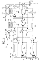
La figure 3 représente un exemple de coprocesseur 4b selon l'invention.Figure 3 shows an example of a coprocessor 4b according to the invention.
Le dispositif illustré sur la figure 3 comprend :
- quatre registres à décalage 210, 211, 212 et 240 à entrée série et sortie série, ces registres comportant un nombre n (n entier) de cellules, avec n = m * k (m et k entiers) ;
- un multiplexeur 241 comprenant deux entrées séries et une sortie série, la sortie série du multiplexeur 241 étant reliée à l'entrée du registre 240, une première entrée du multiplexeur 241 étant reliée à une première borne d'entrée 242 et une deuxième entrée du multiplexeur 241 étant reliée à la sortie du registre 240;
- un multiplexeur 213 comprenant trois entrées séries et une sortie série, la sortie série du multiplexeur 213 étant reliée à l'entrée du registre 210, une première entrée du multiplexeur 213 étant reliée à une deuxième borne d'entrée 243 et une deuxième entrée du multiplexeur 213 étant reliée à la sortie du registre 210;
- un multiplexeur 214 comprenant deux entrées séries et une sortie série, la sortie série du multiplexeur 214 étant reliée à l'entrée du registre 211, et une première entrée du multiplexeur 214 étant reliée à une troisième borne d'entrée 244;
- un multiplexeur 215 comprenant trois entrées séries et une sortie série, la sortie série du multiplexeur 215 étant reliée à l'entrée du registre 212, une première entrée du multiplexeur 215 étant reliée à une quatrième borne d'entrée 245 et une deuxième entrée du multiplexeur 215 étant reliée à la sortie du registre 212;
- trois registres 216, 217 et 218 de k cellules comprenant une entrée série et une sortie parallèle,
- un multiplexeur 246 comprenant deux entrées séries et une sortie série, la sortie série du multiplexeur 246 étant reliée à l'entrée du registre 217, une première entrée du multiplexeur 246 étant reliée à une cinquième borne d'entrée 247 et une deuxième entrée du multiplexeur 246 étant reliée à la sortie du registre 240;
- deux circuits 219 et 220 de multiplication comprenant une entrée série, une entrée parallèle pour recevoir k bits et une sortie série,
- deux registres 221 et 222 de mémorisation de k cellules comprenant une entrée et une sortie parallèles, l'entrée du registre 221 étant reliée à la sortie du registre 216, la sortie du registre 221 étant reliée à l'entrée parallèle du circuit de multiplication 219 et la sortie du registre 222 étant reliée à l'entrée parallèle du circuit de multiplication 220;
- un multiplexeur 223 comprenant deux entrées parallèles et une sortie parallèle, une première entrée du multiplexeur 223 étant reliée à la sortie du registre 217 et une deuxième entrée du multiplexeur 223 étant reliée à la sortie du registre 218, la sortie du multiplexeur 223 étant reliée à l'entrée du registre 222;
- deux multiplexeurs 224 et 225 comprenant chacun deux entrées séries et une sortie série, la sortie du multiplexeur 224 étant reliée à l'entrée du registre 216, une première entrée du multiplexeur 224 étant reliée à la sortie du registre 240, la sortie du multiplexeur 225 étant reliée à l'entrée série du circuit de multiplication 219 et une première entrée du multiplexeur 225 recevant un "0" logique;
- un multiplexeur 248 comprenant quatre entrées série et une sortie série, la sortie du multiplexeur 248 étant reliée à l'entrée série du circuit de multiplication 220 et une première entrée de ce multiplexeur recevant un "0" logique;
- des circuits de soustraction 227, 228 et 229 comprenant chacun deux entrées séries et une sortie série, une première entrée du circuit 227 étant reliée à la sortie du registre 210, la sortie du circuit 227 étant reliée à chacune des deuxièmes entrées des multiplexeurs 224 et 225, à une borne de sortie 249 et à une quatrième entrée du multiplexeur 248;
- un multiplexeur 250 comprenant deux entrées série et une sortie série, la sortie du multiplexeur 250 étant reliée à une première entrée du circuit 228, une première entrée du multiplexeur 250 étant reliée à la sortie du registre 211 et une deuxième entrée de ce multiplexeur recevant un "0" logique;
- trois circuits d'addition 230, 231 et 251 comprenant chacun deux entrées séries et une sortie série, une première entrée du circuit 230 étant reliée à la sortie du circuit 219 et une deuxième entrée de ce circuit étant reliée à la sortie du circuit de soustraction 228, la sortie du circuit 230 étant reliée d'une part à une deuxième entrée du multiplexeur 248 et d'autre part à une première entrée du circuit 251, la sortie du circuit 231 étant reliée à une première entrée du circuit 229;
- un multiplexeur 252 comprenant deux entrées séries et une sortie série, la sortie du multiplexeur 252 étant reliée à une deuxième entrée du circuit d'addition 251, une première entrée du multiplexeur 252 étant reliée à la sortie du registre 212 et une deuxième entrée de ce multiplexeur recevant un "0" logique;
- un multiplexeur 253 comprenant trois entrées séries et une sortie série, la sortie série du multiplexeur 253 étant reliée à une première entrée du circuit d'addition 231 et une première entrée de ce multiplexeur étant reliée à la sortie du circuit d'addition 251, la troisième entrée du multiplexeur recevant un "0" logique;
- des cellules à retard 232, 233 et 234 pour retarder de k temps de cycle la propagation de données binaires (ces cellules étant typiquement des registres à décalage de k bits, c'est-à-dire de la taille des registres 216, 217 et 218), ces cellules comprenant une entrée série et une sortie série, la sortie de la cellule 232 étant reliée d'une part à une troisième entrée du multiplexeur 248 et d'autre part à l'entrée de la cellule 233, la sortie de la cellule 233 étant reliée à une deuxième entrée du circuit 229, l'entrée de la cellule 234 étant reliée à la sortie du circuit d'addition 251 et la sortie de la cellule 234 étant reliée à une deuxième entrée du multiplexeur 253;
- un circuit 235 de comparaison comprenant deux entrées séries et deux sorties, une première entrée du circuit 235 étant reliée à la sortie du circuit 231 et une deuxième entrée du circuit 235 étant reliée à la sortie du circuit 229;
- deux multiplexeurs 236 et 237 comprenant chacun deux entrées séries, une entrée de sélection, et une sortie série, chacune des premières entrées séries des multiplexeurs 236 et 237 recevant un "0" logique, chacune des entrées de sélection étant reliée à l'une des sorties du circuit 235, la sortie du multiplexeur 236 étant reliée à une deuxième entrée du circuit 227 et la sortie du multiplexeur 237 étant reliée à une deuxième entrée du circuit 228;
- un multiplexeur 238 comprenant deux. entrées séries et une sortie série, une première entrée du multiplexeur 238 recevant un "1" logique, une deuxième entrée du multiplexeur 238 étant reliée à la sortie du registre 212, la sortie du multiplexeur 238 étant reliée d'une part à l'entrée de la cellule 232 et d'autre part à des deuxièmes entrées des multiplexeurs 236 et 237;
- un démultiplexeur 239 comprenant une entrée série et deux sorties séries, l'entrée du démultiplexeur 239 étant reliée à la sortie du circuit 220 et une première sortie du démultiplexeur 239 étant reliée à l'entrée du registre 218;
- une cellule à retard 254 pour retarder de k temps de cycle la propagation de données binaires (ces cellules étant typiquement des registres à décalage de k bits, cette cellule comprenant une entrée série et une sortie série, l'entrée de la cellule 254 étant reliée à une deuxième sortie du démultiplexeur 239;
- un multiplexeur 255 comprenant deux entrées séries et une sortie série, une première entrée du multiplexeur 255 étant reliée à la deuxième sortie du démultiplexeur 239, une deuxième entrée du multiplexeur 255 étant reliée à la sortie de la cellule 254 et la sortie du multiplexeur 255 étant reliée à une deuxième entrée du circuit d'addition 231;
- un multiplexeur 256 comprenant deux entrées séries et une sortie série, une première entrée du multiplexeur 256 étant reliée à la sortie du circuit d'addition 251, c'est-à-dire à la sortie du deuxième des deux circuits d'addition 230 et 251 montés en série, une deuxième entrée du multiplexeur 256 étant reliée à la sortie du circuit d'addition 231, la sortie de ce multiplexeur étant reliée à des troisièmes entrées des multiplexeurs 213 et 215 et à une deuxième entrée du multiplexeur 214;
- deux bornes de sortie 257 et 258 reliées respectivement aux sorties des registres 211 et 212.
- four shift registers 210, 211, 212 and 240 with serial input and serial output, these registers comprising a number n (n integer) of cells, with n = m * k (m and k integers);
- a multiplexer 241 comprising two serial inputs and a serial output, the serial output of the multiplexer 241 being connected to the input of the register 240, a first input of the multiplexer 241 being connected to a first input terminal 242 and a second input of the multiplexer 241 being connected to the output of register 240;
- a multiplexer 213 comprising three serial inputs and a serial output, the serial output of the multiplexer 213 being connected to the input of the register 210, a first input of the multiplexer 213 being connected to a second input terminal 243 and a second input of the multiplexer 213 being connected to the output of register 210;
- a multiplexer 214 comprising two serial inputs and a serial output, the serial output of the multiplexer 214 being connected to the input of the register 211, and a first input of the multiplexer 214 being connected to a third input terminal 244;
- a multiplexer 215 comprising three serial inputs and a serial output, the serial output of the multiplexer 215 being connected to the input of the register 212, a first input of the multiplexer 215 being connected to a fourth input terminal 245 and a second input of the multiplexer 215 being connected to the output of register 212;
- three registers 216, 217 and 218 of k cells comprising a serial input and a parallel output,
- a multiplexer 246 comprising two serial inputs and a serial output, the serial output of the multiplexer 246 being connected to the input of the register 217, a first input of the multiplexer 246 being connected to a fifth input terminal 247 and a second input of the multiplexer 246 being connected to the output of register 240;
- two multiplication circuits 219 and 220 comprising a serial input, a parallel input for receiving k bits and a serial output,
- two registers 221 and 222 for storing k cells comprising a parallel input and output, the input of register 221 being connected to the output of register 216, the output of register 221 being connected to the parallel input of multiplication circuit 219 and the output of register 222 being connected to the parallel input of the multiplication circuit 220;
- a multiplexer 223 comprising two parallel inputs and a parallel output, a first input of the multiplexer 223 being connected to the output of the register 217 and a second input of the multiplexer 223 being connected to the output of the register 218, the output of the multiplexer 223 being connected to entry in register 222;
- two multiplexers 224 and 225 each comprising two serial inputs and a serial output, the output of the multiplexer 224 being connected to the input of the register 216, a first input of the multiplexer 224 being connected to the output of the register 240, the output of the multiplexer 225 being connected to the serial input of the multiplication circuit 219 and a first input of the multiplexer 225 receiving a logic "0";
- a multiplexer 248 comprising four serial inputs and a serial output, the output of the multiplexer 248 being connected to the serial input of the multiplication circuit 220 and a first input of this multiplexer receiving a logic "0";
- subtraction circuits 227, 228 and 229 each comprising two serial inputs and a serial output, a first input of circuit 227 being connected to the output of register 210, the output of circuit 227 being connected to each of the second inputs of multiplexers 224 and 225, to an output terminal 249 and to a fourth input of the multiplexer 248;
- a multiplexer 250 comprising two serial inputs and a serial output, the output of the multiplexer 250 being connected to a first input of the circuit 228, a first input of the multiplexer 250 being connected to the output of the register 211 and a second input of this multiplexer receiving a "0"logic;
- three addition circuits 230, 231 and 251 each comprising two serial inputs and a serial output, a first input of circuit 230 being connected to the output of circuit 219 and a second input of this circuit being connected to the output of subtraction circuit 228, the output of the circuit 230 being connected on the one hand to a second input of the multiplexer 248 and on the other hand to a first input of the circuit 251, the output of the circuit 231 being connected to a first input of the circuit 229;
- a multiplexer 252 comprising two serial inputs and a serial output, the output of the multiplexer 252 being connected to a second input of the addition circuit 251, a first input of the multiplexer 252 being connected to the output of the register 212 and a second input of this multiplexer receiving a logical "0";
- a multiplexer 253 comprising three serial inputs and a serial output, the serial output of the multiplexer 253 being connected to a first input of the addition circuit 231 and a first input of this multiplexer being connected to the output of the addition circuit 251, the third input of the multiplexer receiving a logic "0";
- delay cells 232, 233 and 234 for delaying the propagation of binary data by k cycle times (these cells typically being shift registers of k bits, that is to say of the size of registers 216, 217 and 218), these cells comprising a serial input and a serial output, the output of cell 232 being connected on the one hand to a third input of multiplexer 248 and on the other hand to the input of cell 233, the output of cell 233 being connected to a second input of circuit 229, the input of cell 234 being connected to the output of addition circuit 251 and the output of cell 234 being connected to a second input of multiplexer 253;
- a comparison circuit 235 comprising two serial inputs and two outputs, a first input of circuit 235 being connected to the output of circuit 231 and a second input of circuit 235 being connected to the output of circuit 229;
- two multiplexers 236 and 237 each comprising two serial inputs, a selection input and a serial output, each of the first serial inputs of the multiplexers 236 and 237 receiving a logic "0", each of the selection inputs being connected to one of the outputs of circuit 235, the output of multiplexer 236 being connected to a second input of circuit 227 and the output of multiplexer 237 being connected to a second input of circuit 228;
- a multiplexer 238 comprising two. serial inputs and a serial output, a first input of the multiplexer 238 receiving a logic "1", a second input of the multiplexer 238 being connected to the output of register 212, the output of the multiplexer 238 being connected on the one hand to the input from cell 232 and on the other hand to second inputs of multiplexers 236 and 237;
- a demultiplexer 239 comprising a serial input and two serial outputs, the input of the demultiplexer 239 being connected to the output of the circuit 220 and a first output of the demultiplexer 239 being connected to the input of the register 218;
- a delay cell 254 for delaying the propagation of binary data by k cycle times (these cells typically being shift registers of k bits, this cell comprising a serial input and a serial output, the input of cell 254 being connected at a second output of the demultiplexer 239;
- a multiplexer 255 comprising two serial inputs and a serial output, a first input of the multiplexer 255 being connected to the second output of the demultiplexer 239, a second input of the multiplexer 255 being connected to the output of the cell 254 and the output of the multiplexer 255 being connected to a second input of the addition circuit 231;
- a multiplexer 256 comprising two serial inputs and a serial output, a first input of the multiplexer 256 being connected to the output of the addition circuit 251, that is to say to the output of the second of the two addition circuits 230 and 251 connected in series, a second input of the multiplexer 256 being connected to the output of the addition circuit 231, the output of this multiplexer being connected to third inputs of the multiplexers 213 and 215 and to a second input of the multiplexer 214;
- two output terminals 257 and 258 connected respectively to the outputs of registers 211 and 212.
Cet exemple de coprocesseur 4b réalisé conformément à l'invention peut subir des modifications sans qu'on sorte du cadre de l'invention.This example of a 4b coprocessor produced in accordance to the invention can undergo modifications without is outside the scope of the invention.
En ce qui concerne les bornes de sortie et d'entrée, on peut choisir d'utiliser des bornes distinctes mais celles-ci pourront être aussi une ou des bornes d'entrée/sortie communes à plusieurs éléments du coprocesseur. En utilisant des bornes distinctes, un avantage est de pouvoir recevoir et/ou fournir des données depuis et/ou à des éléments extérieurs au coprocesseur (tels que le processeur de traitement 2 par exemple) en parallèle.Regarding the output terminals and input, you can choose to use terminals separate but these can also be one or more input / output terminals common to several elements of the coprocessor. Using separate terminals, a advantage is being able to receive and / or provide data from and / or to elements outside the coprocessor (such as processing processor 2 by example) in parallel.
D'autre part, en ce qui concerne certains des éléments du coprocesseur 4b, la description ci-dessus doit aussi être comprise comme étant une description plus fonctionnelle que structurelle. En d'autres termes, les multiplexeurs pourront être regroupés entre eux et comporter alors un nombre d'entrées, de sorties, et d'entrées de sélection plus importants. En ce qui concerne les multiplexeurs 225, 236, 237, 240, 250, 252 et 253 qui ont une entrée recevant un signal fixe ("0" ou "1" logique), on pourra les incorporer fonctionnellement aux circuits 219, 227, 228, 230 et 251 si ceux-ci comprennent une entrée de commande permettant d'imposer un état logique sur une de leurs entrées.On the other hand, with regard to some of the elements of coprocessor 4b, the description above should also be understood as a more descriptive functional than structural. In other words, multiplexers can be grouped together and then include a number of inputs, outputs, and larger selection entries. In what concerns multiplexers 225, 236, 237, 240, 250, 252 and 253 which have an input receiving a fixed signal ("0" or "1" logic), we can incorporate them functionally to circuits 219, 227, 228, 230 and 251 if these include a command entry for enforcing a logical state on one of their inputs.
Le registre 240 permet de stocker dans le coprocesseur un opérande A de n bits, ce qui permet de limiter les échanges entre le coprocesseur et l'extérieur et d'obtenir en conséquence un gain de temps. Le multiplexeur 246 permet de charger le registre 217 avec des bits fournis par le registre 240, ce qui permet d'utiliser en parallèle les circuits d'addition 219 et 220 sans nécessiter de chargements successifs des registres 216 et 217 avec des mots fournis au coprocesseur.The register 240 makes it possible to store in the coprocessor an operand A of n bits, which allows to limit exchanges between the coprocessor and the outside and therefore save time. The multiplexer 246 allows to load register 217 with bits supplied by register 240, which allows to use addition circuits 219 in parallel and 220 without requiring successive loading of registers 216 and 217 with words provided to the coprocessor.
On peut éventuellement se passer du registre 240 et du multiplexeur 246, et charger en parallèle- depuis l'extérieur des mots de k bits, afin de mettre en oeuvre un fonctionnement en parallèle des circuits de multiplication 219 et 220.We can possibly do without register 240 and from multiplexer 246, and load in parallel- from outside of the k-bit words, in order to implement parallel operation of the circuits multiplication 219 and 220.
Le multiplexeur 241 permet, en rebouclant la sortie du registre 240 sur son entrée, de garder en permanence intact le contenu de ce registre, lorsque l'on fournit par décalage des mots en sortie de ce registre.The 241 multiplexer allows, by looping the output of register 240 on its entry, to keep permanently intact the contents of this register, when providing by shifting the words at the output of this register.
On remarque que l'on peut placer le multiplexeur 250 entre la sortie du circuit de soustraction 228 et la première entrée du circuit d'addition 230 tout en gardant une fonction analogue.Note that we can place the multiplexer 250 between the output of the subtraction circuit 228 and the first input of the addition circuit 230 while keeping an analogous function.
La quatrième entrée du multiplexeur 248 peut être reliée directement à la sortie du registre 210 (ce qui est équivalent, d'un point de vue fonctionnel, à la relier à la sortie du circuit de soustraction 227, si ce dernier reçoit sur sa deuxième entrée un zéro logique en permanence).The fourth input of multiplexer 248 can be connected directly to the output of register 210 (which is equivalent, from a functional point of view, to the connect to the output of the subtraction circuit 227, if this last receives a logical zero on its second input permanently).
Le circuit d'addition 251 et le multiplexeur 252 permettent de mettre en oeuvre des opérations du type A * B + C + D, les données C et D étant fournies par les registres 211 et 212. Le circuit d'addition 251 devient transparent lorsque l'on positionne le multiplexeur 252 pour fournir en permanence le "0" logique sur sa sortie.The addition circuit 251 and the multiplexer 252 allow the implementation of type A * operations B + C + D, data C and D being provided by registers 211 and 212. The addition circuit 251 becomes transparent when positioning the multiplexer 252 to permanently supply the logical "0" on its output.
On notera que l'on peut placer le circuit d'addition 251 entre la sortie du circuit de multiplication 219 et la première entrée du circuit d'addition 230, et relier la première entrée du multiplexeur 256 à la sortie du circuit d'addition 230. On peut également placer le circuit d'addition 251 entre la sortie du registre 211 et la deuxième entrée du circuit d'addition 230. De même que précédemment, on relie alors la première entrée du multiplexeur 256 à la sortie du circuit d'addition 230. On peut également placer le circuit d'addition 251 entre la sortie du multiplexeur 253 et la première entrée du circuit d'addition 231. On peut encore placer le circuit d'addition 251 en aval du circuit d'addition 231.Note that we can place the circuit addition 251 between the output of the multiplication 219 and the first circuit entry addition 230, and connect the first input of the multiplexer 256 at the output of the addition circuit 230. You can also place the addition circuit 251 between the exit from register 211 and the second entry from addition circuit 230. As previously, we then connects the first input of the multiplexer 256 to the output of the addition circuit 230. It is also possible place the addition circuit 251 between the output of the 253 multiplexer and the first circuit input addition 231. We can still place the circuit addition 251 downstream of the addition circuit 231.
Le multiplexeur 253 permet de relier la sortie du circuit d'addition 251 directement à la première entrée du circuit d'addition 231, sans retarder le transfert de données entre ces circuits par le biais de la cellule à retard 234. Il permet aussi de fournir des zéros logiques au circuit d'addition 231. On peut éventuellement utiliser un multiplexeur à deux entrées et ne pas contourner la cellule à retard 234 mais cela se fait au détriment du temps de calcul, du fait de la traversée systématique de cette cellule à retard 234. On peut aussi remplacer fonctionnellement, lors des opérations, la troisième entrée du multiplexeur 253 par une sélection des premières entrées des multiplexeurs 225 et 237 et des deuxièmes entrées des multiplexeurs 250 et 252, de sorte que la première entrée du multiplexeur 253 reçoive alors des "0" logiques.Multiplexer 253 is used to connect the output of the addition circuit 251 directly at the first input of the addition circuit 231, without delaying the transfer of data between these circuits through the cell to delay 234. It also provides logical zeros to the addition circuit 231. We can optionally use a two-input multiplexer and do not bypass the delay cell 234 but this is done at detriment of the computation time, due to the crossing systematic of this delay cell 234. We can also functionally replace, during operations, the third input of multiplexer 253 by selection the first inputs of multiplexers 225 and 237 and second inputs of multiplexers 250 and 252, so that the first input of the multiplexer 253 then receives logical "0".
La cellule à retard 254 permet de retarder de k temps de cycle le flux des bits produits par le circuit de multiplication 220.The delay cell 254 makes it possible to delay by k cycle time the flow of bits produced by the circuit multiplication 220.
On peut ainsi additionner des bits produits par les circuits de multiplication 219 et 220 sans tenir compte des k premiers bits fournis par le circuit de multiplication 219 lors d'une opération.We can thus add bits produced by the multiplication circuits 219 and 220 without taking account of the first k bits supplied by the circuit of multiplication 219 during an operation.
Si on ne court-circuite pas la cellule à retard 234 par le biais du multiplexeur 253, on doit modifier la cellule 254 afin d'obtenir un retard de 2 * k temps de cycle.If the delay cell 234 is not short-circuited via multiplexer 253, the cell 254 in order to obtain a delay of 2 * k time of cycle.
Le multiplexeur 256 permet de mémoriser dans l'un des registres 210 à 212 les bits produits par le circuit d'addition 230.The multiplexer 256 makes it possible to store in one registers 210 to 212 the bits produced by the circuit addition 230.
Le multiplexeur 256 peut également être supprimé à condition de neutraliser le circuit d'addition 231 en envoyant des "0" sur sa deuxième entrée via le multiplexeur 255 et le circuit de multiplication 248.Multiplexer 256 can also be deleted at condition of neutralizing the addition circuit 231 in sending "0" on its second entry via the multiplexer 255 and the multiplication circuit 248.
Par ailleurs, pour l'invention, on préfère utiliser comme registres à décalage 210, 211, 212 et 240 des registres de taille variable agencés en banque de registres comme représenté sur la figure 3 pour le registre 240.Furthermore, for the invention, it is preferred to use as shift registers 210, 211, 212 and 240 of variable size registers arranged in bank of registers as shown in Figure 3 for the register 240.
Le registre 240 est constitué de m sous-registres 240-1 à 240-m qui sont des registres à décalage de k bits ayant chacun une entrée série et une sortie série. Les entrées sont connectées ensemble pour former l'entrée du registre 240. Un multiplexeur MUX disposant de m entrées séries et d'une sortie série a chacune de ses entrées respectivement connectées à chaque sortie des sous-registres 240-1 à 240-m. Afin de simplifier le schéma, les registres 210, 211 et 212 ont été représentés en un seul bloc bien qu'ils soient de la même structure que le registre 240 c'est-à-dire divisés chacun en m sous-registres respectivement 210-1 à 210-m, 211-1 à 211-m, 212-1 à 212-m.Register 240 is made up of m sub-registers 240-1 to 240-m which are k bit shift registers each having a serial input and a serial output. The inputs are connected together to form the input of the register 240. A MUX multiplexer with m inputs series and a serial output at each of its inputs respectively connected to each output of the sub-registers 240-1 to 240-m. In order to simplify the diagram, registers 210, 211 and 212 have been represented in a single block although they are of the same structure as the register 240, i.e. each divided into m sub-registers respectively 210-1 to 210-m, 211-1 to 211-m, 212-1 to 212-m.
Lorsque l'on désire sortir un mot de m * k par exemple du registre 211, il suffit de sortir un premier mot de k bits du sous-registre 211-1 puis un deuxième mot de k bits du sous-registre 211-2 et ainsi de suite jusqu'au mième mot de k bits du sous-registre 211-m. Pour enregistrer un mot de m * k bits on range un premier mot de k bits dans le sous-registre 211-1 puis un deuxième mot de k bits dans le sous-registre 211-2 et ainsi de suite jusqu'au mième mot de k bits dans le sous-registre 211-m. Il est toutefois possible d'envisager de ranger les mots dans un ordre différent. Il est possible également de n'adresser qu'un seul des sous-registres 211-1 à 211-m de manière indépendante.When it is desired to extract a word of m * k for example from the register 211, it suffices to extract a first word of k bits from the sub-register 211-1 then a second word of k bits from the sub-register 211-2 and so on until the m th k bit word of the sub-register 211-m. To record a word of m * k bits, store a first word of k bits in the sub-register 211-1 then a second word of k bits in the sub-register 211-2 and so on until the m th word of k bits in the 211-m sub-register. It is however possible to envisage arranging the words in a different order. It is also possible to address only one of the sub-registers 211-1 to 211-m independently.
Si par contre on travaille avec des mots de taille m' * k bits avec m' < m soit on utilise une partie des sous-registres de manière fixe par exemple les sous-registres 211-1 à 211-m' ou 211-j à 211-m avec j = 1 + m - m', soit on utilise la totalité des registres de manière aléatoire.If on the other hand we work with big words m '* k bits with m' <m or we use part of the fixed sub-registers for example sub-registers 211-1 to 211-m 'or 211-j to 211-m with j = 1 + m - m ', or we use all the registers of randomly.
L'utilisation d'une banque de registres permet en outre d'avoir au plus 2 * k cellules de registre qui travaillent simultanément soit une consommation divisée par m / 2 lorsque l'on travaille avec des mots de m * K bits.The use of a register bank allows addition to having at most 2 * k register cells which work simultaneously either a divided consumption by m / 2 when working with words of m * K bits.
Pour mettre en oeuvre l'opération S = A * B mod
2Bt, A, B et S étant codés sur Bt bits, Bt étant au plus
égal à m * k bits avec le coprocesseur 4b, on manipule
les opérandes A, B et S en les divisant en m sous-opérandes
de k bits : Am-1...A0, Bm-1...B0, Sm-1...Sn,
l'indice 0 désignant le mot de poids le plus faible et
l'indice m-1 désignant le mot de poids le plus fort. On
notera que A et B pourront avoir en pratique des tailles
différentes. On suppose ici, pour simplifier, que A et B
ont la même taille et que m est pair. On procède de la
manière suivante:
on charge A dans le registre 240, A0 étant par exemple dans le sous-registre 240-1 et Am-1 étant par exemple dans le sous-registre 240-m, on charge B dans le registre 210, B0 étant par exemple dans le sous-registre 210-1 et Bm-1 étant par exemple dans le sous-registre 210-m, on initialise à zéro le registre 211 c'est à dire tous les sous-registres 211-1 à 211-m, on charge A0 dans le registre 221 par l'intermédiaire du registre 216, on charge A1 dans le registre 222 par l'intermédiaire du registre 217, on positionne de manière fixe les multiplexeurs 236, 237 et 252 de manière à obtenir un "0" logique en sortie afin de neutraliser les circuits de soustraction 227 et 228 et d'addition 251, on positionne le multiplexeur 253 de manière fixe pour relier en permanence à sa sortie la sortie du circuit d'addition 251, on initialise les circuits d'addition 230 et 231 et de multiplication 219 et 220 et la cellule à retard 254;
we load A in the register 240, A 0 being for example in the sub-register 240-1 and A m-1 being for example in the sub-register 240-m, we load B in the register 210, B 0 being by example in sub-register 210-1 and B m-1 being for example in sub-register 210-m, register 211 is initialized to zero, ie all sub-registers 211-1 to 211-m , A 0 is loaded into register 221 through register 216, A 1 is loaded into register 222 through register 217, the multiplexers 236, 237 and 252 are fixedly positioned so as to obtain a "0" logic output in order to neutralize the subtraction circuits 227 and 228 and addition 251, the multiplexer 253 is fixedly positioned to permanently connect the output of the addition circuit 251 to its output, the circuits are initialized addition 230 and 231 and multiplication 219 and 220 and the delay cell 254;
Dans le cas où les données A et B ne sont pas d'une même taille multiple de k, on complète le poids fort de ces données par des "0" pour obtenir deux nombres de taille identique. On peut utiliser seulement une partie des registres 240, 210 et 211 lorsque A et B sont d'une taille m' * k bits < m * k bits pour traiter des mots de taille inférieure, on utilisera alors le même procédé avec des registres de taille m' * k bits au lieu de m * k bits en remplaçant m par m' dans le procédé décrit précédemment. Lorsque le nombre de mots de A et de B est impair on peut se ramener à un cas où le nombre de mots est pair par l'ajout de "0" en poids fort.In case data A and B are not of a same multiple size of k, we complete the high weight of this data by "0" to get two numbers of identical size. We can use only a part registers 240, 210 and 211 when A and B are of one size m '* k bits <m * k bits for processing words of smaller size, we will use the same process with registers of size m '* k bits instead of m * k bits by replacing m by m 'in the process described previously. When the number of words in A and B is odd we can reduce ourselves to a case where the number of words is even by adding "0" in high weight.
Si par contre on travaille avec un nombre de sous-registres
m impair, on effectue l'étape C' en faisant
varier i de 1 à (m-1)/2+1 et en ajoutant l'étape C"2
juste avant l'étape D':
C"2) on effectue un décalage de k bits au contenu
du sous-registre 210-1 pour réaliser Am-1 *. B0 dans le
circuit de multiplication 219, on effectue simultanément
un décalage de k bits au contenu du sous-registre 211-m
pour additionner dans le circuit d'addition 230
R(m-1)/2-1,2 au résultat sortant du circuit de multiplication 219
pour obtenir Am-1 * B0 + R(m-1)/2-1,2 le premier mot ce k
bits sortant du circuit d'addition 230 correspondant à
Sm-1 est stocké dans le sous-registre 211-m.If on the other hand we work with an odd number of sub-registers, we carry out step C 'by varying i from 1 to (m-1) / 2 + 1 and adding step C "2 just before l 'stage D':
C "2) an offset of k bits is carried out at the content of the sub-register 210-1 to produce A m-1 *. B 0 in the multiplication circuit 219, an offset of k bits is effected simultaneously at the content of the sub-register register 211-m to add in the addition circuit 230 R (m-1) / 2-1.2 to the result leaving the multiplication circuit 219 to obtain A m-1 * B 0 + R (m-1) / 2-1,2 the first word this k bits leaving the addition circuit 230 corresponding to S m-1 is stored in the sub-register 211-m.
L'utilisation des deux circuits de multiplication 219 et 220 permet de diviser par deux le nombre d'itérations nécessaire par rapport au circuit de la figure 2.The use of the two multiplication circuits 219 and 220 halves the number of iterations necessary in relation to the circuit of the figure 2.
Les registres de taille variable utilisés permettent de réduire la durée de chaque itération en fonction du nombre de mots de k bits de S obtenu lors de chaque itération du procédé. Pour que l'effet soit obtenu, il suffit que les registres 210 et 211 soient de taille variable.Variable size registers used reduce the duration of each iteration by function of the number of k-bit words of S obtained during each iteration of the process. For the effect to be obtained, it suffices that registers 210 and 211 are of variable size.
Le registre 240 permet de mémoriser A en entier afin de supprimer les échanges entre la mémoire 3 et le coprocesseur 4 pendant le déroulement du calcul. Par ailleurs, la donnée contenue dans le registre 240 peut être réutilisée si le registre a été rebouclé sur luimême. L'utilisation du registre 240 est partiellement compensé en terme de surface dans la mesure où cela permet de réduire la taille de la mémoire 3.Register 240 makes it possible to store A in full in order to suppress the exchanges between memory 3 and the coprocessor 4 during the course of the calculation. Through elsewhere, the data contained in the register 240 can be reused if the register has been looped back to itself. The use of register 240 is partially compensated in terms of area insofar as this reduces the size of the memory 3.
Comme expliqué précédemment les améliorations peuvent être utilisées de manière indépendante sans sortir du cadre de l'invention. De même, de nombreuses modifications structurelles sont possibles sans changer le caractère fonctionnel du coprocesseur et donc sans sortir du cadre de l'invention.As previously explained the improvements can be used independently without depart from the scope of the invention. Likewise, many structural modifications are possible without changing the functional nature of the coprocessor and therefore without depart from the scope of the invention.
Claims (11)
- Method of performing a modular operation of the type S = A * B mod 2m*k, A, B and S being coded in no more than m words of k bits, m and k being integers greater than 1, a method during which B is stored in a first register (110, 210) of m * k bits,
the method being characterised in that a calculation step including four sub-steps is next repeated successively:a word (Ai, A2*i) of k bits of A is stored in a second k-bit register (121, 221);there is performed, in a first multiplication circuit (119, 219) connected to the first and second registers (110, 121, 210, 221), a first multiplication of B by the word (Ai, A2*i) of A stored in the second register (121, 221), the word of A contained in the second register (121, 221) being changed at the time of each multiplication;an intermediate result (Ri) is calculated by the addition, in a first addition circuit (130, 230), of the most significant words (Ri-1, m-i... Ri-1,1, Ri-1,m-2*i+1...Ri-1,2) of a previous intermediate result (Ri-1) to the least significant words of the result of the first multiplication of B by the word of A; andthe intermediate result (Ri) is stored in a third register (111, 211) of m * k bits containing previously stored words of S, the least significant word (Ri,0) of the intermediate result (Ri) corresponding to a word (Si) of the result S. - Method according to Claim 1, characterised in that the calculation step is performed m times, in that the intermediate result Ri is equal to the (m-i) least significant words of the result of the operation Ai * Bm-1-i... B0 + (Ri-1 \ 2k), i being an integer index varying between 0 and m-1, Ai being the k-bit word of significance i of A, Bm-i-1...B0 corresponding to the m - i least significant words of B, and R-1 being equal to zero,
and in that, at the end of the ith performance of the calculation step, the third register (111, 211) contains on the one hand the i + 1 least significant k-bit words (Si, ..., S0) of the result S and on the other hand the m - i words (Ri, m-i-1, ..., Ri,0) of the intermediate result (Ri), the words Si and Ri,0 being one and the same word. - Method according to Claim 1, characterised in that the calculation step also comprises the following sub-steps:there is stored, in a fourth k-bit register (222), a word (A2*i+1) of A of significance immediately greater than the significance of the word (A2*i) of A stored in the second register 221;there is performed, in a second multiplication circuit (220) connected to the second and fourth registers (210, 222), a second multiplication of B by the word (A2*i+1) of A stored in the fourth register (222), the word of A contained in the fourth register (222) being changed at the time of each second multiplication;there is added, in a second addition circuit (231), the result emerging from the second multiplication circuit (220) delayed by k clock cycles, with the result emerging from the first addition circuit (230), in order to obtain the intermediate result (Ri) before this intermediate result is stored in the third register (211).
- Method according to one of Claims 1 to 3, characterised in that the size of the second and third registers (110, 111, 210, 211) is made to vary between each new multiplication performed by the first multiplication circuit (119, 219).
- Method according to one of Claims 3 or 4, characterised in that the calculation step is performed m/2 times, thus performing m/2 successive multiplications in each of the first and second multiplication circuits (219, 220),in that the intermediate result (Ri) is equal to the m-2*i least significant words of the result of the operation A2*i+1A2*i * Bm-1-2*i...B0 + (Ri-1 \ 22*k), i being an integer index varying from 0 to m/2, A2*i and A2*i+1 being the k-bit words of significance 2*i and 2*i+1 of A, Bm-1-2*i...B0 corresponding to the m - 2 * i least significant words of B, and R-1 being equal to zero,and in that, at the end of the ith performance of the calculation step, the third register (211) contains on the one hand the 2 * i + 2 least significant k-bit words of S and on the other hand the m - 2 * i words of the intermediate result (Ri), the words S2*i+1 and Ri,1 being one and the same word, the words S2*i and Ri,0 being one and the same word.
- Method according to one of Claims 1 to 5,
characterised in that A is first stored in a fifth shift register (240) of m * k bits in order to be able to supply, to the first and/or fourth register (221, 222), the k-bit words of A to be loaded into the said first or fourth register (221, 222). - Modular arithmetic coprocessor (4, 4b) containing a circuit for implementing a modular operation of the type S = A * B mod 2m*k, A, B and S being coded in no more than m words of k bits, m and k being integers greater than 1, the implementation circuit containing:a first register (110, 210) of m * k bits for storing B;
the coprocessor being characterised in that the implementation circuit also comprises:a second register (121, 221) of k bits for storing a word of A of k bits;a first multiplication circuit (119, 219) connected to the first and second registers (110, 121, 210, 221) for performing a first multiplication of B by the word of A stored in the second register (121, 221) ;means (116, 124, 154, 216, 224) for changing the word of A contained in the second register (121, 221) at the time of multiplication;a first addition circuit (130, 230) for calculating an intermediate result (Ri) by adding the most significant words of a previous intermediate result (Ri-1) to the least significant words of the result of the first multiplication of B by the word of A; anda third register (111, 211) of m * k bits for storing the intermediate result (Ri) with previously stored words of the result S, the least significant word (Ri,0) of the intermediate result (Ri) corresponding to a word (Si) of the result S. - Coprocessor according to Claim 7, characterised in that the implementation circuit also includes:a fourth k-bit register (222) for storing a k-bit word of A;a second multiplication circuit (220) connected to the second and fourth registers (210, 222) for performing a second multiplication of B by the word of A stored in the fourth register (222) ;means (217, 223, 246) for changing the word of A contained in the fourth register (222) at the time of the second multiplication;a second addition circuit (231) for adding the result emerging from the second multiplication circuit (220) delayed by k clock cycles with the result emerging from the first addition circuit (230) before storage in the third register (210).
- Coprocessor according to one of Claims 7 or 8, characterised in that the second and third registers (110, 111, 210, 211) are of variable size, and in that their size varies during the performance of a modular operation of the type S = A * B mod 2m*k.
- Coprocessor according to one of Claims 7 to 9, characterised in that the implementation circuit also contains a fifth shift register (240) of m * k bits in order to be able to supply to the first or fourth register (221, 222) the k-bit words of A to be loaded into the said first or fourth register (221, 222).
- Integrated circuit (1) performing modular operations according to the Montgomery method including a processor (2) and a memory (3) and characterised in that it includes the coprocessor (4, 4b) of one of Claims 7 to 10.
Applications Claiming Priority (2)
| Application Number | Priority Date | Filing Date | Title |
|---|---|---|---|
| FR9802500A FR2775369B1 (en) | 1998-02-26 | 1998-02-26 | METHOD FOR IMPLEMENTING A SPECIFIC MODULAR MULTIPLICATION RELATING TO THE MONTGOMERY METHOD |
| FR9802500 | 1998-02-26 |
Publications (2)
| Publication Number | Publication Date |
|---|---|
| EP0939363A1 EP0939363A1 (en) | 1999-09-01 |
| EP0939363B1 true EP0939363B1 (en) | 2001-06-13 |
Family
ID=9523538
Family Applications (1)
| Application Number | Title | Priority Date | Filing Date |
|---|---|---|---|
| EP99470005A Expired - Lifetime EP0939363B1 (en) | 1998-02-26 | 1999-02-17 | Method for implementing modular multiplication according to the Montgomery method |
Country Status (4)
| Country | Link |
|---|---|
| US (1) | US6424987B1 (en) |
| EP (1) | EP0939363B1 (en) |
| DE (1) | DE69900142T2 (en) |
| FR (1) | FR2775369B1 (en) |
Families Citing this family (10)
| Publication number | Priority date | Publication date | Assignee | Title |
|---|---|---|---|---|
| ATE457492T1 (en) * | 1998-10-10 | 2010-02-15 | Ibm | PROGRAM CODE CONVERSION WITH REDUCED TRANSLATION |
| FR2791155B1 (en) * | 1999-03-17 | 2001-05-11 | St Microelectronics Sa | DEVICE AND METHOD FOR IMPLEMENTING AN ELEMENTARY MODULAR OPERATION ACCORDING TO THE MONTGOMERY METHOD |
| FR2791156B1 (en) * | 1999-03-17 | 2001-05-11 | St Microelectronics Sa | DEVICE AND METHOD FOR IMPLEMENTING AN ELEMENTARY MODULAR OPERATION ACCORDING TO THE MONTGOMERY METHOD |
| GB2352309B (en) * | 1999-07-21 | 2004-02-11 | Advanced Risc Mach Ltd | A system and method for performing modular multiplication |
| US20020116429A1 (en) * | 2000-12-19 | 2002-08-22 | International Business Machines Corporation | System and method for modular multiplication |
| US6963977B2 (en) * | 2000-12-19 | 2005-11-08 | International Business Machines Corporation | Circuits and methods for modular exponentiation |
| US7209996B2 (en) * | 2001-10-22 | 2007-04-24 | Sun Microsystems, Inc. | Multi-core multi-thread processor |
| US7392399B2 (en) | 2003-05-05 | 2008-06-24 | Sun Microsystems, Inc. | Methods and systems for efficiently integrating a cryptographic co-processor |
| US7805479B2 (en) * | 2006-03-28 | 2010-09-28 | Michael Andrew Moshier | Scalable, faster method and apparatus for montgomery multiplication |
| EP2276194B1 (en) * | 2009-07-17 | 2014-11-26 | Certicom Corp. | System and method for reducing the computation and storage requirements for a Montgomery-style reduction |
Family Cites Families (9)
| Publication number | Priority date | Publication date | Assignee | Title |
|---|---|---|---|---|
| JPH0831025B2 (en) * | 1986-03-29 | 1996-03-27 | 株式会社東芝 | Multiplication circuit |
| US5121431A (en) * | 1990-07-02 | 1992-06-09 | Northern Telecom Limited | Processor method of multiplying large numbers |
| US5446909A (en) * | 1992-12-11 | 1995-08-29 | National Semiconductor Corporation | Binary multiplication implemented by existing hardware with minor modifications to sequentially designate bits of the operand |
| FR2741973B1 (en) * | 1995-12-04 | 1998-01-02 | Sgs Thomson Microelectronics | METHOD FOR PRODUCING A JO PARAMETER ASSOCIATED WITH THE IMPLEMENTATION OF A MODULAR OPERATION ACCORDING TO THE MONTGOMERY METHOD |
| FR2743645B1 (en) * | 1996-01-15 | 1998-02-27 | Sgs Thomson Microelectronics | DEVICE FOR IMPROVING THE PROCESSING SPEED OF A MODULAR ARITHMETIC CO-PACKER |
| FR2743908B1 (en) * | 1996-01-18 | 1998-02-27 | Sgs Thomson Microelectronics | PROCESS FOR PRODUCING AN ERROR CORRECTION PARAMETER ASSOCIATED WITH THE IMPLEMENTATION OF MODULAR OPERATION ACCORDING TO THE MONTGOMERY METHOD |
| FR2745647B3 (en) * | 1996-03-01 | 1998-05-29 | Sgs Thomson Microelectronics | MODULAR ARITHMETIC COPROCESSOR TO PERFORM NON-MODULAR OPERATIONS QUICKLY |
| FR2758195B1 (en) * | 1997-01-09 | 1999-02-26 | Sgs Thomson Microelectronics | MODULAR ARITHMETIC CO-PACKER COMPRISING TWO MULTIPLICATION CIRCUITS OPERATING IN PARALLEL |
| FR2773231B1 (en) * | 1997-12-31 | 2000-02-25 | Sgs Thomson Microelectronics | IMPROVED PRODUCTION PROCESS OF A JO PARAMETER ASSOCIATED WITH THE IMPLEMENTATION OF MODULAR OPERATIONS ACCORDING TO THE MONTGOMERY METHOD |
-
1998
- 1998-02-26 FR FR9802500A patent/FR2775369B1/en not_active Expired - Fee Related
-
1999
- 1999-02-17 EP EP99470005A patent/EP0939363B1/en not_active Expired - Lifetime
- 1999-02-17 DE DE69900142T patent/DE69900142T2/en not_active Expired - Lifetime
- 1999-02-19 US US09/256,334 patent/US6424987B1/en not_active Expired - Lifetime
Also Published As
| Publication number | Publication date |
|---|---|
| EP0939363A1 (en) | 1999-09-01 |
| US6424987B1 (en) | 2002-07-23 |
| DE69900142T2 (en) | 2001-09-27 |
| FR2775369B1 (en) | 2001-08-03 |
| DE69900142D1 (en) | 2001-07-19 |
| FR2775369A1 (en) | 1999-08-27 |
Similar Documents
| Publication | Publication Date | Title |
|---|---|---|
| EP0853275B1 (en) | Coprocessor comprising two multiplying circuits operating in parallel | |
| EP0712071B1 (en) | Process for implementing modular multiplication according to the Montgomery method | |
| EP0712072B1 (en) | Method for the implementation of Montgomery modular reduction | |
| EP0443679B1 (en) | Method of calculating an operation of the type A.X modulo N in a coding method according to the RSA method | |
| FR2867579A1 (en) | Montgomery modular multiplier for computing system, selects one of n-bit modulus numbers as a modulus product and one of n-bit multiplicand numbers as partial product | |
| EP0939363B1 (en) | Method for implementing modular multiplication according to the Montgomery method | |
| EP0939362B1 (en) | Modular arithmetic coprocessor for fast execution of non-modular operations | |
| EP0703528B1 (en) | Electronic circuit for modulo computation in a finite field | |
| EP0793165B1 (en) | Modular arithmetic coprocessor for fast execution of non-modular operations | |
| EP0712070A1 (en) | Production process of an error correcting parameter associated with the implementation of modular operations according to the Montgomery method | |
| EP0785503B1 (en) | Method of producing an error correcting parameter associated with the implementation of modular operations according to the Montgomery method | |
| EP1012703B1 (en) | Modular arithmetic coprocessor comprising an integer division circuit | |
| EP0947913B1 (en) | Improved method of implementing integer division | |
| EP0927928B1 (en) | Improved method of producing a parameter J0 associated with the implementation of modular operations according to the Montgomery method | |
| EP0785502B1 (en) | Method of producing an error correcting parameter associated with the implementation of modular operations according to the Montgomery method | |
| EP0778518B1 (en) | Method of producing a parameter J0 associated with the implementation of modular operations according to the Montgomery method | |
| EP0784262B1 (en) | Device and method for improving the processing speed of a modular arithmetic coprocessor | |
| EP0902359B1 (en) | Method and apparatus for performing integer division on a modulo arithmetic coprocessor | |
| FR2774783A1 (en) | Encryption process for simple modular operation using Montgomery method | |
| WO2005024627A2 (en) | Modular reduction for a cryptographic process and coprocessor for carrying out said reduction | |
| FR2745646A1 (en) | Modular arithmetic co-processor for non-modular operations e.g. Galois field for cryptography | |
| WO2003093973A1 (en) | Montgomery multiplication | |
| FR2791157A1 (en) | Integrated circuit comprises means for effecting modular operations according to Montgomery's method for use in cryptography, has a single multiplication accumulator circuit |
Legal Events
| Date | Code | Title | Description |
|---|---|---|---|
| PUAI | Public reference made under article 153(3) epc to a published international application that has entered the european phase |
Free format text: ORIGINAL CODE: 0009012 |
|
| AK | Designated contracting states |
Kind code of ref document: A1 Designated state(s): DE FR GB IT |
|
| AX | Request for extension of the european patent |
Free format text: AL;LT;LV;MK;RO;SI |
|
| 17P | Request for examination filed |
Effective date: 19990907 |
|
| 17Q | First examination report despatched |
Effective date: 20000127 |
|
| AKX | Designation fees paid |
Free format text: DE FR GB IT |
|
| GRAG | Despatch of communication of intention to grant |
Free format text: ORIGINAL CODE: EPIDOS AGRA |
|
| K1C3 | Correction of patent application (complete document) published |
Effective date: 19990901 |
|
| GRAG | Despatch of communication of intention to grant |
Free format text: ORIGINAL CODE: EPIDOS AGRA |
|
| GRAH | Despatch of communication of intention to grant a patent |
Free format text: ORIGINAL CODE: EPIDOS IGRA |
|
| GRAH | Despatch of communication of intention to grant a patent |
Free format text: ORIGINAL CODE: EPIDOS IGRA |
|
| GRAH | Despatch of communication of intention to grant a patent |
Free format text: ORIGINAL CODE: EPIDOS IGRA |
|
| GRAH | Despatch of communication of intention to grant a patent |
Free format text: ORIGINAL CODE: EPIDOS IGRA |
|
| GRAA | (expected) grant |
Free format text: ORIGINAL CODE: 0009210 |
|
| AK | Designated contracting states |
Kind code of ref document: B1 Designated state(s): DE FR GB IT |
|
| PG25 | Lapsed in a contracting state [announced via postgrant information from national office to epo] |
Ref country code: IT Free format text: LAPSE BECAUSE OF FAILURE TO SUBMIT A TRANSLATION OF THE DESCRIPTION OR TO PAY THE FEE WITHIN THE PRE;WARNING: LAPSES OF ITALIAN PATENTS WITH EFFECTIVE DATE BEFORE 2007 MAY HAVE OCCURRED AT ANY TIME BEFORE 2007. THE CORRECT EFFECTIVE DATE MAY BE DIFFERENT FROM THE ONE RECORDED.SCRIBED TIME-LIMIT Effective date: 20010613 |
|
| GBT | Gb: translation of ep patent filed (gb section 77(6)(a)/1977) |
Effective date: 20010614 |
|
| REF | Corresponds to: |
Ref document number: 69900142 Country of ref document: DE Date of ref document: 20010719 |
|
| RAP2 | Party data changed (patent owner data changed or rights of a patent transferred) |
Owner name: STMICROELECTRONICS S.A. |
|
| REG | Reference to a national code |
Ref country code: GB Ref legal event code: IF02 |
|
| PLBE | No opposition filed within time limit |
Free format text: ORIGINAL CODE: 0009261 |
|
| STAA | Information on the status of an ep patent application or granted ep patent |
Free format text: STATUS: NO OPPOSITION FILED WITHIN TIME LIMIT |
|
| 26N | No opposition filed | ||
| GBPC | Gb: european patent ceased through non-payment of renewal fee |
Effective date: 20070217 |
|
| PG25 | Lapsed in a contracting state [announced via postgrant information from national office to epo] |
Ref country code: GB Free format text: LAPSE BECAUSE OF NON-PAYMENT OF DUE FEES Effective date: 20070217 |
|
| PGFP | Annual fee paid to national office [announced via postgrant information from national office to epo] |
Ref country code: FR Payment date: 20080228 Year of fee payment: 10 |
|
| PGFP | Annual fee paid to national office [announced via postgrant information from national office to epo] |
Ref country code: GB Payment date: 20060215 Year of fee payment: 8 |
|
| REG | Reference to a national code |
Ref country code: FR Ref legal event code: ST Effective date: 20091030 |
|
| PG25 | Lapsed in a contracting state [announced via postgrant information from national office to epo] |
Ref country code: FR Free format text: LAPSE BECAUSE OF NON-PAYMENT OF DUE FEES Effective date: 20090302 |
|
| PGFP | Annual fee paid to national office [announced via postgrant information from national office to epo] |
Ref country code: DE Payment date: 20110207 Year of fee payment: 13 |
|
| REG | Reference to a national code |
Ref country code: DE Ref legal event code: R119 Ref document number: 69900142 Country of ref document: DE Effective date: 20120901 |
|
| PG25 | Lapsed in a contracting state [announced via postgrant information from national office to epo] |
Ref country code: DE Free format text: LAPSE BECAUSE OF NON-PAYMENT OF DUE FEES Effective date: 20120901 |