EP0938741B1 - Vakuum plasmabehandlungsgerät mit einer spule deren zwischenteil eine höhere magnetische kopplungsdichte zum plasma als deren mittel- und aussenteile aufweist - Google Patents
Vakuum plasmabehandlungsgerät mit einer spule deren zwischenteil eine höhere magnetische kopplungsdichte zum plasma als deren mittel- und aussenteile aufweist Download PDFInfo
- Publication number
- EP0938741B1 EP0938741B1 EP98948207A EP98948207A EP0938741B1 EP 0938741 B1 EP0938741 B1 EP 0938741B1 EP 98948207 A EP98948207 A EP 98948207A EP 98948207 A EP98948207 A EP 98948207A EP 0938741 B1 EP0938741 B1 EP 0938741B1
- Authority
- EP
- European Patent Office
- Prior art keywords
- coil
- segments
- peripheral
- plasma
- windings
- Prior art date
- Legal status (The legal status is an assumption and is not a legal conclusion. Google has not performed a legal analysis and makes no representation as to the accuracy of the status listed.)
- Expired - Lifetime
Links
- 230000004907 flux Effects 0.000 title claims description 129
- 230000002093 peripheral effect Effects 0.000 title claims description 123
- 230000008878 coupling Effects 0.000 title description 8
- 238000010168 coupling process Methods 0.000 title description 8
- 238000005859 coupling reaction Methods 0.000 title description 8
- 238000004804 winding Methods 0.000 claims description 88
- 239000004020 conductor Substances 0.000 claims description 80
- 230000005284 excitation Effects 0.000 claims description 8
- 229910052751 metal Inorganic materials 0.000 description 33
- 239000002184 metal Substances 0.000 description 33
- 238000012545 processing Methods 0.000 description 15
- 239000003990 capacitor Substances 0.000 description 12
- 239000000758 substrate Substances 0.000 description 10
- 230000000153 supplemental effect Effects 0.000 description 9
- 230000000694 effects Effects 0.000 description 7
- RYGMFSIKBFXOCR-UHFFFAOYSA-N Copper Chemical compound [Cu] RYGMFSIKBFXOCR-UHFFFAOYSA-N 0.000 description 6
- 229910052782 aluminium Inorganic materials 0.000 description 6
- XAGFODPZIPBFFR-UHFFFAOYSA-N aluminium Chemical compound [Al] XAGFODPZIPBFFR-UHFFFAOYSA-N 0.000 description 6
- 229910052802 copper Inorganic materials 0.000 description 6
- 239000010949 copper Substances 0.000 description 6
- 239000011295 pitch Substances 0.000 description 6
- XUIMIQQOPSSXEZ-UHFFFAOYSA-N Silicon Chemical compound [Si] XUIMIQQOPSSXEZ-UHFFFAOYSA-N 0.000 description 5
- 230000007423 decrease Effects 0.000 description 5
- 229910052710 silicon Inorganic materials 0.000 description 5
- 239000010703 silicon Substances 0.000 description 5
- 239000011521 glass Substances 0.000 description 4
- 239000000654 additive Substances 0.000 description 3
- 230000000996 additive effect Effects 0.000 description 3
- 230000000875 corresponding effect Effects 0.000 description 3
- 238000002955 isolation Methods 0.000 description 3
- 239000000463 material Substances 0.000 description 3
- 238000005259 measurement Methods 0.000 description 3
- 239000010453 quartz Substances 0.000 description 3
- VYPSYNLAJGMNEJ-UHFFFAOYSA-N silicon dioxide Inorganic materials O=[Si]=O VYPSYNLAJGMNEJ-UHFFFAOYSA-N 0.000 description 3
- 230000005540 biological transmission Effects 0.000 description 2
- 238000009792 diffusion process Methods 0.000 description 2
- 230000005684 electric field Effects 0.000 description 2
- 238000005530 etching Methods 0.000 description 2
- 238000000926 separation method Methods 0.000 description 2
- CWYNVVGOOAEACU-UHFFFAOYSA-N Fe2+ Chemical compound [Fe+2] CWYNVVGOOAEACU-UHFFFAOYSA-N 0.000 description 1
- 230000002411 adverse Effects 0.000 description 1
- 230000008859 change Effects 0.000 description 1
- 239000012141 concentrate Substances 0.000 description 1
- 238000010276 construction Methods 0.000 description 1
- 230000002596 correlated effect Effects 0.000 description 1
- 238000006880 cross-coupling reaction Methods 0.000 description 1
- 230000001419 dependent effect Effects 0.000 description 1
- 238000013461 design Methods 0.000 description 1
- 230000005672 electromagnetic field Effects 0.000 description 1
- 239000012535 impurity Substances 0.000 description 1
- 238000011065 in-situ storage Methods 0.000 description 1
- 239000011159 matrix material Substances 0.000 description 1
- 238000000034 method Methods 0.000 description 1
- 230000004048 modification Effects 0.000 description 1
- 238000012986 modification Methods 0.000 description 1
- 230000008569 process Effects 0.000 description 1
- 239000004065 semiconductor Substances 0.000 description 1
- 239000013589 supplement Substances 0.000 description 1
Images




Classifications
-
- H—ELECTRICITY
- H01—ELECTRIC ELEMENTS
- H01J—ELECTRIC DISCHARGE TUBES OR DISCHARGE LAMPS
- H01J37/00—Discharge tubes with provision for introducing objects or material to be exposed to the discharge, e.g. for the purpose of examination or processing thereof
- H01J37/32—Gas-filled discharge tubes
- H01J37/32009—Arrangements for generation of plasma specially adapted for examination or treatment of objects, e.g. plasma sources
- H01J37/32082—Radio frequency generated discharge
- H01J37/321—Radio frequency generated discharge the radio frequency energy being inductively coupled to the plasma
Definitions
- the present invention relates generally to vacuum plasma processors having improved plasma exciting coils and more particularly to such a coil having interconnected interior, intermediate and peripheral winding portions having spatial geometries such that the intermediate portion couples a significantly lower magnetic flux density to the processor plasma than the magnetic flux density coupled to the plasma by the interior and peripheral portions.
- Various structures have been developed to supply RF fields to an ionizable gas in a vacuum plasma processing chamber, to excite the gas to a plasma state.
- the excited plasma interacts with a workpiece in the vacuum plasma processing chamber to etch materials from an exposed workpiece surface or deposit materials on the surface.
- the workpiece is typically a semiconductor wafer having a planar circular surface, a metal planar surface or a dielectric workpiece, which can have a rectangular periphery, as in a flat panel display.
- a processor for treating workpieces with an inductively coupled planar plasma is disclosed, inter alia, by Ogle, U.S. Patent 4,948,458 , commonly assigned with the present invention.
- a magnetic field is derived from a coil positioned on or adjacent a single planar dielectric window extending in a direction generally parallel to the workpiece planar surface.
- the window is usually quartz because quartz has low material impurity and provides optimum results for RF coupling.
- the coil is connected to be responsive to an RF source having a frequency in the range of 1 to 100 MHz, but which is typically 13.56 MHz.
- An impedance matching network is connected between the coil and source, to minimize RF reflections coupled back to the source from a load, including the coil and the plasma.
- a plasma processor including a coil for inductively deriving an RF plasma excitation field for processing relatively large substrates, for example, dielectric substrates forming rectangular flat panel displays.
- the RF field derived by the coil is coupled to the plasma via plural individually supported dielectric windows.
- four such windows are positioned in four different quadrants.
- the windows have a thickness substantially less than the thickness of a single window having the same combined area as the plural windows to withstand the differential pressure between the vacuum inside the chamber and atmospheric pressure on the chamber exterior.
- Some of these coils have plural winding segments connected electrically in parallel between first and second terminals coupled to an RF excitation source via a matching network. Some of the coil configurations of the '737 patent have parallel coil segments of the same electrical length between the first and second terminals.
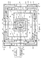
- the prior art coil 10 of Fig. 1 includes two spiral-like, electrically parallel copper windings 12 and 14, each having plural spiral-like turns substantially symmetrically arranged with respect to coil center point 16.
- Windings 12 and 14 are coplanar and have copper conductors with square cross-sections (with each side having a length of about 1.25 cm), including bottom edges spaced approximately 3 cms above the upper faces of the four rectangular quartz windows 21, 22, 23 and 24, individually supported by one-piece, rigid frame 26, made of a non-magnetic metal, preferably anodized aluminum.
- Frame 26 is preferably constructed in a manner similar to that illustrated and described in the '737 patent, except that interior mutually perpendicular rails 28 and 30 are substantially coplanar with the top coplanar faces of windows 21-24.
- Coil 10 is suspended by dielectric hangers from the ceiling of a nonferrous metal (preferably anodized aluminum) electromagnetic shield cover of the type disclosed in Barnes et al. '737.
- Windings 12 and 14 respectively include interior terminals 32 and 34, equispaced from coil center point 16 along rail 28. Terminals 32 and 34 are electrically driven in parallel and connected by metal strap 35 and cable 36 to output terminal 38 of matching network 40, having an input terminal connected to be responsive to RF source 42.
- strap 35 has an inverted U shape with a first leg of the U being spaced substantially farther from windows 21 and 24 than windings 12 and 14, and the other legs running between the first leg and terminals 32 and 34; strap 35 is shown offset to simplify the drawing.
- Windings 12 and 14 also respectively include, at diametrically opposed corners thereof, terminals 44 and 46, respectively connected to ground through capacitors 48 and 50.
- Output terminal 52 of matching network 40 is also grounded to provide a return current path through capacitors 48 and 50 to the matching network grounded terminal for the parallel currents flowing through windings 12 and 14.
- Windings 12 and 14 have a geometry and the values of capacitors 48 and 50 are selected so maximum standing wave currents occur along the lengths of windings 12 and 14 at positions that are somewhat electrically close to terminals 44 and 46.
- the maximum standing wave currents occur in the outermost turn of each of windings 12 and 14 in proximity to rail 26.
- the standing wave current is maximized close to the periphery of coil 10 to increase the magnetic flux density at the periphery of the coil and thereby increase the plasma flux density adjacent the workpiece periphery.
- Each of windings 12 and 14 has a spiral-like configuration and is long enough that transmission line effects occur therein at the frequency of source 42, as described in the previously mentioned co-pending applications.
- the configuration of each of the windings 12 and 14 is frequently referred to as a "square or rectangular" spiral.
- Each of windings 12 and 14 includes 2.125 turns, formed by nine straight segments.
- Each winding includes four straight metal conducting segments extending parallel to rail 28 and five straight metal conducting segments extending parallel to rail 30, whereby each straight line segment intersects its abutting segment approximately at a right angle.
- Terminals 32 and 44 of coil 12 are on one side of rail 30 while terminals 34 and 46 of coil 14 are on the opposite side of rail 30.
- the pitches of the turns of windings 12 and 14 are substantially the same throughout the lengths of the coils between terminals 32, 34 and 44, 46.
- the coil of Fig. 1 can be thought of as having center, intermediate and peripheral portions respectively including approximately two, one and two turns.
- the turns of the center portion include straight metal conducting segments 61-64 of winding 12, as well as straight metal conducting segments 71-74 of winding 14.
- the one turn of the intermediate portion includes straight segments 75 and 76 of winding 12 as well as straight segments 77 and 78 of winding 14.
- the turns of the peripheral portion include straight segments 81-83 of winding 12 as well as straight segments 84-86 of winding 14.
- the coil illustrated in Fig. 1 has previously been used to excite a plasma for etching rectangular, dielectric flat panel display workpieces having straight, rectangular peripheral sides of 550 x 650 mm and 600 x 720 mm. Such workpieces were fixedly located on an electrostatic chuck so the top face of the substrate was approximately 10 cms from the bottom, interior face of windows 21-24.
- the rectangular periphery of coil 10 in this prior art arrangement was somewhat greater than the periphery of the rectangular workpiece; in one prior art configuration, coil 10 was dimensioned so the peripheral, straight mutually perpendicular edges thereof were approximately 650 x 750 mm in dimension so the coil extended to the periphery of the rectangular area defined by windows 21-24 and beyond the rectangular periphery of the workpiece.
- the plasma flux density on the flat panel display workpieces resulting from the coil illustrated in Fig. 1 has a tendency to be relatively low in center and peripheral portions of the workpiece exposed planar rectangular face and to be relatively large in intermediate portions of the workpiece, between the center and peripheral portions thereof.
- the plasma flux density on the workpiece has a tendency to be greatest below the coil intermediate portion, i . e. , below the second half of the first turn and the first half of the second turn of each of windings 12 and 14 and to be lowest below the center and peripheral portions of coil 10.
- the decrease in the plasma flux density at the corners of the peripheral regions of the rectangular workpiece is due to a large extent to the tendency of the plasma resulting from the excitation by coil 10 to have a circular periphery.
- the tendency of the plasma generation region to have a circular periphery results in the plasma flux density in the peripheral regions of the workpiece directly below the peripheral coil portions removed from the coil corners to be substantially greater than the plasma flux density in the peripheral corner regions of the workpiece.
- the plasma flux density profile along a diagonal of the treated workpiece face deviates approximately 21% from complete uniformity.
- the relatively low plasma flux density on the substrate surface portions beneath the center and peripheral portions of coil 10 occurs because the plasma flux has a tendency to diffuse from the center of the plasma toward the intermediate portion of the plasma.
- the coil metal shield structure associated with the vacuum plasma processing chamber has a tendency to cause the magnetic flux derived from coil 10, Fig. 1 , to move away from the chamber periphery toward the center of the chamber, as disclosed in the co-pending, commonly assigned application US 5 800 619 .
- EP-A-0,759,632 discloses a vacuum plasma processor having a vacuum chamber arranged for receiving a gas and having a coil for exciting the gas so as to generate a plasma and wherein the coil has inner and outer portions.
- Another object of the invention is to provide a new and improved vacuum plasma processor having a coil particularly designed so the magnetic flux density derived from it is such that the plasma flux density on a relatively large rectangular workpiece, such as a flat panel display, is relatively uniform, to obviate the tendency for the plasma flux density to be relatively low over center and peripheral regions of the workpiece.
- a further object of the invention is to provide a new and improved coil for a vacuum plasma processor, wherein the coil is particularly designed for providing a relatively uniform plasma flux density on the surface of a relatively large workpiece, particularly workpieces having a rectangular periphery.
- a vacuum plasma processor for treating a workpiece with a plasma comprising a vacuum chamber where the workpiece is adapted to be located, the chamber having an inlet for introducing into the chamber a gas which can be converted into the plasma for treating the workpiece, a coil positioned to couple an RF field to the gas for exciting the gas to the plasma state, the coil including interior, intermediate and peripheral portions, the interior and peripheral portions having turns connected to each other via the intermediate portion, the interior, intermediate and peripheral portions being arranged so the magnetic flux density coupled to the plasma by each of the interior and peripheral coil portions exceeds the magnetic flux density coupled to the plasma by the intermediate coil portion, the coil being arranged so the current density in the coil is substantially greater in the center and peripheral coil portions than in the intermediate coil portion, the coil and workpiece peripheries having similar peripheral dimensions and geometries, characterized by the coil center portion having turns with a tighter pitch than turns in the coil peripheral portion.
- the coil periphery consists of plural straight conductor segments defining a rectangle similar in size and shape to the rectangular workpiece to assist in providing uniform plasma flux density on the rectangular workpiece. At least some, and preferably all, turns of the coil include plural straight segments.
- the coil is preferably arranged so the current density therein is substantially greater in the center and peripheral coil portions than in the intermediate coil portions.
- the coil preferably has a greater number of turns in its center and peripheral portions than in its intermediate portion and the coil center portion has turns with a tighter pitch than turns in the coil peripheral portion.
- the coil includes plural windings electrically connected in parallel so current flows in parallel through terminals of the windings between output terminals of a matching network.
- the plural windings are preferably spatially and electrically substantially symmetrical about a center point of the coil.
- Each of the windings includes plural turns extending radially and circumferentially between the interior and exterior terminals, similar to a spiral.
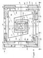
- Fig. 2 of the drawing wherein the prior art coil of Fig. 1 . is modified to include (1) an intermediate portion for coupling a substantially lower magnetic flux density to the intermediate portion of the plasma flux incident on the workpiece relative to center and peripheral portions of the coil and (2) a peripheral portion having additional metal conducting segments for adding magnetic flux to the plasma.
- the added magnetic flux supplements magnetic flux supplied to the plasma by a main part of the coil, i.e., the part of the coil not including the additional segments, to increase the magnetic flux density in the plasma peripheral portions, whereby the magnetic plasma flux density at a rectangular workpiece exposed face becomes more uniform.
- the additional segments are connected in parallel with the main part of the coil.
- Coil 100 of Fig. 2 has a rectangular periphery that is similar in shape and slightly larger in size than the workpiece; the processor of the figures processes rectangular workpieces, preferably cross flat panel displays.
- Coil 100 includes two electrically parallel windings 102 and 104, electrically connected to ungrounded and grounded output terminals 38 and 52 of matching network 40, in turn responsive to 13.56 MHz RF source 42.
- Windings 102 and 104 have a common central terminal 106, coincident with coil center point 16, about which all of coil 100 is substantially diagonally (and therefore diametrically) symmetrical.
- Terminal 106 is connected by an electrically conductive strap (not shown) to matching terminal output terminal 38.
- Windings 102 and 104 include diagonally opposed peripheral terminals 108 and 109, at opposite peripheral corners of coil 100.
- Terminals 108 and 109 are respectively connected to grounded terminal 52 of matching network 40 via capacitors 48 and 50.
- Each of windings 102 and 104 has an electrical length for the frequency of source 42 such that transmission line effects occur in the windings.
- the lengths of windings 102 and 104 and the frequency of source 42 are usually such that the distance along each winding is slightly less than a half wavelength of the source frequency.
- the values of capacitors 48 and 50 are selected so peak and minimum standing wave currents respectively occur in the peripheral and interior portions of the windings.
- the peak standing wave currents occur approximately at the point of the outermost turns of windings 102 and 104 which are approximately aligned with rail 30 that support windows 21-24 and the minimum standing wave currents are approximately at terminal 106, where the standing wave voltage has a peak value. Because the maximum standing wave current occurs about 3/8 of a turn from each of terminals 108 and 109, relatively large magnetic flux densities are imparted by the main peripheral part of coil 100 to the peripheral portion of the plasma incident on the peripheral portion of the workpiece.
- Coil 110 includes (1) a three turn central portion 112 (including straight metal conducting segments 113-124, extending radially and circumferentially from center terminal 106 to which they are electrically connected by metal struts 111 and 112), (2) approximately one turn intermediate portion 130 (including straight radially and circumferentially extending metal conducting segments 131-134), and (3) approximately two turn peripheral portion 140 (including straight radially and circumferentially extending metal conducting segments 141-146).
- the turns of peripheral portion 140 have a substantially greater pitch than the single turn 132 of intermediate portion 130, which in turn has a pitch considerably greater than the tightly pitched turns of center portion 110.
- Intermediate portion 130 is substantially radially displaced from center portion 110, but is somewhat radially close to peripheral portion 140.
- Each of the coplanar straight metal conducting segments 113-124, 131-134 and 141-146 of portions 110, 130, 140 is preferably formed of copper having a square cross-section of approximately 1.25 cm on each edge and is spaced so its bottom edge is approximately 3 cms above the top faces of windows 21-24, having bottom faces about 10 cms above the planar processed workpiece surface.
- the windings of coil 100 are suspended by dielectric hangers from the ceiling of a non-ferrous metal (preferably anodized aluminum) coil shielding cover of a type disclosed in the Barnes et al. patent.
- the exterior ends of center coil portion 110 are electrically connected by metal, preferably copper, struts 150 and 152 to the interior ends of intermediate coil portion 120.
- the struts have an inverted U shape, with a first leg lying in a plane appreciably above the plane of the straight conducting segments of portions 110, 130 and 140 and two downwardly depending legs electrically and mechanically connecting the first leg to coil 100.
- the struts have a 0.3 x 2.5 cm cross section with the 2.5 cm edge being parallel to windows 21-24.
- the coil of Fig. 2 is designed so there is a greater current density in the center and peripheral coil portions 110 and 140 than in intermediate coil portion 130. Thereby the magnetic flux densities derived from the center and peripheral coil portions are greater than the magnetic flux density derived from the intermediate coil portion. Consequently, the tendency of the plasma flux density incident on the workpiece in the vacuum chamber to be greater in the intermediate portions of the workpiece than in the center and peripheral portions of the workpiece is reduced.
- the plasma flux density in the center portion of the prior art processor including the coil of Fig. 1 has a tendency to be relatively low because the plasma has a tendency to diffuse away from the center portion of the plasma.
- the tendency in the prior art of the plasma flux density to be relatively low in the peripheral portions of the plasma occurs because the plasma generated by the prior art coil has a maximum plasma flux density in a ring-shaped region at some intermediate distance between the center and the periphery of the coil.
- the distance between the top of the workpiece and the underside of the dielectric windows must be sufficiently large as to allow for plasma diffusion.
- the plasma diffusion causes the ring-shaped region to average out into a more uniform plasma flux density at the workpiece.
- the coil of Fig. 2 improves the plasma flux density over the prior art by supplying (1) more magnetic flux density to the center plasma portions than to the intermediate plasma portions and (2) additional magnetic flux density to the periphery of the plasma to at least partially overcome the effects of the shielding structure.
- the improved results occur because, inter alia, the center and peripheral portions 110 and 140 of coil 100 have a greater number of turns than intermediate portion 130.
- the turn of intermediate portion 130 is spaced from the exterior turn of center portion 110 such that the diameter of the intermediate portion turn is approximately twice the outer diameter of the center portion exterior turn.
- the single turn of intermediate portion 130 circumscribes an area which is approximately four times the area circumscribed by the three turns of center portion 110 and the single turn of the intermediate portion is spaced from center point 16 by twice the distance that the exterior turn of center portion 110 is spaced from the coil central point.
- the single turn of intermediate portion 130 is spaced from the turns of peripheral portion 140 by about the same distance that the turns of the peripheral portion are spaced from each other in the coil of Fig. 2 .
- straight conductor segments 131-134 are spaced from straight conductor segments 141-145 by approximately the same distance that straight conductor segments 141 and 144 are spaced from straight conductor segments 146 and 143, respectively.
- center coil portion 110 and its somewhat remote spacing from intermediate coil portion 130 help to overcome the tendency for a relatively low plasma flux density to be incident on the center of the workpiece.
- the tight pitch of center coil portion 110 and its separation from the rest of coil 100 cause close self coupling of the magnetic flux derived from the center coil portion to concentrate the magnetic flux (i.e. increase the magnetic flux density) derived from center portion 10.
- peripheral coil portion 140 is modified relative to the prior art coil of Fig. 1 .
- the main portion of the coil of Fig. 2 (consisting of conductor segments 113-128, 131-134 and 141-146, as well as struts 111, 112, 150 and 152) has additional structure added to its periphery to increase the magnetic flux density in the periphery of the plasma, particularly the parts of the plasma close to corners of the rectangular processing chamber.
- peripheral coil portion 140 includes additional electrically conducting winding segments 161-168, spatially adjacent to the four peripheral corners of the coil peripheral terminals 108 and 109.
- the odd numbered ones of winding segments 161-168 are part of and added to winding 102, while the even numbered ones of winding segments 161-168 are part of and added to winding 104.
- Winding segments 161-168 are co-planar with conductor segments 113-124, 131-134 and 141-146 and cause additional RF current to flow in the peripheral portions of coil 100, particularly at the corners of the coil where the magnetic and plasma flux densities have a tendency to be otherwise relatively low.
- the RF current flowing in winding segments 161-168 adds magnetic flux to the corners of the plasma processing chamber.
- the magnetic flux added by segments 161-168 to the processing chamber aids the magnetic flux supplied to the processing chamber by conductor segments 141-146 of the main coil portion to increase the plasma flux density below the corners of the coil and overcome to a large extent the non-uniformity of the plasma flux density at the corners of the rectangular workpiece and vacuum chamber.
- the magnetic fluxes established by the straight intersecting conductor segments 141-146 (which form 90° corners) have longitudinal axes substantially at right angles to each other and bend around the corners of the coil, vacuum chamber and workpiece; the magnetic fluxes established by segments 161-168 have axes extending generally in the same direction as the straight segments 141-146 with which they are spatially adjacent and electrically connected in parallel.
- each of added, diagonally opposed coil segments 161 and 162 includes four straight, mutually perpendicular copper conductor segments 182-185.
- Conductor segments 184 and 185 of coil segment 161 respectively extend parallel to and are positioned outwardly from (by the same distances) straight segments 132 and 141, with segment 184 extending from the corner intersection of segments 132 and 141 by a smaller distance than segment 185.
- Segments 184 and 185 are respectively connected to segments 132 and 141 by stub segments 182 and 183.
- Segment 162 has a geometry identical to that of segment 161, but is at the corner defined by intersecting straight line segments 134 and 144.
- Winding segment 163 includes two electrically and spatially parallel conductor segments 187 and 188, respectively positioned outwardly and inwardly of and extending parallel to conductor segment 142.
- Segment 187 is connected in series with conductor segment 189 that is positioned outside and extends parallel to conductor segment 141; segments 187 and 189 have about the same length that is somewhat greater than the length of segment 188. Electrical parallel connections from main coil conductor segments 141 and 142 to parallel conductor segments 187-189 are established by stub conductor segments 191-193, extending at right angles to the conductor segments 141, 142 and 187-189 with which they are physically connected. Corner winding segment 164, constructed identically to corner winding segment 163, is diametrically opposite from segment 163 and intersects straight conductor segments 144 and 145 at the corner formed by them.
- Each of additional diagonally opposed winding segments 165 and 166 respectively at and electrically connected in parallel with the corners defined by the intersection of conductor segments 142 and 143 and the intersection defined by conductor segments 145 and 146, includes conductor segments 198, 200, 204 and 206. Segments 198, 200, 202 and 204 provide parallel current paths slightly outside the corners associated with them. The end of conductor segment 198 remote from the corner is closer to center rail 30 than is the corresponding conductor segment 183 of winding segment 162, to further increase the magnetic flux density close to the wall of the vacuum plasma processing chamber.
- Winding segments 167 and 168 respectively at and electrically connected in parallel with the diagonally opposed peripheral corners where end terminals 109 and 108 are located, respectively include elongated conductor segments 208 and 209 that extend parallel to and are slightly outside of conductor segments 143 and 146. Segments 208 and 209 are respectively connected by stub straight conductor segments 212 and 213 to conductor segments 143 and 146. The magnetic fluxes of segments 167 and 168 aid the magnetic fluxes of segments 143 and 146 to increase the peripheral plasma flux density.
- each of the outer conductors of additional peripheral winding segments 163-168 i.e. conductors 187, 187', 200, 200', 202, 202', 208 and 209, are set back slightly from the outer edges of windows 21-24 so the magnetic flux derived by these conductors is effectively added to the plasma.
- corresponding parts of opposite peripheral winding segments bear the same reference numerals except that primes are added to the peripheral winding segments that are not specifically described.
- the magnetic flux resulting from the current flowing through segments 161-168 is added to the magnetic flux resulting from the current flowing in the main part of the coil.
- the additional magnetic flux increases the magnetic flux at the periphery of the vacuum plasma processing chamber, particularly in the corners of the chamber, to increase the plasma flux density in the peripheral portions of the workpiece so the plasma flux density incident on the workpiece is more uniform than the prior art of Fig. 1 .
- Struts 220 and 222 have the same dimensions and geometrical orientation as struts 150 and 152, being shaped as inverted U's. Thereby, a negligible amount of magnetic flux is added to the plasma by struts 220 and 222.
- Conducting segments 224 and 226 extend parallel to rail 30, inwardly from conducting segments 132 and 134, respectively.
- the length of each of conducting segments 224 and 226 is less than one half the spacing of conducting segments 132 and 134 from rail 28. Thereby, the end of each of conducting segments 224 and 226 remote from conducting segments 132 and 134 is substantially outside the exterior turn of internal coil portion 110.
- Struts 220 and 222 extend from the end terminals of the interior coil portion 110 to the ends of coil portions 224 and 226 remote from coil segments 132 and 134, respectively.
- the coil of Fig. 3 is modified to (1) eliminate conductor portions 224 and 226 and (2) locate the additional peripheral parallel coil segments 161-168 so they are closer to the plasma than the remaining conducting coil segments.
- intermediate coil portion 130 is modified to include only approximately one half of conductors 132 and 134, i.e., coil portion 130 includes only the part of conductor 132 to the right of rail 30 and the part of conductor 134 to the left of rail 30 (as viewed in Fig. 4 ).
- conducting portions 224 and 226 of Fig. 3 are completely eliminated and the ends of conductors 132 and 134 are electrically connected to end terminals of center coil portion 110 by metal inverted U shaped struts 230 and 232.
- Struts 230 and 232 are very similar to struts 220 and 222, except struts 230 and 232 are connected directly to the ends of conductor segments 132 and 134 of coil center portion 110. Consequently, the magnetic flux density in the intermediate part of the plasma is lower for the coil of Fig. 4 than for the coils of Figs. 1-3 .
- parallel peripheral segments 161-168 are not coplanar with the conducting segments 113-124, 132, 134 and 141-146 of the main part of the coil. Instead, the parts of the parallel peripheral segments that supply the greatest amount of magnetic flux to the plasma are closer to the plasma as a result of these parallel peripheral coil segments being much closer to the top face of windows 21-24 than are the conducting segments of the main part of the coil.
- Each of parallel peripheral segments 161-168 of the coil of Fig. 4 includes a straight conducting segment that is close to the plane of windows 21-24.
- the conducting segments in different planes are mechanically and electrically connected to each other by metal straps having cross sectional dimensions similar to struts 230 and 232. As illustrated in Figs. 4A and 4B , the metal straps extend downwardly from the conductor segments in the main plane of the coil, thence horizontally to the conductor segments of parallel segments 161-168.
- conducting segments close to windows 21-24 are mechanically and electrically connected, as appropriate, to conducting segments 141-146 by metal straps 182, 183, 182', 183', 191, 192, 193, 191', 192', 193', 198, 204, 198', 204', 206, 207, 206', 207', 212, 213, 212' and 213' that extend parallel to and at right angles to the plane of windows 21-24.
- conducting segments 184, 185, 184', 185', 187, 188, 189, 187', 188', 189', 200, 202, 200', 202', 208 and 209 close to windows 21-24 are adjacent to the periphery of the plasma, these conducting segments couple greater RF excitation power to the plasma corners than is achieved with the coplanar parallel peripheral segments of Figs. 2 and 3 .
- the increased RF excitation occurs because of the increased magnetic field density resulting from the closer proximity of the conducting segments close to windows 21-24 than the coplanar parallel peripheral conducting segments of Figs. 2 and 3 .
- Fig. 5 including plots of silicon etch rate in Angstroms per minute from flat circular workpieces, each having an exposed surface uniformly coated with silicon; the workpieces were laid out along a diagonal of a plasma processing chamber having a rectangular shape, as described infra in connection with Figs. 6-8 . Since etch rate is directly dependent on plasma flux density the measurements of etch rate are directly correlated with plasma flux density. The etch rate is plotted for (1) the prior art coil of Fig. 1 (plot 260), (2) a coil having center, intermediate and peripheral portions as illustrated in Fig. 1 , in combination with the peripheral parallel coil segments of Fig. 2 (plot 262), (3) the coil of Fig.
- Plots 260-266 were obtained from plasma processing chambers operating under the same conditions, to the extent possible and practical. Etch rate is indicated along the Y axis in Fig. 5 , while distance along the diagonal of the workpiece surface is indicated in the X axis direction. The workpiece center and peripheral corner along the diagonal are respectively indicated by the numerics "2" and "15" in the X axis direction.
- the measurements presented in Fig. 5 indicate the plasma flux densities deviate from uniformity for the coils associated with plots 260, 262, 264, 266 and 268 by 21.5%, 18.9%, 17.9%, 14.7% and 13.0%, respectively.
- Fig. 5 provides some interesting data about plasma flux density as a function of workpiece radial position.
- a minimal etch rate of approximately 1,825 Angstroms per minute occurs at the center of the workpiece.
- the minimum values occur at point 3 along the X axis, i.e., at a point displaced from the workpiece center.
- the lack of symmetry indicated by plots 262-268 probably occurs because the magnetic flux densities derived from the coils of Figs. 2-4 are not completely symmetrical as a result of added conductor segments 188 and 188'.
- the minimum value of plasma flux density in the workpiece center, indicated by plot 268, is substantially higher than the center etch rates of any of plots 262-266.
- the greater magnetic flux isolation provided by the structure of Fig. 4 for center coil portion 110 relative to intermediate and peripheral coil portions 130 and 140 causes a substantial increase in the magnetic flux in the center of the plasma. Greater magnetic flux isolation occurs in the coil of Fig. 4 than in the coils of Figs. 2 and 3 because (1) the conducting segments of intermediate portion 130 are shorter in Fig. 4 than in Figs.
- peripheral portion 140 a significant part of peripheral portion 140 (viz: the conducting segments 184, 185, 184', 185', 187, 188, 189, 187', 188', 189', 200, 202, 200', 202', 208 and 209) is farther from portion 110 in Fig. 4 than in Figs. 2 and 3 .
- Moving the additional parallel conducting segments from the plane of the main coil close to the upper faces of windows 21-24 causes an appreciable increase in the peripheral etch rate.
- etch rates in the intermediate part of the workpiece, between numerics 6 and 12 in the X axis direction of Fig. 5 are virtually the same for the coils of Figs. 3 and 4 , as indicated by plots 266 and 268.
- the etch rates indicated by plots 266 and 268 are substantially higher in the intermediate portion of the workpiece than are the etch rates for the coil of Fig. 2 (plot 264) and the unillustrated coil indicated by plot 262.
- Figs. 5A and 5B are plots of silicon etch rate, in Angstroms per minute, under identical conditions, as far as practical, of two glass 600 x 720 mm flat panel display substrates uniformly coated with silicon in vacuum chambers respectively including the coils of Figs. 1 and 4 .
- the etch rates were measured at equally spaced matrix points on the panel; measurements adjacent the panel edges were made 15 mm from these edges.
- the decrease in average etch rate is attributed to more equal loading by the plasma of the coil of Fig. 4 than by the plasma of the coil of Fig. 1 .
- the etch rates of 1989, 1904, 2071, 2023, 2033, 2028, 2031, 1899, 1831, 1909, 2065 and 2000 resulting from the Fig. 1 coil are materially respectively reduced to 1700, 1629, 1595, 1578, 1755, 1668, 1765, 1710, 1712, 1645, 1724 and 1611 when the Fig. 4 coil was used.
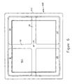
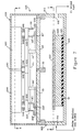
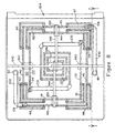
- Figs. 6 , 7 and 8 of the drawing wherein the coil of Fig. 4 is illustrated as being included in a vacuum processor 600 including vacuum chamber 602 and electromagnetic shield cover 604, preferably formed of anodized aluminum.
- the exterior of vacuum chamber 602 is defined by windows 21-24, rails 28 and 30, anodized, aluminum sidewalls 610, and anodized aluminum floor 614.
- Sidewalls 610 include ports 616 and 618, respectively connected to an ionizable gas source and a vacuum pump (neither shown).
- the vacuum pump establishes appropriate vacuum conditions in chamber 602, enabling the ionizable gas flowing through port 616 to be excited by the electromagnetic field derived by the coil of Fig. 4 to be excited to a plasma state.
- Chamber 602 and cover 604 are mechanically and electrically connected to each other and to ground potential by appropriate contacts and provide a shield to confine the magnetic and electric fields derived by the coil.
- the shield reduces the RF field density derived from the coil so the magnetic and electric fields close to the shield are considerably lower than the fields toward the center of the plasma processor.
- electrostatic chuck 620 which holds workpiece 622 in situ while the workpiece is being processed; in one preferred use of the processor, substrate 622 is a rectangular glass substrate for an electrostatic display panel. Electrostatic chuck 620 is electrically isolated from the ground potential of metal cover 604, walls 610 and floor 614 by electric insulating sheet 624. DC voltage from a suitable source (not shown) is applied as a clamping potential to electrostatic chuck 620, which is also connected via a matching network to an RF source (not shown) that RF biases the electrostatic chuck and workpiece 622. In addition, the back face of workpiece 622 is preferably cooled by providing grooves in chuck 620.
- ionizable gas is introduced into the interior of vacuum chamber 602 by a plenum or manifold mounted on windows 21-24; to simplify the presentation, such a plenum or manifold is not illustrated, as such structures are well known to those skilled in the art.
- Chamber 602 and cover 604 are constructed such that processor 600 is configured as a right parallelepiped to accommodate rectangular glass flat panel display workpiece 622. It is to be understood, however, that the periphery of processor 600 is modified so the periphery of the processor is similar in size and shape to the workpiece periphery if the workpiece has other peripheral configurations.
- the periphery of substrate 622 is slightly smaller than the periphery of the coil of Fig. 4 , which is in turn slightly smaller than the combined periphery of windows 21-24.
- the efficiency of generating sufficient plasma flux at the large area workpiece is improved over the prior art of Fig. 1 , to enable the power requirements of the RF sources energizing the coil of Fig. 4 and the biasing chuck 620 to be maintained at a relatively low level; in one embodiment, RF source 42 has an output power of 5 kW.
- capacitors 48 and 50 are mounted in the volume between the upper face of windows 21-24 and the top of cover 604 so the circular cross-sections thereof are parallel to the windows.
- Capacitors 48 and 50 are connected to output terminals 108 and 109 of the coil of Fig. 4 by copper struts 630 and 632, both of which extend parallel to rail 28, in a plane parallel to the upper faces of windows 21-24.
- the coil of Fig. 4 is supported by a structure including electrical insulating, elongated bars 640, 642 and 644, suspended from the ceiling of cover 604.
- the main portion of the coil of Fig. 4 is mechanically connected to bars 640, 642 and 644 by electrical insulating vertically extending support posts 648, in turn mechanically connected to horizontally extending electrical insulating coil support plates 648 and 650. Plates 650 support peripheral portion 140 of the coil, and center coil portion 110 is supported by center post 646.
- the bottom faces of the peripheral, corner segments of the coil are slightly spaced from the top faces of windows 21-24; in Fig. 7 , coil segments 189 and 209 are illustrated as being proximate the upper face of window 21 and are connected to coil segments 141 and 146 by curved struts 193 and 206', respectively. Coil segments 141 and 146 are in turn illustrated as being suspended from the bottom face of coil support face 650.
- the bottom faces of segments 189 and 209 are vertically spaced from the top face of window 21 by approximately 0.56 cm and the bottom faces of main coil segments 141 and 192 are vertically spaced by about 2.2 cm from the bottom faces of peripheral coil segments 189 and 209.
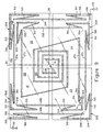
- FIG. 9 A bottom view of a further coil in accordance with the present invention is illustrated in Fig. 9 .
- the main part of the coil which is similar in certain respects to the main parts of the coils of the embodiments of Fig. 2-4 , has added to it peripheral segments that are connected in series with corners in the peripheral portions of the main part of the coil.
- the corners are formed by conducting segments that extend substantially at right angles to each other, having non-contacting adjacent ends that almost meet.
- the additional series conductor segments in the peripheral portion of the coil have current flowing in them in the same spatial direction as the spatially adjacent conducting elements so that the magnetic flux coupled by these additional conducting segments to the plasma is additive to the magnetic flux derived from the main part of the coil.
- the coil of Fig. 9 includes center and intermediate portions 110 and 130 which are identical with the corresponding center and intermediate portions of the coil of Fig. 4 .
- the peripheral portion 140 of the coil illustrated in Fig. 8 is, however, quite different from the coils of the embodiments of Fig. 2-4 .
- the main part of the peripheral portion 140 includes straight conducting segments 270, 272, 274 and 276, each of which is parallel to rail 28, as well as straight conducting segments 280, 282, 284 and 286, each of which is parallel to rail 30.
- straight conducting segments 270-276 and 280-286 are in direct contact. Instead, there is a gap at each of the four interior corners 291-294 and the two exterior corners 295 and 296 formed by a pair of adjacent ones of segments 270-276 and 280-286.
- a pair of supplemental, mutually perpendicular straight segments is connected to the non-abutting ends of coil segments 270-276 and 280-286.
- the supplemental coil segments supply additional magnetic flux to the plasma periphery.
- the additional series-connected segments are illustrated in Fig. 9 as being co-planar with the straight segments of center and intermediate coil portions 110 and 130, as well as straight segments 260-276 and 280-286 of the peripheral portion of the main coil part.
- the supplemental portions can be closer to the plasma than the remainder of the coil; in such an instance, the supplemental straight conductors would be slightly above the upper faces of windows 21-24, considerably closer to the windows than main coil part conducting segments 270-276 and 280-286.
- the supplemental conducting segments are connected to these ends of the conducting segments of the main peripheral part of the coil by metal electrically conducting struts 310, having the same dimensional and positional attributes as discussed supra for the conducting struts of Figs. 2-4 .
- corners 291-296 where straight conductor segments 270, 272, 274, 276, 280, 282, 284 and 286 almost, but do not quite, intersect are respectively connected to additional conductor segments 301-306 by diagonally extending metal struts 310.
- Each of additional conducting segments 301-306 includes two straight intersecting conducting elements 312 and 314, respectively extending parallel to rails 28 and 30.
- Conducting elements 312 and 314 of each of supplemental conducting portions 301-306 intersect at a point substantially aligned with the "corner" in the gap defined by the projection of the mutually orthogonal straight conductor segments of the main part of the coil next to a particular additional segment.
- Conducting elements 312 and 314 are spatially close to the conducting segments of the main part of the coil and are electrically connected in series with these straight conducting segments of the main part of the coil.
- the spatial arrangement of conductors 312 and 314 and of the straight conducting segments of the main coil part is such that the currents in elements 312 and 314 flow in the same direction as the currents which flow in the portions of conducting segments 270, 272, 274, 276, 280, 282, 284 and 286 with which the particular pair of conducting elements 312 and 314 is adjacent.
- magnetic fluxes resulting from the currents flowing in conducting elements 312 and 314 and conducting segments 270-276 and 280-286 are additive in the peripheral parts of the plasma, to increase the plasma flux density in the plasma periphery relative to the prior art of Fig. 1 .
- conducting elements 312 and 314 are coplanar with the conducting segments of the main part of the coil; however, it is to be understood that elements 312 and 314 can be positioned so they almost abut the faces of windows 21-24, i.e., are closer to the plasma than the conducting segments of the main part of the coil.
- the coil of Fig. 9 has additional series, straight, metal conducting elements 316 and 318 (extending parallel to rail 30) that are connected between the main part of the coil and output terminals 108 and 109 by struts 319, that are identical to struts 310. Opposite ends of element 316 are connected to terminal 108 directly and to an end of conductor 284 adjacent additional corner segment 304 by one of struts 319, while opposite ends of element 318 are connected to terminal 109 directly and to an end of conductor 286 adjacent additional corner segment 304 by the other one of struts 319.
- Struts 319 have an inverted U shape, arranged so the legs thereof extending parallel to faces 21 and 24 are substantially farther from the plasma than the conducting segments in the main part of the coil.
- the magnetic fluxes from element 316 and conductor 284 add at the coil corner adjacent terminal 108 and the magnetic fluxes from element 318 and conductor 286 add at the coil corner adjacent terminal 109. There are negligible magnetic flux bucking effects resulting from currents flowing in struts 309.
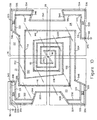
- Fig. 10 of the drawing another modification of the coil illustrated in Fig. 4 .
- the magnetic flux density and plasma flux density in the peripheral corners of the plasma are substantially increased relative to the prior art of Fig. 1 by modifying the peripheral portion of the coil to include supplemental conductor segments 321-324, one of which is at each of the four peripheral corners of the coil.
- Each of supplemental peripheral corner coil segments 321-324 includes four straight conductor elements 331-334, arranged so elements 331 and 333 extend parallel to rail 28, while elements 332 and 334 extend parallel to rail 30.
- Elements 331 and 333 intersect in the peripheral part of the coil at corner 335, while elements 333 and 334 intersect at the peripheral corners of the coil at corner 336.
- Elements 331 and 332 thus form a first leg which is inside of and nested with a second leg formed by elements 333 and 334. Ends of straight conducting elements 331 and 333 of corner segments 321 and 324 remote from corners 335 and 336 are connected to each other by straight conducting element 338, extending parallel to rail 30.
- Terminals 340 and 342 of the coil illustrated in Fig. 10 are at the corners defined by the intersections of elements 333 and 338 of corner segments 321 and 324, respectively.
- Terminals 340 and 342 are connected to the ground or output terminal of the matching network (not shown in Fig. 10 ) by series connections established through capacitors 48 and 50, respectively.
- the peripheral terminals of the coil illustrated in Fig. 10 are displaced from the corners of the coil, in contrast to the coil configurations of each of Figs. 1-4 and 9 .
- Corner segments 321 and 324 are thus respectively electrically in series with the coil output terminals 340 and 342 and the remainder of the coil.
- the series connections are established through metal struts 344, each of which extends diagonally outwardly from the main part of the coil and is electrically connected to the ends of elements 332 and 334 remote from corners 335 and 336, to assist in establishing the parallel current paths of corner segments 321 and 324.
- Elements 331 and 332 have approximately the same length, which is somewhat shorter than the equal lengths of elements 333 and 334.
- Corner segments 322 and 323 differ somewhat from corner segments 321 and 324 because there are no terminals at corner segments 322 and 323. Corner segments 322 and 323 are electrically connected to the remainder of the coil by diagonally and outwardly extending metal struts 346 and 348; strut 346 is connected to the ends of conductor elements 331 and 333 (of corner segments 322 and 323) which are remote from corners 335 and 336. Similarly, metal struts 348 are electrically connected to the ends of conductor elements 332 and 334 of corner segments 322 and 323, which element ends are remote from corners 335 and 336, respectively.
- segments 350 are removed from the outer periphery of the coil illustrated in Fig. 10 , but are positioned sufficiently close to the peripheries of windows 21-24 to add magnetic flux to the peripheral portion of the plasma and increase the plasma flux density in the peripheral part of the plasma at regions removed from the corners of the plasma and the workpiece.
- the inner ends of conducting struts 346 remote from corner segments 322 and 323 are connected to an end of each of conductor segments 352 and 354, both of which extend parallel to rail 28.
- the other ends of conductor segments 352 and 354 are respectively connected to the ends of conductor segments 141 and 142 remote from conductor segments 130 and 132.
- Conductor segments 352 and 354, in the peripheral portion of the coil, are respectively connected to one end of segments 141 and 144 of the intermediate portion of the coil that also includes conductor segments 132 and 134.
- the ends of conductor segments 132 and 134 are respectively connected to interior coil portion 110 by struts 230 and 232 in the same manner that the intermediate portion of the coil of Fig. 4 is connected to the interior portion 110 thereof.
- Segments 350 are positioned inwardly from the periphery of the coil illustrated in Fig. 10 to provide greater uniformity of the plasma flux density incident on the workpiece than is attained with the prior art coil of Fig. 1 .
- the plasma flux density has a tendency to be lower in the peripheral corners of the chamber than in the peripheral portions of the chamber removed from the corners. To reduce this effect, straight segments 350 are set back from the outer coil periphery.
- Each of metal struts 344, 346 and 348 has four legs, a first of which extends parallel to the faces of windows 21-24 and is positioned substantially farther from windows 21-24 than conductor segments 331-334 of peripheral portions 321-324. The remaining three legs of each of struts 344, 346 and 348 extend vertically between the first leg of the strut and one of conductor segments 331-334, 352 and 354, as appropriate. The construction and positions of struts 344, 346 and 348 minimize the magnetic flux effects of the struts on the plasma.
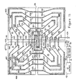
- Fig. 11 of the drawing a bottom view of still a further coil in accordance with the invention.
- a more uniform plasma flux density is generated at workpiece peripheral regions by adding segments to the corner locations of the turns of a pair of parallel windings forming a main coil.
- the added corner segments are connected in series with the remainder of each winding.
- Each winding has short (relative to the short segments of the coils of Figs. 2-4 and 9) straight conducting segments in series between the added segments at a pair of corners in different adjacent quadrants of the coil, i.e., at or close to peripheral corners of adjacent ones of windows 21-24.
- the short straight segments cause a relatively large gap between the corner segments and the straight segments compared to the gaps between the corners and straight segments in the coil of Fig. 9 ; of course there is no gap between the corners and straight segments in the coils of Figs. 1-4 . Additionally, the lengths of the straight segments of the main coil have been substantially reduced to increase the gap between the corners and the short straight segments removed from the corners.
- the coil of Fig. 11 is characterized by complete symmetry and has great flexibility through selective use of different conductor segments thereof.
- the coil of Fig. 11 includes two parallel windings 402 and 404, which together form interior, intermediate and peripheral portions 406, 408 and 410 of the coil.
- Winding 402 includes interior and exterior terminals 412 and 414, while winding 404 includes interior and exterior terminals 416 and 418.
- Interior terminals 412 and 416 are connected to ungrounded output terminal 38 of matching network 40 by cable 420 and U-shaped strut 422 while terminals 414 and 418 are connected by capacitors (i.e. reactive impedances) 424 and 426 to the grounded output terminal of matching network 40.
- capacitors i.e. reactive impedances
- the values of capacitor 424 and 426 and the lengths of windings 402 and 404 relative to the wavelength of source 42 are such that the peak standing wave current occurs approximately in the center of exterior portion 410 of the coil.
- Interior terminals 412 and 416 are positioned along a line extending through center point 428 of the coil, as well as on the center longitudinal axis of rail 28. Exterior terminals 414 and 418 are equispaced from coil center 428 and diagonally located on opposite sides of the longitudinal axis of rail 30.
- Interior coil portion 406 includes straight coil segments 431, 432, 433 and 434 of winding 402, as well as straight coil segments 435, 436, 437 and 438 of winding 404.
- Coil segments 431, 433, 435 and 437 extend parallel to rail 30, while straight coil segments 432, 434, 436 and 438 extend parallel to rail segment 28, with segment 432 intersecting segments 431 and 433, segments 433 and 434 intersecting, segment 436 intersecting segments 435 and 437, and segments 437 and 438 intersecting.
- Peripheral coil portion 410 includes straight conducting segments at corners 441, 442, 443 and 444 of windows 21, 22, 23 and 24, respectively. Since each of the straight conducting segments at each of corners 441-444 is identical, a description of the straight conducting segments 451-458 of only corner 441 is given.
- Straight conducting segments 451-458 form four nested corners, such that conducting segments 451, 453, 455 and 457 extend parallel to rail 28, while conducting segments 452, 454, 456 and 458 extend parallel to rail 30.
- Straight conducting segments 451-458 are arranged in pairs, such that adjacently numbered conducting segments form one pair and have abutting ends at a corner.
- the corners formed by conducting segments 451-458 are aligned along line 460, that intersects coil center point 428.
- Conducting segments 451, 453, 455 and 457 have progressively increasing lengths in the stated order, and conducting segments 452, 454, 456 and 458 have progressively increasing lengths in the stated order.
- segments 451-458 are such that the ends of segments 451, 453, 455 and 457 spaced from line 460 are progressively farther from rail 30, while the ends of segments 454, 456 and 458 spaced from line 460 are equispaced from rail 28, but the end of segment 452 spaced from line 460 is farther from rail 28 than segments 454, 456 and 458.
- the nested arrangement of conductors 451-458 causes a substantial increase in magnetic flux density (relative to the coil of Fig. 1 ) in the plasma peripheral corner below coil corner 441.
- the magnetic flux density derived from each of corners 441-444 is greatest below the exterior region of the coil and decreases toward the center of the coil so the magnetic flux density established by the conducting segments of the corners is somewhat less in the plasma portion below short conducting segments 451, 452 than it is in the plasma portion below long conducting segments 457, 458.
- This variation in magnetic flux density in the plasma has a tendency to make the plasma flux density more uniform in the corners relative to the prior art of Fig. 1 .
- Peripheral coil portion 410 also includes straight, equal length conducting segments 471-476 that extend at right angles to the longitudinal axis of rail 28, such that the ends of conducting segments 471-476 are equispaced from the axis of rail 28; segments 471-473 are on the same side of rail 30 as terminal 30 and segments 474-476 are on the opposite side of rail 30.
- Peripheral coil portion 410 also includes straight, equal length conducting segments 481-486 which extend at right angles to the longitudinal axis of rail 30 and have opposite ends equispaced from the longitudinal axis of rail 30.
- Conducting segments 481-483 are located on the side of coil 400 between center point 428 and terminal 418, while conducting segments 484-486 are located on the opposite side of coil 400, i.e., the side between coil center point 428 and terminal 414.
- Intermediate coil portion 408 includes straight coil segments 491-494, wherein equal length coil segments 491 and 493 are equidistant from coil center point 428 along rail 20 and extend at right angles to the longitudinal axis of rail 28, such that opposite ends of each of coils 491 and 493 are equispaced from the rail 28 longitudinal axis.
- Each of segments 491 and 493 has the same length as coil segments 471-476, whereby the ends of all of straight coil segments 471-476, 491 and 493 are equidistant from the longitudinal axis of rail 28.
- Each of straight coil segments 492 and 494 has the same length as coil segments 481-486 and extends at right angles to the longitudinal axis of rail 30, such that the centers of coil segments 492 and 494 are coincident with the longitudinal axis of rail 30 and are on opposite sides of coil center point 428.
- the conducting segments of winding 402 are interconnected by electric conducting metal struts 501-516, while the conducting segments of winding 404 are connected by electric conducting metal struts 521-536.
- the conducting segments and struts are arranged whereby the interlaced turns of parallel windings 402 and 404 extend radially and circumferentially in a spiral like manner between interior terminals 412 and 416 and exterior terminals 414 and 418.
- Each of struts 501-516 and 521-536 has an inverted U shape and is constructed basically the same as the struts of Figs. 2-4 , 9 and 10 so as not to appreciably affect the RF fields derived from conducting segments 431-438, 451-458, 471-476, 481-486 and 491-494.
- the latter conducting segments are coplanar in the coil illustrated in Fig. 11 but in other coils peripheral conducting segments 455-458 are closer to windows 21-24 than others of the conducting segments.
- each of windings 402 and 404 is less than one-half of a wavelength of the RF excitation frequency derived by RF source 42.
- the values of capacitors 424 and 426 and the lengths of windings 402 and 404 are such that (1) the peak standing wave current occurs in each of windings 402 and 404 in a middle part of peripheral winding portion 410 and (2) the standing wave current at interior terminals 412 and 416 of windings 402 and 404 is relatively low.
- Typical points where the maximum standing wave currents occur in windings 402 and 404 are at the centers of conducting portions 472 and 475.
- the standing wave voltages at interior terminals 412 and 416 are relatively high and decrease to relatively low values at exterior terminals 414 and 418.
- the instantaneous current flow in the conducting segments of windings 402 and 404, other than in struts 501-516 and 521-536, is in the same direction in spatially adjacent conducting segments.
- the instantaneous current flow in conducting segments 437, 491 and 471-473 is in the same spatial direction, which is opposite to the spatial direction of the instantaneous current flow in conducting segments 433, 493 and 474-476.
- the spatial direction of instantaneous current flow in each of conducting segments 432, 438 and 484-486 is the same, opposite to the spatial direction of instantaneous current flow in each of conducting segments 434, 494 and 481-483.
- the current flow in conducting segments 451-458 of a particular corner is always instantaneously in the same spatial direction.
- capacitors 48 and 50 of the coils of Figs. 2-4 and 9-11 and the lengths of the windings of the previously described embodiments are such that the standing wave current in the two parallel windings does not change.
- the spatial direction of instantaneous current flow in spatially adjacent conductor segments is the same.
- the magnetic fluxes derived from spatially adjacent conducting segments of the coils of Figs. 2-4 and 9-11 are additive to increase the magnetic flux density and plasma flux density in the center and peripheral portions of the vacuum chamber.
- Segments 431-438 form a tightly pitched center coil portion 406, while segments 451-458 (at all four corners 441-444), 481-486, 492 and 494 form open pitched intermediate and peripheral portions 408 and 410.
- the turns of center portion 406 are connected to and are spatially separate from the turns of intermediate and peripheral portions 408 and 410, such that there is significant self coupling of the RF magnetic field derived from center coil portion 406 without substantial magnetic field cross coupling with RF magnetic fields derived from the remainder of the coil including portions 408 and 410.
- the magnetic flux density coupled by coil center portion 406 to the center of the plasma is easily controlled by proper design of the coil center portion.
- the magnetic flux density supplied by the center portion of the coil to the center of the plasma is substantially higher than the magnetic flux density coupled to the plasma by the center of the coil of Fig. 1 to increase the plasma flux densities in the center of the plasma relative to the prior art of Fig. 1 .
Landscapes
- Physics & Mathematics (AREA)
- Engineering & Computer Science (AREA)
- Plasma & Fusion (AREA)
- Chemical & Material Sciences (AREA)
- Analytical Chemistry (AREA)
- Drying Of Semiconductors (AREA)
- Plasma Technology (AREA)
Claims (11)
- Vakuumplasmaprozessor zur Behandlung eines Werkstücks mit einem Plasma, umfassend eine Vakuumkammer (602), in der das Werkstück (66) passend plaziert wird und die eine Eintrittsöffnung für die Zufuhr eines Gases in die Kammer aufweist, das in das Plasma zur Behandlung des Werkstücks verwandelt werden kann, ferner eine Spule (100), die ein RF-Feld mit dem Gas koppelt, um das Gas in dem Plasmazustand anzuregen, wobei die Spule innere (112), mittlere (130) und äußere (140) Abschnitte aufweist, die inneren und äußeren Abschnitte mit Windungen versehen sind, die durch den mittleren Abschnitt miteinander verbunden sind, die inneren, mittleren und äußeren Abschnitte so angeordnet sind, daß die Magnetflußdichte, die mit dem Plasma durch jeden der inneren und äußeren Spulenabschnitte gekoppelt ist, die Magnetflußdichte übersteigt, die mit dem Plasma durch den mittleren Spulenabschnitt gekoppelt ist, wobei die Spule so angeordnet ist, daß die Stromdichte in der Spule in den zentralen und äußeren Spulenabschnitten erheblich größer ist als in dem mittleren Spulenabschnitt und wobei die Spule und das Werkstück gleiche Umfangsabmessungen und Geometrien aufweisen, dadurch gekennzeichnet, daß der zentrale Spulenabschnitt Windungen aufweist, die enger gewickelt sind als Windungen im Umfangsabschnitt der Spule.
- Vakuumplasmaprozessor nach Anspruch 1, dadurch gekennzeichnet, daß die Spule in ihren zentralen und äußeren Abschnitten eine größere Anzahl Windungen aufweist als in ihrem mittleren Abschnitt.
- Vakuumplasmaprozessor nach Anspruch 1 oder 2, dadurch gekennzeichnet, daß die Spule innere (106) und äußere (108, 109) Anschlußklemmen aufweist, die durch ein passendes Netz (40) mit einer RF-Quelle (42) verbunden sind.
- Vakuumplasmaprozessor nach einem oder mehreren der Ansprüche 1 bis 3, dadurch gekennzeichnet, daß die Spule mehrere elektrisch parallel geschaltete Wicklungen (102, 104) aufweist, wobei jede der Wicklungen eine innere (106) und eine äußere Anschlußklemme (108, 109) aufweist, und die äußeren Anschlußklemmen unterschiedlicher Wicklungen diametral gegenüberliegen.
- Vakuumplasmaprozessor nach Anspruch 3 oder 4, dadurch gekennzeichnet, daß die Spule Umfangsecken aufweist und die äußeren Anschlußklemmen an einem Paar der Umfangsecken der Spule liegen.
- Vakuumplasmaprozessor nach Anspruch 3, dadurch gekennzeichnet, daß die Spule mehrere Wicklungen (102, 104) aufweist, die parallel geschaltet sind, so daß zwischen dem passenden Netz und der Mehrzahl der Wicklungen über die Anschlußklemmen Strom fließt.
- Vakuumplasmaprozessor nach Anspruch 6, dadurch gekennzeichnet, daß die Mehrzahl der Wicklungen räumlich und elektrisch im wesentlichen symmetrisch um einen Mittelpunkt (16) der Spule liegen.
- Vakuumplasmaprozessor nach Anspruch 6 oder 7, dadurch gekennzeichnet, daß jede der Wicklungen mehrere Windungen aufweist, die sich zwischen den inneren und äußeren Anschlußklemmen in radialer Richtung und am Umfang erstrecken.
- Vakuumplasmaprozessor nach Anspruch 8, dadurch gekennzeichnet, daß das Werkstück rechteckig ist und die äußeren Spulenseiten (142, 143, 145, 146) aus mehreren geraden Leitersegmenten bestehen, die ein Rechteck bilden, welches in Größe und Form dem Rechteck des Werkstücks ähnlich ist.
- Vakuumplasmaprozessor nach einem oder mehreren der Ansprüche 1 - 9, dadurch gekennzeichnet, daß alle Windungen mehrere gerade Leitersegmente enthalten.
- Vakuumplasmaprozessor nach einem oder mehreren der Ansprüche 4-10, dadurch gekennzeichnet, daß jede der Wicklungen eine innere Anschlußklemme (106) und eine äußere Anschlußklemme (108, 109) sowie einen Blindwiderstand (48, 50) aufweist, der an eine der Anschlußklemmen jeder Wicklung angeschlossen ist, wobei die Werte der Blindwiderstände, die Länge jeder Wicklung und die RF-Feldanregungsfrequenz so geartet sind, daß bei der Erregungsfrequenz eine RF-Stromspitze bei der stehenden Welle in jeder der Wicklungen im äußeren Spulenabschnitt auftritt.
Applications Claiming Priority (3)
| Application Number | Priority Date | Filing Date | Title |
|---|---|---|---|
| US08/931,503 US6268700B1 (en) | 1996-06-10 | 1997-09-16 | Vacuum plasma processor having coil with intermediate portion coupling lower magnetic flux density to plasma than center and peripheral portions of the coil |
| US913503 | 1997-09-16 | ||
| PCT/US1998/019137 WO1999014789A1 (en) | 1997-09-16 | 1998-09-16 | Vacuum plasma processor having coil with intermediate portion coupling lower magnetic flux density to plasma than center and peripheral portions of the coil |
Publications (2)
| Publication Number | Publication Date |
|---|---|
| EP0938741A1 EP0938741A1 (de) | 1999-09-01 |
| EP0938741B1 true EP0938741B1 (de) | 2008-03-26 |
Family
ID=25460882
Family Applications (1)
| Application Number | Title | Priority Date | Filing Date |
|---|---|---|---|
| EP98948207A Expired - Lifetime EP0938741B1 (de) | 1997-09-16 | 1998-09-16 | Vakuum plasmabehandlungsgerät mit einer spule deren zwischenteil eine höhere magnetische kopplungsdichte zum plasma als deren mittel- und aussenteile aufweist |
Country Status (5)
| Country | Link |
|---|---|
| US (1) | US6268700B1 (de) |
| EP (1) | EP0938741B1 (de) |
| JP (1) | JP4573364B2 (de) |
| IL (1) | IL129918A (de) |
| WO (1) | WO1999014789A1 (de) |
Families Citing this family (13)
| Publication number | Priority date | Publication date | Assignee | Title |
|---|---|---|---|---|
| US6531029B1 (en) * | 2000-06-30 | 2003-03-11 | Lam Research Corporation | Vacuum plasma processor apparatus and method |
| US7571697B2 (en) * | 2001-09-14 | 2009-08-11 | Lam Research Corporation | Plasma processor coil |
| JP3823069B2 (ja) * | 2002-06-12 | 2006-09-20 | 株式会社アルバック | 磁気中性線放電プラズマ処理装置 |
| KR20040021809A (ko) * | 2002-09-04 | 2004-03-11 | 삼성전자주식회사 | 부위별로 단면적이 다른 안테나를 구비한 유도결합플라즈마 발생장치 |
| US20040261718A1 (en) * | 2003-06-26 | 2004-12-30 | Kim Nam Hun | Plasma source coil for generating plasma and plasma chamber using the same |
| US7273533B2 (en) * | 2003-11-19 | 2007-09-25 | Tokyo Electron Limited | Plasma processing system with locally-efficient inductive plasma coupling |
| US7464662B2 (en) * | 2004-01-28 | 2008-12-16 | Tokyo Electron Limited | Compact, distributed inductive element for large scale inductively-coupled plasma sources |
| KR100824974B1 (ko) * | 2006-08-17 | 2008-04-28 | (주)아이씨디 | 플라즈마 처리장치의 안테나 |
| JPWO2009081761A1 (ja) * | 2007-12-20 | 2011-05-06 | 株式会社アルバック | プラズマソース機構及び成膜装置 |
| KR20120004040A (ko) * | 2010-07-06 | 2012-01-12 | 삼성전자주식회사 | 플라즈마 발생장치 |
| KR101629214B1 (ko) | 2013-11-29 | 2016-06-13 | 서울대학교산학협력단 | 자장 제어를 통한 플라즈마 쉐이핑이 가능한 플라즈마 처리 장치 |
| JP6999368B2 (ja) * | 2017-11-01 | 2022-01-18 | 東京エレクトロン株式会社 | プラズマ処理装置 |
| US12074390B2 (en) | 2022-11-11 | 2024-08-27 | Tokyo Electron Limited | Parallel resonance antenna for radial plasma control |
Family Cites Families (6)
| Publication number | Priority date | Publication date | Assignee | Title |
|---|---|---|---|---|
| TW296534B (de) | 1993-12-17 | 1997-01-21 | Tokyo Electron Co Ltd | |
| JP2770753B2 (ja) * | 1994-09-16 | 1998-07-02 | 日本電気株式会社 | プラズマ処理装置およびプラズマ処理方法 |
| US5589737A (en) | 1994-12-06 | 1996-12-31 | Lam Research Corporation | Plasma processor for large workpieces |
| US5731565A (en) * | 1995-07-27 | 1998-03-24 | Lam Research Corporation | Segmented coil for generating plasma in plasma processing equipment |
| KR100290813B1 (ko) | 1995-08-17 | 2001-06-01 | 히가시 데쓰로 | 플라스마 처리장치 |
| US6028395A (en) * | 1997-09-16 | 2000-02-22 | Lam Research Corporation | Vacuum plasma processor having coil with added conducting segments to its peripheral part |
-
1997
- 1997-09-16 US US08/931,503 patent/US6268700B1/en not_active Expired - Lifetime
-
1998
- 1998-09-16 WO PCT/US1998/019137 patent/WO1999014789A1/en not_active Ceased
- 1998-09-16 IL IL12991898A patent/IL129918A/xx not_active IP Right Cessation
- 1998-09-16 EP EP98948207A patent/EP0938741B1/de not_active Expired - Lifetime
- 1998-09-16 JP JP51805499A patent/JP4573364B2/ja not_active Expired - Lifetime
Also Published As
| Publication number | Publication date |
|---|---|
| IL129918A (en) | 2003-07-31 |
| IL129918A0 (en) | 2000-02-29 |
| JP2002514356A (ja) | 2002-05-14 |
| US6268700B1 (en) | 2001-07-31 |
| WO1999014789A1 (en) | 1999-03-25 |
| JP4573364B2 (ja) | 2010-11-04 |
| EP0938741A1 (de) | 1999-09-01 |
Similar Documents
| Publication | Publication Date | Title |
|---|---|---|
| US6028395A (en) | Vacuum plasma processor having coil with added conducting segments to its peripheral part | |
| US5589737A (en) | Plasma processor for large workpieces | |
| US6273022B1 (en) | Distributed inductively-coupled plasma source | |
| US7571697B2 (en) | Plasma processor coil | |
| US6268700B1 (en) | Vacuum plasma processor having coil with intermediate portion coupling lower magnetic flux density to plasma than center and peripheral portions of the coil | |
| KR100899959B1 (ko) | 유도성 플라즈마 프로세서용 적층 rf 여기 코일 | |
| US20040216676A1 (en) | Method for producing a semiconductor device | |
| JP2002510841A (ja) | 並列アンテナ・トランスフォーマー・カップルド・プラズマ発生システム | |
| US20040083971A1 (en) | Plasma reactor having a symmetric parallel conductor coil antenna | |
| US7482757B2 (en) | Inductively coupled high-density plasma source | |
| KR101160625B1 (ko) | 상하 다중 분할 전극을 위한 다중 전원 공급원을 갖는 플라즈마 반응기 | |
| KR100643656B1 (ko) | 중심부 및 외주부보다 중간부가 더 낮은 자속밀도를 플라즈마에결합시키는 코일을 갖는 진공 플라즈마 처리장치 | |
| KR100606622B1 (ko) | 대형제품용플라스마처리기 |
Legal Events
| Date | Code | Title | Description |
|---|---|---|---|
| PUAI | Public reference made under article 153(3) epc to a published international application that has entered the european phase |
Free format text: ORIGINAL CODE: 0009012 |
|
| 17P | Request for examination filed |
Effective date: 19990513 |
|
| AK | Designated contracting states |
Kind code of ref document: A1 Designated state(s): AT DE FR GB IE IT NL |
|
| RIN1 | Information on inventor provided before grant (corrected) |
Inventor name: DEMOS, ALEX Inventor name: HOLLAND, JOHN, PATRICK |
|
| 17Q | First examination report despatched |
Effective date: 20021128 |
|
| GRAP | Despatch of communication of intention to grant a patent |
Free format text: ORIGINAL CODE: EPIDOSNIGR1 |
|
| RTI1 | Title (correction) |
Free format text: VACUUM PLASMA PROCESSOR HAVING COIL WITH INTERMEDIATE PORTION COUPLING LOWER MAGNETIC FLUX DENSITY TO PLASMA THAN CENTER AND PERIPHERAL PORTIONS OF THE COIL |
|
| GRAS | Grant fee paid |
Free format text: ORIGINAL CODE: EPIDOSNIGR3 |
|
| GRAA | (expected) grant |
Free format text: ORIGINAL CODE: 0009210 |
|
| AK | Designated contracting states |
Kind code of ref document: B1 Designated state(s): AT DE FR GB IE IT NL |
|
| REG | Reference to a national code |
Ref country code: GB Ref legal event code: FG4D |
|
| REG | Reference to a national code |
Ref country code: IE Ref legal event code: FG4D |
|
| REF | Corresponds to: |
Ref document number: 69839302 Country of ref document: DE Date of ref document: 20080508 Kind code of ref document: P |
|
| PG25 | Lapsed in a contracting state [announced via postgrant information from national office to epo] |
Ref country code: AT Free format text: LAPSE BECAUSE OF FAILURE TO SUBMIT A TRANSLATION OF THE DESCRIPTION OR TO PAY THE FEE WITHIN THE PRESCRIBED TIME-LIMIT Effective date: 20080326 |
|
| NLV1 | Nl: lapsed or annulled due to failure to fulfill the requirements of art. 29p and 29m of the patents act | ||
| PG25 | Lapsed in a contracting state [announced via postgrant information from national office to epo] |
Ref country code: NL Free format text: LAPSE BECAUSE OF FAILURE TO SUBMIT A TRANSLATION OF THE DESCRIPTION OR TO PAY THE FEE WITHIN THE PRESCRIBED TIME-LIMIT Effective date: 20080326 |
|
| EN | Fr: translation not filed | ||
| PLBE | No opposition filed within time limit |
Free format text: ORIGINAL CODE: 0009261 |
|
| STAA | Information on the status of an ep patent application or granted ep patent |
Free format text: STATUS: NO OPPOSITION FILED WITHIN TIME LIMIT |
|
| 26N | No opposition filed |
Effective date: 20081230 |
|
| PG25 | Lapsed in a contracting state [announced via postgrant information from national office to epo] |
Ref country code: FR Free format text: LAPSE BECAUSE OF FAILURE TO SUBMIT A TRANSLATION OF THE DESCRIPTION OR TO PAY THE FEE WITHIN THE PRESCRIBED TIME-LIMIT Effective date: 20090116 |
|
| GBPC | Gb: european patent ceased through non-payment of renewal fee |
Effective date: 20080916 |
|
| PG25 | Lapsed in a contracting state [announced via postgrant information from national office to epo] |
Ref country code: IE Free format text: LAPSE BECAUSE OF NON-PAYMENT OF DUE FEES Effective date: 20080916 |
|
| PG25 | Lapsed in a contracting state [announced via postgrant information from national office to epo] |
Ref country code: IT Free format text: LAPSE BECAUSE OF FAILURE TO SUBMIT A TRANSLATION OF THE DESCRIPTION OR TO PAY THE FEE WITHIN THE PRESCRIBED TIME-LIMIT Effective date: 20080326 |
|
| PG25 | Lapsed in a contracting state [announced via postgrant information from national office to epo] |
Ref country code: GB Free format text: LAPSE BECAUSE OF NON-PAYMENT OF DUE FEES Effective date: 20080916 |
|
| PGFP | Annual fee paid to national office [announced via postgrant information from national office to epo] |
Ref country code: DE Payment date: 20150929 Year of fee payment: 18 |
|
| REG | Reference to a national code |
Ref country code: DE Ref legal event code: R119 Ref document number: 69839302 Country of ref document: DE |
|
| PG25 | Lapsed in a contracting state [announced via postgrant information from national office to epo] |
Ref country code: DE Free format text: LAPSE BECAUSE OF NON-PAYMENT OF DUE FEES Effective date: 20170401 |