EP0936291B1 - Crystal growth observing apparatus - Google Patents
Crystal growth observing apparatus Download PDFInfo
- Publication number
- EP0936291B1 EP0936291B1 EP98310092A EP98310092A EP0936291B1 EP 0936291 B1 EP0936291 B1 EP 0936291B1 EP 98310092 A EP98310092 A EP 98310092A EP 98310092 A EP98310092 A EP 98310092A EP 0936291 B1 EP0936291 B1 EP 0936291B1
- Authority
- EP
- European Patent Office
- Prior art keywords
- stm
- substrate holder
- substrate
- crystal growth
- observation
- Prior art date
- Legal status (The legal status is an assumption and is not a legal conclusion. Google has not performed a legal analysis and makes no representation as to the accuracy of the status listed.)
- Expired - Lifetime
Links
Images



Classifications
-
- G—PHYSICS
- G01—MEASURING; TESTING
- G01Q—SCANNING-PROBE TECHNIQUES OR APPARATUS; APPLICATIONS OF SCANNING-PROBE TECHNIQUES, e.g. SCANNING PROBE MICROSCOPY [SPM]
- G01Q60/00—Particular types of SPM [Scanning Probe Microscopy] or microscopes; Essential components thereof
- G01Q60/10—STM [Scanning Tunnelling Microscopy] or apparatus therefor, e.g. STM probes
- G01Q60/16—Probes, their manufacture, or their related instrumentation, e.g. holders
-
- C—CHEMISTRY; METALLURGY
- C30—CRYSTAL GROWTH
- C30B—SINGLE-CRYSTAL GROWTH; UNIDIRECTIONAL SOLIDIFICATION OF EUTECTIC MATERIAL OR UNIDIRECTIONAL DEMIXING OF EUTECTOID MATERIAL; REFINING BY ZONE-MELTING OF MATERIAL; PRODUCTION OF A HOMOGENEOUS POLYCRYSTALLINE MATERIAL WITH DEFINED STRUCTURE; SINGLE CRYSTALS OR HOMOGENEOUS POLYCRYSTALLINE MATERIAL WITH DEFINED STRUCTURE; AFTER-TREATMENT OF SINGLE CRYSTALS OR A HOMOGENEOUS POLYCRYSTALLINE MATERIAL WITH DEFINED STRUCTURE; APPARATUS THEREFOR
- C30B23/00—Single-crystal growth by condensing evaporated or sublimed materials
- C30B23/02—Epitaxial-layer growth
-
- G—PHYSICS
- G01—MEASURING; TESTING
- G01Q—SCANNING-PROBE TECHNIQUES OR APPARATUS; APPLICATIONS OF SCANNING-PROBE TECHNIQUES, e.g. SCANNING PROBE MICROSCOPY [SPM]
- G01Q30/00—Auxiliary means serving to assist or improve the scanning probe techniques or apparatus, e.g. display or data processing devices
- G01Q30/02—Non-SPM analysing devices, e.g. SEM [Scanning Electron Microscope], spectrometer or optical microscope
-
- Y—GENERAL TAGGING OF NEW TECHNOLOGICAL DEVELOPMENTS; GENERAL TAGGING OF CROSS-SECTIONAL TECHNOLOGIES SPANNING OVER SEVERAL SECTIONS OF THE IPC; TECHNICAL SUBJECTS COVERED BY FORMER USPC CROSS-REFERENCE ART COLLECTIONS [XRACs] AND DIGESTS
- Y10—TECHNICAL SUBJECTS COVERED BY FORMER USPC
- Y10S—TECHNICAL SUBJECTS COVERED BY FORMER USPC CROSS-REFERENCE ART COLLECTIONS [XRACs] AND DIGESTS
- Y10S977/00—Nanotechnology
- Y10S977/84—Manufacture, treatment, or detection of nanostructure
- Y10S977/849—Manufacture, treatment, or detection of nanostructure with scanning probe
- Y10S977/852—Manufacture, treatment, or detection of nanostructure with scanning probe for detection of specific nanostructure sample or nanostructure-related property
-
- Y—GENERAL TAGGING OF NEW TECHNOLOGICAL DEVELOPMENTS; GENERAL TAGGING OF CROSS-SECTIONAL TECHNOLOGIES SPANNING OVER SEVERAL SECTIONS OF THE IPC; TECHNICAL SUBJECTS COVERED BY FORMER USPC CROSS-REFERENCE ART COLLECTIONS [XRACs] AND DIGESTS
- Y10—TECHNICAL SUBJECTS COVERED BY FORMER USPC
- Y10T—TECHNICAL SUBJECTS COVERED BY FORMER US CLASSIFICATION
- Y10T117/00—Single-crystal, oriented-crystal, and epitaxy growth processes; non-coating apparatus therefor
- Y10T117/10—Apparatus
- Y10T117/1004—Apparatus with means for measuring, testing, or sensing
Definitions
- the present invention relates to a crystal growth observing apparatus. More particularly, the present invention relates to a crystal growth observing apparatus which permits observation of crystal growth at a state where a crystal(s) is growing.
- a reflecting high-speed electron beam diffraction method and a reflectance difference spectral method have already been put into practice for the crystal growth by the molecular beam epitaxy (MBE) and permit real-time observation of crystal growth.
- MBE molecular beam epitaxy
- STM scanning tunneling microscope
- the apparatus consists of a MBE device and a STM device, each of which has an individual vacuum vessel and is connected to the other through a gate valve which is adapted to be used in ultra high vacuum.
- the gate valve is opened and a sample crystal(s) grown in the MBE device is removed to the STM device through the gate valve.
- physical region is divided into two parts, i.e., one for MBE crystal growth and the other for STM observation. These two parts are isolated from each other by the gate valve in order to prevent from such undesirable influences as high vapor pressure atmosphere, acoustic noise and vibration.
- the observation with the apparatus is, on the other hand, far from the observation of crystal growth at a state where a crystal(s) is growing because of taking a procedure in which crystal growth is once stopped, substrate temperature is reduced, the sample crystal(s) is removed to the STM device through the gate valve opened, and then observation is performed.
- an apparatus for observing crystal growth comprising a molecular beam epitaxy device having a vacuum vessel; a scanning tunneling microscope having a probe, said scanning tunneling microscope being incorporated with said molecular beam epitaxy device and being protected from vapor pressure atmosphere and radiant heat by a heat insulating shield; a substrate holder disposed in said vacuum vessel of the molecular beam epitaxy device, said substrate holder being provided with a substrate heating system and being arranged to be supported only by the scanning tunneling microscope in contact with the substrate holder during observation; and a drive mechanism causing the scanning tunneling microscope to move back and forth while leaving the scanning tunneling microscope opposed to said substrate holder.
- a scanning tunneling microscope STM
- MBE molecular beam epitaxy
- observation at a state where a crystal(s) is growing mean STM observation of crystal growth at the atomic level in the same space as one in which MBE crystal growing is proceeding.
- a substrate holder placed with a clearance far from a substrate heating system, a heat insulating shield covering a whole of the STM and a STM drive mechanism are provided
- the substrate holder has a wider clearance than a holder generally used has so that vibration transmitted from the MBE can be cut off.
- the STM is protected by the heat insulating shield, such influences as from high vapor pressure atmosphere and radiant heat according to substrate heating are suppressed. Especially, a bad effect to a micro-drive mechanism of the STM probe is prevented.
- a substrate holder (11) with a heating system, molecular beam cells (12) and a shroud for liquid nitrogen are provided with a molecular beam epitaxy device: MBE device (1) and are disposed in a vacuum vessel.
- MBE device (1) molecular beam epitaxy device
- STM (2) upward and downward a scanning runneling microscope
- the STM (2) when observation is performed, the STM (2) is moved upward and is incorporated with the substrate holder (11). Crystal growth on the surface of a substrate sample, which is supported by the substrate holder (11) and is in process of MBE crystal growing, is observed by the STM (2).
- a substrate heating system (14) is provided with the substrate holder (11).
- the substrate holder (11) is supported by the engagement of three pins (15) extending in the horizontal direction from a peripheral surface of a casing of the substrate heating system (14) with notches (16) formed in the casing.
- the substrate holder (11) is placed apart from the casing of the substrate heating system (14) so as to form a clearance (17) between the substrate holder (11) and side and bottom surfaces of the casing.
- a STM scanner (24) is covered with a heat insulating shield (21), which protects the STM scanner (24) not only from MBE high vapor pressure atmosphere but also from radiant heat according to substrate heating. Projections (23) are provided at the upper portion of the heat insulating shield (21).
- the STM scanner (24) with micro size can slightly move along the directions of X-Y-Z three axes.
- a STM probe (22) is secured at the upper portion of the STM scanner (24). When STM observation is performed, the STM probe (22) is projected from the inside of the heat insulating shield (21) and is opposed to the surface of the substrate (4), permitting observation of crystal growth.
- the shape, number and disposition are not restricted, but a conical or pyramidal shape is preferable.
- the number is preferably three so as to come into contact with the surface of the substrate holder (11) at three positions.
- One of three projections (23) can also serve as an electric terminal which permits tunnel current between the substrate holder (11) and the projection. In this case, the projection is insulated from the heat insulating shield (21).
- three projections (23) are disposed at vertices of a triangle and come into contact with the surface of the substrate holder (11).
- a projection (23A) among the three serves as an electric terminal.
- the STM drive mechanism (3) causes the STM (2) to move upward in the MBE device (1) preserved at vacuum state and, as illustrated in Fig. 3, causes the projections (23) to come into contact with the surface of the substrate holder (11) opposed thereto at three positions. Subsequently, the STM drive mechanism (3) causes the STM probe (22) to dispose close to the surface of the substrate (4) so as to observe crystal growth on the surface of the substrate (4) based on tunnel current.
- the STM drive mechanism (3) causes the STM (2) to move downward in order to house the STM (2) in the shroud for liquid nitrogen when observation at a state where a crystal(s) is growing is not necessary, for example, during long-time buffer growth.
- a narrow pipe(s) into which wiring of the STM (2) is inserted may be provided in the strut of the STM drive mechanism (3) so that the MBE (1) can be connected to a control device disposed at the outside of the MBE device (1).
- the narrow pipe can also protect the wiring of the STM (2) from electromagnetic noise from the molecular beam cells (12).
- the STM (2) is housed in the lower portion of the MBE device (1) by the STM drive mechanism (3) and a buffer is made to grow with a MBE growing method generally used after cleaning the surface of the substrate (4) supported by the substrate holder (11).
- the STM (2) is moved upward with the temperature of the sample maintained so as to be incorporated with the substrate holder (11) as illustrated in Fig. 3.
- the substrate holder (11) is separated from the substrate heating system (14) of the MBE device (1).
- the substrate holder (11) itself is incorporated with the STM (2) and is placed with the wide clearance (17) formed between the substrate holder (11) and the substrate heating system (14). Subsequendy, the STM probe (22) is come into contact with the substrate holder (4) and a STM observation mode is prepared.
- Raw materials are supplied in the MBE in order to perform STM observation by opening a shutter of the molecular beam cells (12).
- condition searching for producing a quancum nano structure will be facilitated and a quantum nano structure with the regulated size will be produced.
- the present invention also includes feasibility to produce quite a new growing mechanism according to the effect of high electric field between the probe and the sample, which is derived from a tunneling phenomenon.
- Ga crystals were made to grow on a GaAs (001) substrate using the crystal growth observing apparatus with the structure mentioned above.
- the STM (2) was housed in the lower portion of the MBE device (1) by the STM drive mechanism (3) and a GaAs buffer was made to grow by the MBE growing method after cleaning the surface of the GaAs substrate.
- the STM was moved upward with the temperature of the substrate (4) preserved and the substrate holder (11) was lifted while catching the substrate holder (11) by the projections (23) at three positions opposed to the substrate holder (11).
- the substrate holder (11) was separated from the substrate heating mechanism (14) and was itself incorporated with the STM (2) through the wide clearance formed between the substrate holder (11) and the substrate heating mechanism (14).
- the STM probe (22) was come into contact with the surface of the substrate (4).
- a STM observation mode was prepared.
- raw materials with the amount of which an atomic layer was formed were supplied by opening the shutter of Ga molecular beam cells. STM observation was performed.
- a plurality of Ga clusters with the diameter of about 1 nm were observed in the observation area with the size of 50 nm ⁇ 50 nm. This exposed an initial process of Ga crystal growing.
- Fig. 5 is a STM image obtained immediately after supplying Ga molecular beam on the GaAs (001) substrate in the process of MBE crystal growing at 200 °C.
- the amount of Ga molecular beam can be freely changed.
- molecular beam can be temporarily supplied together with Ga molecular beam.
- Other raw materials such as In can be also supplied.
Landscapes
- Chemical & Material Sciences (AREA)
- Physics & Mathematics (AREA)
- General Health & Medical Sciences (AREA)
- General Physics & Mathematics (AREA)
- Nuclear Medicine, Radiotherapy & Molecular Imaging (AREA)
- Radiology & Medical Imaging (AREA)
- Health & Medical Sciences (AREA)
- Metallurgy (AREA)
- Crystallography & Structural Chemistry (AREA)
- Materials Engineering (AREA)
- Engineering & Computer Science (AREA)
- Organic Chemistry (AREA)
- Physical Deposition Of Substances That Are Components Of Semiconductor Devices (AREA)
- Crystals, And After-Treatments Of Crystals (AREA)
- Measurement Of Length, Angles, Or The Like Using Electric Or Magnetic Means (AREA)
Description
- The present invention relates to a crystal growth observing apparatus. More particularly, the present invention relates to a crystal growth observing apparatus which permits observation of crystal growth at a state where a crystal(s) is growing.
- With respect to crystal growth, observation in the growing process is one of the most important matters. Since uniformity of growth at the atomic level is particularly required in the quantum nano structure which has recently been attracted, an observing manner at a state where a crystal(s) is growing is inevitable.
- For example, a reflecting high-speed electron beam diffraction method and a reflectance difference spectral method have already been put into practice for the crystal growth by the molecular beam epitaxy (MBE) and permit real-time observation of crystal growth.
- These conventional methods of observing crystal growth only permit average estimation of real spaces at levels more than the micro one, but cannot estimate individual real spaces at the atomic level.
- Using a scanning tunneling microscope (STM) having space resolution of the atomic level for an estimating means has recently been considered in order to realize an observing method of crystal growth at a state where a crystal(s) is growing.
- Observation with the STM in the MBE device is, in fact, very difficult because of high vapor pressure atmosphere of raw materials in MBE growing and of acoustic noise and vibration from machines such as a shroud for liquid nitrogen and a pump.
- An observation of crystal growth using such apparatus has been reported. The apparatus consists of a MBE device and a STM device, each of which has an individual vacuum vessel and is connected to the other through a gate valve which is adapted to be used in ultra high vacuum. When observation is performed, the gate valve is opened and a sample crystal(s) grown in the MBE device is removed to the STM device through the gate valve. In the apparatus, physical region is divided into two parts, i.e., one for MBE crystal growth and the other for STM observation. These two parts are isolated from each other by the gate valve in order to prevent from such undesirable influences as high vapor pressure atmosphere, acoustic noise and vibration. The observation with the apparatus is, on the other hand, far from the observation of crystal growth at a state where a crystal(s) is growing because of taking a procedure in which crystal growth is once stopped, substrate temperature is reduced, the sample crystal(s) is removed to the STM device through the gate valve opened, and then observation is performed.
- 'Design of a Scanning Microscope for in situ topographic and spectroscopic measurements within a commercial molecular beam epitaxy machine', Journal of Vacuum Science and Technology, May 1997, discloses a device comprising a scanning tunneling microscope incorporated within a molecular beam epitaxy device.
The STM is placed in the preparation chamber of the MBE machine to avoid the need for a separate STM chamber. The wafer may be transferred to this after deposition in the deposition chamber so that measurements of the growth morphology can be made. In addition, there is a reflection high energy electron diffraction apparatus for making measurements during growth. - As described in the above, though the necessity of observation of crystal growth at a state where a crystal(s) is growing has been strongly demanded, observation which is performed at the atomic level by the STM and satisfies the original meaning of the observation at a state where a crystal(s) is growing has not been accomplished so far.
- According to the present invention, there is provided an apparatus for observing crystal growth, comprising a molecular beam epitaxy device having a vacuum vessel; a scanning tunneling microscope having a probe, said scanning tunneling microscope being incorporated with said molecular beam epitaxy device and being protected from vapor pressure atmosphere and radiant heat by a heat insulating shield; a substrate holder disposed in said vacuum vessel of the molecular beam epitaxy device, said substrate holder being provided with a substrate heating system and being arranged to be supported only by the scanning tunneling microscope in contact with the substrate holder during observation; and a drive mechanism causing the scanning tunneling microscope to move back and forth while leaving the scanning tunneling microscope opposed to said substrate holder.
- Some embodiments of the present invention will now be described by way of example only and with reference to the accompanying drawings, in which:-
- Fig. 1 is a schematic view illustrating a structure of a crystal growth observing apparatus of the present invention.
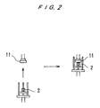
- Fig. 2 is a schematic view illustrating incorporation of a substrate holder with a STM.
- Fig. 3 is a schematic view illustrating a structure for incorporation.
- Fig. 4 is a plane view illustrating positional relationship between a substrate on a substrate holder and projections of a STM.
- Fig. 5 is a STM image of a Ga layer.
-
- As described above, one of the features of preferred embodiments is that a scanning tunneling microscope (STM) is incorporated with a molecular beam epitaxy (MBE) device and observation is performed by the STM in the space where the crystal(s) is in process of MBE growing. In the present invention, the terms of "observation at a state where a crystal(s) is growing" mean STM observation of crystal growth at the atomic level in the same space as one in which MBE crystal growing is proceeding.
- For realizing such observation, in preferred embodiments, a substrate holder placed with a clearance far from a substrate heating system, a heat insulating shield covering a whole of the STM and a STM drive mechanism are provided
- The substrate holder has a wider clearance than a holder generally used has so that vibration transmitted from the MBE can be cut off.
- Since the STM is protected by the heat insulating shield, such influences as from high vapor pressure atmosphere and radiant heat according to substrate heating are suppressed. Especially, a bad effect to a micro-drive mechanism of the STM probe is prevented.
- As illustrated in Fig. 1, in the crystal growth observing apparatus, a substrate holder (11) with a heating system, molecular beam cells (12) and a shroud for liquid nitrogen are provided with a molecular beam epitaxy device: MBE device (1) and are disposed in a vacuum vessel. For moving a scanning runneling microscope: STM (2) upward and downward, a STM drive mechanism (3) is provided.
- As illustrated in Fig. 2, when observation is performed, the STM (2) is moved upward and is incorporated with the substrate holder (11). Crystal growth on the surface of a substrate sample, which is supported by the substrate holder (11) and is in process of MBE crystal growing, is observed by the STM (2).
- As illustrated in Fig. 3, the substrate holder (11), which is one of the parts forming the MBE device (1), holds a substrate (4). A substrate heating system (14) is provided with the substrate holder (11). The substrate holder (11) is supported by the engagement of three pins (15) extending in the horizontal direction from a peripheral surface of a casing of the substrate heating system (14) with notches (16) formed in the casing. The substrate holder (11) is placed apart from the casing of the substrate heating system (14) so as to form a clearance (17) between the substrate holder (11) and side and bottom surfaces of the casing.
- In the STM (2), a STM scanner (24) is covered with a heat insulating shield (21), which protects the STM scanner (24) not only from MBE high vapor pressure atmosphere but also from radiant heat according to substrate heating. Projections (23) are provided at the upper portion of the heat insulating shield (21).
- The STM scanner (24) with micro size can slightly move along the directions of X-Y-Z three axes. A STM probe (22) is secured at the upper portion of the STM scanner (24). When STM observation is performed, the STM probe (22) is projected from the inside of the heat insulating shield (21) and is opposed to the surface of the substrate (4), permitting observation of crystal growth.
- With respect to the projections (23), the shape, number and disposition are not restricted, but a conical or pyramidal shape is preferable. The number is preferably three so as to come into contact with the surface of the substrate holder (11) at three positions. One of three projections (23) can also serve as an electric terminal which permits tunnel current between the substrate holder (11) and the projection. In this case, the projection is insulated from the heat insulating shield (21).
- As illustrated in Fig. 4, three projections (23) are disposed at vertices of a triangle and come into contact with the surface of the substrate holder (11). A projection (23A) among the three serves as an electric terminal.
- The STM drive mechanism (3) causes the STM (2) to move upward in the MBE device (1) preserved at vacuum state and, as illustrated in Fig. 3, causes the projections (23) to come into contact with the surface of the substrate holder (11) opposed thereto at three positions. Subsequently, the STM drive mechanism (3) causes the STM probe (22) to dispose close to the surface of the substrate (4) so as to observe crystal growth on the surface of the substrate (4) based on tunnel current.
- The STM drive mechanism (3) causes the STM (2) to move downward in order to house the STM (2) in the shroud for liquid nitrogen when observation at a state where a crystal(s) is growing is not necessary, for example, during long-time buffer growth.
- A narrow pipe(s) into which wiring of the STM (2) is inserted may be provided in the strut of the STM drive mechanism (3) so that the MBE (1) can be connected to a control device disposed at the outside of the MBE device (1).
- The narrow pipe can also protect the wiring of the STM (2) from electromagnetic noise from the molecular beam cells (12).
- Observation of crystal growth using the above-mentioned apparatus of the present invention will be explained as follows:
- The STM (2) is housed in the lower portion of the MBE device (1) by the STM drive mechanism (3) and a buffer is made to grow with a MBE growing method generally used after cleaning the surface of the substrate (4) supported by the substrate holder (11). The STM (2) is moved upward with the temperature of the sample maintained so as to be incorporated with the substrate holder (11) as illustrated in Fig. 3. The substrate holder (11) is separated from the substrate heating system (14) of the MBE device (1). The substrate holder (11) itself is incorporated with the STM (2) and is placed with the wide clearance (17) formed between the substrate holder (11) and the substrate heating system (14). Subsequendy, the STM probe (22) is come into contact with the substrate holder (4) and a STM observation mode is prepared.
- Raw materials are supplied in the MBE in order to perform STM observation by opening a shutter of the molecular beam cells (12).
- According to the present invention, condition searching for producing a quancum nano structure will be facilitated and a quantum nano structure with the regulated size will be produced.
- Elucidation of the principle of a crystal growing mechanism will be also promoted.
- Improvement of the quality of quantum nano structure, which has been considered to be difficult, will be realized, control of the size will be facilitated, and devices with a quantum nano structure will be developed. In addition, a new nano-drawing such as a temporary patterning together with crystal growth by scanning the probe (22) of the STM (2) will be possible.
- The present invention also includes feasibility to produce quite a new growing mechanism according to the effect of high electric field between the probe and the sample, which is derived from a tunneling phenomenon.
- Ga crystals were made to grow on a GaAs (001) substrate using the crystal growth observing apparatus with the structure mentioned above.
- The STM (2) was housed in the lower portion of the MBE device (1) by the STM drive mechanism (3) and a GaAs buffer was made to grow by the MBE growing method after cleaning the surface of the GaAs substrate.
- The STM was moved upward with the temperature of the substrate (4) preserved and the substrate holder (11) was lifted while catching the substrate holder (11) by the projections (23) at three positions opposed to the substrate holder (11).
- The substrate holder (11) was separated from the substrate heating mechanism (14) and was itself incorporated with the STM (2) through the wide clearance formed between the substrate holder (11) and the substrate heating mechanism (14).
- The STM probe (22) was come into contact with the surface of the substrate (4). A STM observation mode was prepared.
- Subsequently, raw materials with the amount of which an atomic layer was formed were supplied by opening the shutter of Ga molecular beam cells. STM observation was performed.
- A plurality of Ga clusters with the diameter of about 1 nm were observed in the observation area with the size of 50 nm × 50 nm. This exposed an initial process of Ga crystal growing.
- Fig. 5 is a STM image obtained immediately after supplying Ga molecular beam on the GaAs (001) substrate in the process of MBE crystal growing at 200 °C.
- The amount of Ga molecular beam can be freely changed. As molecular beam can be temporarily supplied together with Ga molecular beam. Other raw materials such as In can be also supplied. As far as the substrate is conductive, observation will be possible with other substrate than GaAs.
- It is needless to say that the present invention is not restricted to the example.
Claims (3)
- An apparatus for observing crystal growth, comprising a molecular beam epitaxy device (1) having a vacuum vessel; a scanning tunneling microscope (2) having a probe (22), said scanning tunneling microscope being incorporated with said molecular beam epitaxy device and being protected from vapor pressure atmosphere and radiant heat by a heat insulating shield (21); a substrate holder (11) disposed in said vacuum vessel of the molecular beam epitaxy device, said substrate holder being provided with a substrate heating system (14) and being arranged to be supported only by the scanning tunneling microscope in contact with the substrate holder during observation; and a drive mechanism (3) causing the scanning tunneling microscope to move back and forth while leaving the scanning tunneling microscope opposed to said substrate holder.
- The apparatus as claimed in claim 1, wherein the substrate holder is connected to a casing of said substrate heating system with a clearance (17) and is arranged such that the connection is released during observation so that the substrate holder is supported only by the scanning tunneling microscope.
- The apparatus as claimed in claim 2, wherein pins (15) are provided with said casing of the substrate heating system and the substrate holder is connected to the casing by engagement of said pins with notches (16) formed in the casing.
Priority Applications (1)
| Application Number | Priority Date | Filing Date | Title |
|---|---|---|---|
| DK98310092T DK0936291T3 (en) | 1997-12-10 | 1998-12-09 | Crystal Growth Monitoring Device |
Applications Claiming Priority (2)
| Application Number | Priority Date | Filing Date | Title |
|---|---|---|---|
| JP34041397A JP3188913B2 (en) | 1997-12-10 | 1997-12-10 | Crystal growth observation device |
| JP34041397 | 1997-12-10 |
Publications (2)
| Publication Number | Publication Date |
|---|---|
| EP0936291A1 EP0936291A1 (en) | 1999-08-18 |
| EP0936291B1 true EP0936291B1 (en) | 2005-04-06 |
Family
ID=18336716
Family Applications (1)
| Application Number | Title | Priority Date | Filing Date |
|---|---|---|---|
| EP98310092A Expired - Lifetime EP0936291B1 (en) | 1997-12-10 | 1998-12-09 | Crystal growth observing apparatus |
Country Status (5)
| Country | Link |
|---|---|
| US (1) | US6074485A (en) |
| EP (1) | EP0936291B1 (en) |
| JP (1) | JP3188913B2 (en) |
| DE (1) | DE69829641T2 (en) |
| DK (1) | DK0936291T3 (en) |
Families Citing this family (3)
| Publication number | Priority date | Publication date | Assignee | Title |
|---|---|---|---|---|
| US6994750B2 (en) * | 2001-09-10 | 2006-02-07 | Matsushita Electric Industrial Co., Ltd. | Film evaluating method, temperature measuring method, and semiconductor device manufacturing method |
| CN104749325B (en) * | 2015-04-13 | 2016-09-21 | 清华大学 | Transport property measuring method in situ |
| CN111876729B (en) * | 2020-07-02 | 2021-08-13 | 中国科学技术大学 | A STM-MBE Combined System |
Family Cites Families (7)
| Publication number | Priority date | Publication date | Assignee | Title |
|---|---|---|---|---|
| JPS62174699A (en) * | 1986-01-28 | 1987-07-31 | 富士写真フイルム株式会社 | Film for recording |
| US4732108A (en) * | 1986-08-26 | 1988-03-22 | The Perkin-Elmer Corporation | Apparatus for monitoring epitaxial growth |
| US5323003A (en) * | 1991-09-03 | 1994-06-21 | Canon Kabushiki Kaisha | Scanning probe microscope and method of observing sample by using such a microscope |
| JPH05203406A (en) * | 1992-01-24 | 1993-08-10 | Sony Corp | Stm-fim-mbe composite device |
| US5582646A (en) * | 1994-10-21 | 1996-12-10 | J.A. Woollam Co. Inc. | Ellipsometer/polarimeter based process monitor and control system suitable for simultaneous retrofit on molecular beam epitaxy system RHEED/LEED interface system, and method of use |
| US5455420A (en) * | 1994-07-12 | 1995-10-03 | Topometrix | Scanning probe microscope apparatus for use in a scanning electron |
| JP2912842B2 (en) * | 1995-01-17 | 1999-06-28 | 株式会社エイコー・エンジニアリング | Thin film forming equipment |
-
1997
- 1997-12-10 JP JP34041397A patent/JP3188913B2/en not_active Expired - Lifetime
-
1998
- 1998-12-08 US US09/206,976 patent/US6074485A/en not_active Expired - Fee Related
- 1998-12-09 DK DK98310092T patent/DK0936291T3/en active
- 1998-12-09 DE DE69829641T patent/DE69829641T2/en not_active Expired - Lifetime
- 1998-12-09 EP EP98310092A patent/EP0936291B1/en not_active Expired - Lifetime
Also Published As
| Publication number | Publication date |
|---|---|
| DE69829641D1 (en) | 2005-05-12 |
| DK0936291T3 (en) | 2005-04-25 |
| JP3188913B2 (en) | 2001-07-16 |
| DE69829641T2 (en) | 2005-09-08 |
| US6074485A (en) | 2000-06-13 |
| EP0936291A1 (en) | 1999-08-18 |
| JPH11171692A (en) | 1999-06-29 |
Similar Documents
| Publication | Publication Date | Title |
|---|---|---|
| Chan et al. | ZnSe nanowires epitaxially grown on GaP (111) substrates by molecular-beam epitaxy | |
| EP0430280B1 (en) | Selective and non-selective deposition of Si1-x Gex on a Si substrate that is partially masked with Si O2 | |
| JP3997827B2 (en) | Gallium nitride growth substrate, gallium nitride growth substrate manufacturing method, and gallium nitride substrate manufacturing method | |
| TWI313087B (en) | ||
| TW201603119A (en) | Method for obtaining a planar semi-polar gallium nitride surface | |
| Kubler et al. | Si adatom surface migration biasing by elastic strain gradients during capping of Ge or Si 1− x Ge x hut islands | |
| Honda et al. | Transmission electron microscopy investigation of dislocations in GaN layer grown by facet-controlled epitaxial lateral overgrowth | |
| Derrien et al. | Semiconducting silicide-silicon heterostructures: growth, properties and applications | |
| US6074485A (en) | Crystal growth observing apparatus using a scanning tunneling microscope | |
| Matyi et al. | Microstructural characterization of patterned gallium arsenide grown on< 001> silicon substrates | |
| Williams et al. | Structure of CdTe‐Cd1− x Mn x Te multiple quantum wells grown on (001) InSb substrates by molecular beam epitaxy | |
| Smathers et al. | Enabling in situ atomic-scale characterization of epitaxial surfaces and interfaces | |
| Wang et al. | Molecular-beam epitaxial growth and surface characterization of GaAs (311) B | |
| JP2003300800A (en) | Method for manufacturing nitride semiconductor wafer of element of group iii | |
| JPH021115A (en) | Formation of crystal | |
| Banhart et al. | Dislocation generation in silicon grown laterally over SiO2 by liquid phase epitaxy | |
| Nishida et al. | Step-flow metalorganic vapor phase epitaxy of GaN on SiC substrates | |
| Yanagiya et al. | Self-formed silicon quantum wires on ultrasmooth sapphire substrates | |
| JP2003081696A (en) | Group III nitride crystal with observation function, growth apparatus, method, and device | |
| Nomura et al. | Lateral growth of GaAs on patterned {-1-1-1} B substrates for the fabrication of nano wires using metalorganic molecular beam epitaxy | |
| Heinecke et al. | Evidence for vertical superlattices grown by surface selective growth in MOMBE (CBE) | |
| Latyshev et al. | UHV reflection electron microscopy investigation of the monoatomic steps on the silicon (111) surface at homo-and heteroepitaxial growth | |
| Simão et al. | Scanning tunneling microscopy study of the initial stages of growth of Cu/Si (111): The formation and thermal evolution of the quasi-“5× 5” incommensurate structure | |
| JP3441051B2 (en) | Tip and cantilever used for atomic force microscope, tunnel microscope or spin-polarized tunnel microscope, and method for producing the same | |
| JP2000260711A (en) | Semiconductor substrate manufacturing method |
Legal Events
| Date | Code | Title | Description |
|---|---|---|---|
| PUAI | Public reference made under article 153(3) epc to a published international application that has entered the european phase |
Free format text: ORIGINAL CODE: 0009012 |
|
| AK | Designated contracting states |
Kind code of ref document: A1 Designated state(s): CH DE DK GB IT LI SE |
|
| AX | Request for extension of the european patent |
Free format text: AL;LT;LV;MK;RO;SI |
|
| 17P | Request for examination filed |
Effective date: 19991224 |
|
| AKX | Designation fees paid |
Free format text: CH DE DK GB IT LI SE |
|
| 17Q | First examination report despatched |
Effective date: 20020802 |
|
| GRAP | Despatch of communication of intention to grant a patent |
Free format text: ORIGINAL CODE: EPIDOSNIGR1 |
|
| GRAS | Grant fee paid |
Free format text: ORIGINAL CODE: EPIDOSNIGR3 |
|
| GRAA | (expected) grant |
Free format text: ORIGINAL CODE: 0009210 |
|
| AK | Designated contracting states |
Kind code of ref document: B1 Designated state(s): CH DE DK GB IT LI SE |
|
| REG | Reference to a national code |
Ref country code: GB Ref legal event code: FG4D |
|
| REG | Reference to a national code |
Ref country code: CH Ref legal event code: EP |
|
| REG | Reference to a national code |
Ref country code: DK Ref legal event code: T3 |
|
| REF | Corresponds to: |
Ref document number: 69829641 Country of ref document: DE Date of ref document: 20050512 Kind code of ref document: P |
|
| REG | Reference to a national code |
Ref country code: SE Ref legal event code: TRGR |
|
| REG | Reference to a national code |
Ref country code: CH Ref legal event code: NV Representative=s name: A. BRAUN, BRAUN, HERITIER, ESCHMANN AG PATENTANWAE |
|
| PLBE | No opposition filed within time limit |
Free format text: ORIGINAL CODE: 0009261 |
|
| STAA | Information on the status of an ep patent application or granted ep patent |
Free format text: STATUS: NO OPPOSITION FILED WITHIN TIME LIMIT |
|
| 26N | No opposition filed |
Effective date: 20060110 |
|
| REG | Reference to a national code |
Ref country code: CH Ref legal event code: PFA Owner name: NATIONAL RESEARCH INSTITUTE FOR METALS Free format text: NATIONAL RESEARCH INSTITUTE FOR METALS#1-2-1 SENGEN#TSUKUBA-SHI, IBARAKI (JP) -TRANSFER TO- NATIONAL RESEARCH INSTITUTE FOR METALS#1-2-1 SENGEN#TSUKUBA-SHI, IBARAKI (JP) |
|
| PGFP | Annual fee paid to national office [announced via postgrant information from national office to epo] |
Ref country code: DK Payment date: 20101210 Year of fee payment: 13 |
|
| PGFP | Annual fee paid to national office [announced via postgrant information from national office to epo] |
Ref country code: GB Payment date: 20101221 Year of fee payment: 13 |
|
| PGFP | Annual fee paid to national office [announced via postgrant information from national office to epo] |
Ref country code: SE Payment date: 20111223 Year of fee payment: 14 Ref country code: CH Payment date: 20111227 Year of fee payment: 14 |
|
| PGFP | Annual fee paid to national office [announced via postgrant information from national office to epo] |
Ref country code: DE Payment date: 20111222 Year of fee payment: 14 |
|
| PGFP | Annual fee paid to national office [announced via postgrant information from national office to epo] |
Ref country code: IT Payment date: 20111227 Year of fee payment: 14 |
|
| PG25 | Lapsed in a contracting state [announced via postgrant information from national office to epo] |
Ref country code: SE Free format text: LAPSE BECAUSE OF NON-PAYMENT OF DUE FEES Effective date: 20121210 |
|
| REG | Reference to a national code |
Ref country code: CH Ref legal event code: PL |
|
| REG | Reference to a national code |
Ref country code: DK Ref legal event code: EBP |
|
| GBPC | Gb: european patent ceased through non-payment of renewal fee |
Effective date: 20121209 |
|
| REG | Reference to a national code |
Ref country code: DE Ref legal event code: R119 Ref document number: 69829641 Country of ref document: DE Effective date: 20130702 |
|
| PG25 | Lapsed in a contracting state [announced via postgrant information from national office to epo] |
Ref country code: CH Free format text: LAPSE BECAUSE OF NON-PAYMENT OF DUE FEES Effective date: 20121231 Ref country code: DE Free format text: LAPSE BECAUSE OF NON-PAYMENT OF DUE FEES Effective date: 20130702 Ref country code: LI Free format text: LAPSE BECAUSE OF NON-PAYMENT OF DUE FEES Effective date: 20121231 |
|
| PG25 | Lapsed in a contracting state [announced via postgrant information from national office to epo] |
Ref country code: GB Free format text: LAPSE BECAUSE OF NON-PAYMENT OF DUE FEES Effective date: 20121209 |
|
| PG25 | Lapsed in a contracting state [announced via postgrant information from national office to epo] |
Ref country code: IT Free format text: LAPSE BECAUSE OF NON-PAYMENT OF DUE FEES Effective date: 20121209 |
|
| PG25 | Lapsed in a contracting state [announced via postgrant information from national office to epo] |
Ref country code: DK Free format text: LAPSE BECAUSE OF NON-PAYMENT OF DUE FEES Effective date: 20130102 |