EP0929915B1 - Connectors having improved crosstalk and signal transmission characteristics - Google Patents
Connectors having improved crosstalk and signal transmission characteristics Download PDFInfo
- Publication number
- EP0929915B1 EP0929915B1 EP98937224A EP98937224A EP0929915B1 EP 0929915 B1 EP0929915 B1 EP 0929915B1 EP 98937224 A EP98937224 A EP 98937224A EP 98937224 A EP98937224 A EP 98937224A EP 0929915 B1 EP0929915 B1 EP 0929915B1
- Authority
- EP
- European Patent Office
- Prior art keywords
- connector
- female
- contact
- conductive
- panel
- Prior art date
- Legal status (The legal status is an assumption and is not a legal conclusion. Google has not performed a legal analysis and makes no representation as to the accuracy of the status listed.)
- Expired - Lifetime
Links
Images


Classifications
-
- H—ELECTRICITY
- H01—ELECTRIC ELEMENTS
- H01R—ELECTRICALLY-CONDUCTIVE CONNECTIONS; STRUCTURAL ASSOCIATIONS OF A PLURALITY OF MUTUALLY-INSULATED ELECTRICAL CONNECTING ELEMENTS; COUPLING DEVICES; CURRENT COLLECTORS
- H01R13/00—Details of coupling devices of the kinds covered by groups H01R12/70 or H01R24/00 - H01R33/00
- H01R13/648—Protective earth or shield arrangements on coupling devices, e.g. anti-static shielding
- H01R13/658—High frequency shielding arrangements, e.g. against EMI [Electro-Magnetic Interference] or EMP [Electro-Magnetic Pulse]
- H01R13/6581—Shield structure
- H01R13/6585—Shielding material individually surrounding or interposed between mutually spaced contacts
- H01R13/6589—Shielding material individually surrounding or interposed between mutually spaced contacts with wires separated by conductive housing parts
-
- H—ELECTRICITY
- H01—ELECTRIC ELEMENTS
- H01R—ELECTRICALLY-CONDUCTIVE CONNECTIONS; STRUCTURAL ASSOCIATIONS OF A PLURALITY OF MUTUALLY-INSULATED ELECTRICAL CONNECTING ELEMENTS; COUPLING DEVICES; CURRENT COLLECTORS
- H01R13/00—Details of coupling devices of the kinds covered by groups H01R12/70 or H01R24/00 - H01R33/00
- H01R13/648—Protective earth or shield arrangements on coupling devices, e.g. anti-static shielding
- H01R13/658—High frequency shielding arrangements, e.g. against EMI [Electro-Magnetic Interference] or EMP [Electro-Magnetic Pulse]
- H01R13/6581—Shield structure
- H01R13/6585—Shielding material individually surrounding or interposed between mutually spaced contacts
- H01R13/6588—Shielding material individually surrounding or interposed between mutually spaced contacts with through openings for individual contacts
-
- H—ELECTRICITY
- H01—ELECTRIC ELEMENTS
- H01R—ELECTRICALLY-CONDUCTIVE CONNECTIONS; STRUCTURAL ASSOCIATIONS OF A PLURALITY OF MUTUALLY-INSULATED ELECTRICAL CONNECTING ELEMENTS; COUPLING DEVICES; CURRENT COLLECTORS
- H01R13/00—Details of coupling devices of the kinds covered by groups H01R12/70 or H01R24/00 - H01R33/00
- H01R13/648—Protective earth or shield arrangements on coupling devices, e.g. anti-static shielding
- H01R13/658—High frequency shielding arrangements, e.g. against EMI [Electro-Magnetic Interference] or EMP [Electro-Magnetic Pulse]
- H01R13/6598—Shield material
- H01R13/6599—Dielectric material made conductive, e.g. plastic material coated with metal
-
- H—ELECTRICITY
- H01—ELECTRIC ELEMENTS
- H01R—ELECTRICALLY-CONDUCTIVE CONNECTIONS; STRUCTURAL ASSOCIATIONS OF A PLURALITY OF MUTUALLY-INSULATED ELECTRICAL CONNECTING ELEMENTS; COUPLING DEVICES; CURRENT COLLECTORS
- H01R13/00—Details of coupling devices of the kinds covered by groups H01R12/70 or H01R24/00 - H01R33/00
- H01R13/66—Structural association with built-in electrical component
- H01R13/665—Structural association with built-in electrical component with built-in electronic circuit
- H01R13/6658—Structural association with built-in electrical component with built-in electronic circuit on printed circuit board
Definitions
- Modem backplanes serve as communication media for the exchange of electronic signals between a plurality of daughter cards.
- the daughter cards generate communication signals, for example, data signals, address signals, and control signals which are distributed to daughter card connectors mounted on one or both sides of each daughter card.
- the daughter card connectors register with a corresponding set of backplane connectors on the backplane, which in turn distributes the signals between daughter cards along various communication paths.
- Each connector pair includes an array of conductive interconnects in the form of mating male pins and female contacts which couple by frictional contact.
- the interconnects each provide a separate electrical path for the transmission of signals between, boards typically with some providing the transmission of signals in one direction and the others providing the transmission of signals in the other direction.
- the interconnect paths run substantially parallel.
- This configuration includes a male connector housing 30 having an array of male pins 36 mounted to a backplane 32 and a corresponding female connector housing 34 having a corresponding array of female contacts 38 bonded to a printed circuit board daughter card 42.
- the female contacts 38 connect to the printed circuit board 42 by metal rods 40 which are bent approximately at right angles 44 contacting the printed wiring through plated through-holes 46 or surface mount pads.
- FIG. 1B illustrates the path of a signal, represented by arrow 48, propagating between a backplane 32 and a daughter card 42 through a prior art connector assembly 30, 34. It is apparent that the path length of the conductive medium between boards, including male pin 36A, female contact 38A and metal rod 40A, is extended and linear. It is also apparent that this path is parallel to adjacent paths defined by male pin 46B, female contact 38B and metal rod 40B over its entire length. The behavior of the signal current 48 and its responsibility in inducing crosstalk are illustrated in Prior Art FIG. 2 and FIG. 3.
- Prior Art FIG. 2 illustrates signal current 48 propagating through a male pin 36, entering a female contact 38 at contact point 52 and passing to conducting rod 40. As the signal propagates, it generates an H field 53 represented in the drawing in exemplary fashion as entering the plane of the page at points 49 and exiting the plane of the page at points 51.
- the H field 53 is illustrated in the perspective view of Prior Art FIG. 3. E fields are not shown, but they are also generated by the voltages on the conductors.
- H fields 53A, 53B, 53C respectively generated by signal currents 48A, 48B, 48C emanate in a generally cylindrical orientation about the signal path, with the circles representing each field at a particular axial location along the conductive paths as shown.
- the resultant H field 53A generated by one signal 48A may extend spatially far enough to influence a signal 40B of an adjacent path and a signal 40C of a non-adjacent path.
- This form of coupling is referred to in the art as inductive coupling.
- the electric field created by the first signal 48A may couple to nearby signal paths 48B, 48C. This is known in the art as capacitive coupling. In this manner each of signals 48A, 48B, 48C may influence adjacent or non-adjacent signals.
- a conductive medium has an inherent inductance caused by an H field generated about the medium by the current flowing through it. The closer a first medium is placed in proximity to a second medium, the more likely their respective H fields will influence each other. This, in turn, leads to an increased likelihood of crosstalk between media.
- the controlled-impedance lines of predominantly inductive prior art connectors are generally not matched between the backplane and daughter card, causing reflections when signal rise times approach the propagation delay of the connector paths. This causes signal distortion and attenuation and increases crosstalk due to multiple reflections, limiting high-frequency throughput.
- Shielded connectors are available to enhance throughput, but generally are expensive to produce and have relatively poor contact density per unit area.
- a shield is typically placed between each row of contacts on each side (male and female) of the connector, a very complicated and expensive configuration. In this configuration, H field attenuation is provided by providing ground return paths adjacent each forward signal path. E field attenuation is not fully effective because the resultant shield geometry is suboptimal. This phenomenon is detailed in Hybricon's Technology Focus publication H89107, incorporated herein by reference, which explains crosstalk for two parallel conductive paths.
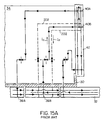
- FIG. 15A is a side view of a conventional shielded connector, illustrating current flow in adjacent signal paths.
- a backplane 32 includes a male connector 30 and a daughter card includes a corresponding female connector 34.
- Planar shields 202 are inserted between rows or columns (for example along the vertical cross section of FIG. 1B) of mated contacts 36A, 40A, and 36B, 40B, in such a manner that return currents I R between mating boards will pass through the shields, and thereby cancel or attenuate the H fields generated by the forward currents IF through the signal contacts.
- E fields generated by the voltage on the contacts are likewise terminated by the shields 202. This is analogous to the manner by which the E fields and H fields are contained by stripline traces on a printed circuit board.
- signals are configured in the connector such that the nearest paths to a given forward signal path are return paths.
- This causes the H fields of nearest paths to be in opposite orientations, thereby tending to reduce the overall H fields which couple to other paths.
- the opposite potential also tends to reduce the respective E fields.
- This technique is somewhat effective but results in the wasteful use of pins as the return paths that are generally connected to the ground plane.
- the present invention is directed to a connector assembly and method for forming such an assembly which effectively mitigates the hazards of crosstalk between adjacent signal paths in an economic manner. Furthermore, transmission path characteristics are improved to achieve overall improvement of signal transmission at higher speeds.
- Crosstalk and propagation delay are reduced in the present invention by configuring the connector to provide for cancellation or reduction of electromagnetic fields (H or B fields), in part by self cancellation, and independently of the electric fields (E fields).
- H or B fields electromagnetic fields
- E fields electric fields
- the present invention includes a female contact, or pin, having a proximal end and a distal end.
- the distal end is adapted to conductively engage a mating male pin inserted at and electrically insulated from the proximal end.
- a region of the female pin and the male pin are electromagnetically coupled.
- a signal propagating through the connector generates a first H field of a first orientation about the male pin. At the contact point, this signal reverses direction and generates a second H field of a second orientation about the female pin.
- the first and second orientations of the H fields are substantially opposite which, in turn, causes the first and second H fields to substantially cancel in the region of electromagnetic interaction.
- a conductor is coupled to the proximal end of the female pin.
- the conductor is substantially removed from the region of electromagnetic interaction and is shielded by ground planes such that the third magnetic field generated by the signal propagating through the conductor avoids interference with the cancellation of the first and second magnetic fields in the region.
- the conductor is preferably formed in a flexible circuit panel.
- the panel is preferably mounted to an "L" or "U”-shaped substrate such that the circuit panel and the conductors fold from a front face of the connector at the proximal end of the female pin to a side face of a connector.
- a preferred connector embodiment includes a plurality of female pins supported by a female connector housing and adapted to mate with a like plurality of male pins mounted on a corresponding male connector housing.
- Each mated male pin and female contact are contained in cavities of plastic plated with a conductive metal which effectively shields the E fields of each mated pin/contact from the adjacent contacts.
- the present invention cancels out the H field of the signal, allowing the E fields to be confined with a simple electrostatic shield in the form of the plastic walls of the cavity and/or conductive plating mounted therein.
- the flexible circuit panel includes a plurality of conductors for conducting signals from the proximal end of the female contacts to an array of plated through-holes at a side face of the connector.
- the conductors and ground planes form controlled impedance stripline transmission lines.
- a ground reference is provided in close proximity to either side of the conductors.
- the contact pins are employed as terminals at the side face.
- the contact pins preferably comprise split roll pins in the form of a tubular malleable conductor having a longitudinal slot and a lateral slot.
- the longitudinal slot allows for compression and expansion of the roll pin in a mounting hole, for example a plated through-hole.
- the lateral slot allows for the roll pin to be mounted between first and second plated through-holes of different diameters.
- FIGs. 1A and 1B are perspective and side views respectively of a prior art connector configuration.
- FIG. 2 is a close-up cutaway side view of the interface between the male pin and female contact of the prior art connector of FIG. 1A illustrating signal current flow and the resulting magnetic field in the region of the connector.
- FIG. 3 is a perspective view of the interface of FIG. 2 illustrating crosstalk arising from electromagnetic interaction of adjacent signal paths.
- FIG. 4 is an exploded perspective view of a connector assembly in accordance with a preferred embodiment of the present invention.
- FIG. 5 is a close-up cutaway side view of the interface between the male pin and female pin of a preferred connector embodiment illustrating signal flow through the interface and the resulting offsetting magnetic fields in accordance with the present invention.
- FIG. 6 is a perspective view of the interface of FIG. 5 illustrating cancellation of the magnetic fields in the region of the magnetic interaction in accordance with the present invention.
- FIG. 7 is a perspective view of a preferred embodiment of a flexible circuit panel mounted to a contact and roll pin alignment substrate in accordance with the present invention.
- FIGs. 8A and 8B are perspective views of preferred embodiments of female contacts in accordance with the present invention.
- FIG. 9 is a cutaway side view of second preferred embodiment of a female contact interfacing with a male pin.
- FIG. 10 is a perspective view of a roll-pin in accordance with the present invention.
- FIG. 11 is a perspective view of a plated through-hole in accordance with the present invention.
- FIG. 12 is a perspective view of a roll-pin used for interconnecting two boards in accordance with the present invention.
- FIG. 13 is a perspective view of an alternative embodiment of a male pin connector housing in accordance with the present invention.
- FIGs. 14A and 14B are side views of alternative female connector configurations in accordance with the present invention.
- FIG. 15A is a schematic side view of a conventional shielded connector, illustrating the directions of forward and reverse current flow.
- FIG. 15B is a schematic side view of a connector in accordance with the present invention, illustrating self-cancellation of H fields, allowing for simple shielding of E fields.
- FIG. 16 is a side view of an alternative shielding configuration, in accordance with the present invention.
- the present invention mitigates the effect of crosstalk in a connector by reducing the extent of electromagnetic field coupling between signal paths.
- a signal traversing through a connector of the present invention generates a first magnetic field of a first orientation as it propagates along a male pin to a point of contact at a distal end of a female connector, and likewise generates a second magnetic field of a second orientation substantially opposite the first orientation as the signal propagates along the body of the female connector to a termination point at a proximal end of the female connector.
- a folded signal path is provided, causing the first and second opposed magnetic fields of the signal to essentially cancel. This in turn reduces or eliminates the likelihood that the signal propagating through the connector region will influence the propagation of nearby signals. This also reduces the self-inductance of the path, thereby reducing frequency-dependent attenuation of the path.
- the present invention further provides isolation between electric fields of each contact in the form of electrostatic shielding, comprising conductive plating in the plastic cavities housing the female contacts. Because the signals traversing the male pin and female pin, or contact, enter and exit the cavity at the open end, construction of the shielded cavities is relatively straightforward and inexpensive, thereby extending the useful frequency range of the connector in an economical manner.
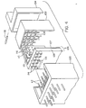
- FIG. 4 is a perspective illustration of a first preferred connector embodiment in accordance with the present invention.
- the embodiment includes a male connector housing 100 having an array of male pins 112.
- a female connector housing 102 includes a corresponding array of female contacts 110 mounted in corresponding cavities 108.
- the array of female pins, or contacts 110 registers with the array of male pins 112.
- the housings 100, 102 include guides (not shown) or other features which assure alignment of their respective pins 112 and contacts 110.
- the male pins 112 pass through holes 114 in a flexible circuit panel and substrate assembly 106.
- the holes 114 are aligned with the proximal ends of the female contacts 110.
- the proximal ends are electrically coupled to corresponding conductive paths 115 formed on the flexible circuit panel and substrate assembly 106 as illustrated and described in further detail below in conjunction with FIGs. 5-7.
- the assembly 106 comprises a dielectric substrate 109 supporting a circuit panel 107 having multiple conductive paths 115 formed in layers.
- the circuit panel 107 may be provided on the inside face of the substrate as shown in FIG. 4, or preferably, on the outside face as shown in FIGs. 5 and 6, described below. The outside face is preferred to further lengthen the region of magnetic field cancellation, as will be described below.
- Each conductive path 115 in the flexible circuit panel 107 serves as a communication medium between a female contact 110 and a corresponding terminal pin 118 mounted on the connector at right angles to each other, allowing signals to pass from an edge of the daughter card to its surface, as in the prior art.
- the present invention accomplishes this in a controlled impedance environment with minimal crosstalk, because ground plane layers on either side of the conductive path layers provide a controlled-impedance stripline environment on the panel 107.
- assembly 106 is "U" shaped to add rigidity to the connector structure.
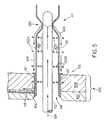
- FIG. 5 is a close-up cutaway side view of the interface between the male pin 112 and the female contact 110 illustrating a preferred connector configuration of the present invention.
- a signal 124 propagates through the male pin 112 to a contact area 120 at a distal end 111 of the female contact 110.
- the signal 124 branches out and reverses direction along the walls of the female contact 110. From there, the signal 124 propagates along the conductive material of the plated through-hole 121, and further along stripline conductor 115 of the flexible circuit panel 107.
- the signal 124 As the signal 124 propagates in the first direction along male pin 112, it generates a magnetic field 150 oriented in a first direction about the surface of the pin 112 as shown. Likewise, as the signal 124 propagates in the second direction along the body of the female contact 110, it generates a second magnetic field 152A, 152B, oriented in a second direction as shown.
- the first magnetic field 150 and second magnetic field 152 are oriented in substantially opposite directions such that they tend to substantially cancel each other. This reduces the extent of the net magnetic field outside of the region of contact such that the net field is insufficient for inducing crosstalk with signals of nearby interconnect paths, thereby mitigating the likelihood of crosstalk.
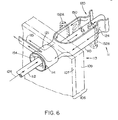
- the orientation of the respective magnetic fields 150, 152 is more clearly illustrated in the perspective view of FIG. 6 where it is shown that signal 124 propagating along male pin 112 generates a magnetic field oriented in a clockwise direction, a portion of which is illustrated at 150.
- the signal reverses direction and propagates along the body of the female contact 110, generating a magnetic field 152 oriented in a counterclockwise direction as shown.
- the body of the female connector divided into two segments, forming two conductive paths, resulting in first and second counterclockwise magnetic fields, portions of which are shown at 152A, 152B respectively.
- the segmented signal recombines and propagates through plated material of through-hole 116 and conductor 115 to another portion of the flexible circuit panel 107.
- Sloped guides 154 may be formed on the face of the substrate 109 to further pin/contact alignment.
- FIG. 15B is a schematic side view of a connector, illustrating self-cancellation of H fields, and allowing for simple shielding of E fields, in accordance with the present invention.
- a female connector housing 102 and flexible circuit panel are mounted to an edge of a daughter card 42, and a male connector 160 is mounted to a backplane 32.
- this illustration is for purposes of example, and a number of configurations are possible.
- the female connector may be mounted to the backplane and the male connector mounted to the daughter card, or the connectors may be mounted to mating PC boards, etc.
- the male pins and female contacts mate (illustrated schematically by contact point 206) to provide a signal path as shown by arrows 204.
- the signal 204 propagates along backplane 32, through male pin 112, to contact point 206.
- the signal 204 reverses direction and propagates along female contact 110, through flexible circuit panel 107, to press fit contact 116, and into the daughter card 42.
- the signal 204 is preferably shielded by conventional stripline shielding 208 in the backplane 32, flexible circuit panel 107 and daughter card 42.
- signal propagation through the contact chamber region 108 is adapted to cancel the H fields, by virtue of the folded path geometry.
- Cancellation of H fields of the signal 204 in the contact chamber 108 is provided along the interface of the male pin 112 and female contact 110 to the point 210 where the female contact 110 makes contact with the conductor on the flexible circuit panel 107.
- the reverse current 204B on the female contact deviates from the forward current 204A on the male pin 112, and cancellation of the H field ceases. It is therefore preferable to position the portion of the flexible panel 107 running parallel to the backplane 32, as close to the backplane as possible.
- E field shielding is accomplished via a conductive shield 167 preferably formed by a plating or coating on the surfaces of the chambers 108 which encompass the contact area, and is in low resistance contact with a ground plane return path 214. This is described below in detail with reference to FIG. 9.
- the shield 167 is effectively at the circuit ground potential and effectively contains the E field of the signal.
- the conductive honeycomb 102 can be implemented in many ways. In the preferred embodiment, the honeycomb is molded in plastic, upon which copper is deposited, along with additional copper plating over the copper deposition. Solder or other metal is plated over the copper for solderability. Other formation techniques are equally applicable.
- the metallic plating forming the shield 167 provides a double wall of conductive material between each signal contact, for example between the contacts of chamber 108 and adjacent chamber 108A, in adjacent rows and columns. As seen in FIG. 9, the female contact thus is substantially enclosed by a conductive material, with each wall providing an independent path for capacitive currents.
- Capacitors 216 (see FIG. 9) schematically represent the continuous stray capacitance between the female contact 110 and the surface of the conductive metal plating 167 of the shield. There are currents flowing through these stray capacitances which are functions of the amount of capacitance and the rate of change of the differences in voltage at each location of the contact 110, and corresponding locations on the shield 167.
- the shield adjacent each contact eliminates, or substantially reduces, the E fields produced by these voltages so that cross coupling between neighboring contacts is essentially eliminated.
- the currents produce electromagnetic fields which are substantially eliminated by eddy currents induced in the adjacent shields surrounding neighboring pins.
- the E field shield carry return currents, as is the case in the prior art shielded connector configuration shown in FIG. 15A, in which the shields are fabricated in two parts with integral mating contacts to provide return paths for both E and H fields simultaneously.
- This important difference, and the folded shape of the contact path, allows the E shield of the present invention to be molded or otherwise fabricated as a single part, reducing manufacturing costs of the shield considerably as compared to conventional configurations.
- the opening of the female contact at its "proximal end" avoids contact with the male pin. If contact is made, accidentally or otherwise, at the opening, then the interface would effectively operate as a short pin. This would not prevent the connector from functioning; but if accidental, any contact may generate noise in the signal.
- proximal end and distal end are used above to describe portions of a preferred embodiment of the female contact, such terms are interchangeable with “first end” and “second end” in alternative embodiments and do not necessarily describe their relative spatial positions.
- the male pin may make contact with the female contact near its opening, and the female contact may be shaped to fold back on itself, thereby providing the "folded path" geometry of the present invention.
- FIG. 7 is a perspective view of a circuit panel and substrate assembly 106 in accordance with the present invention.
- the circuit panel and substrate assembly 106 includes an "L"-shaped dielectric substrate 109 which supports a flexible circuit panel 107.
- the circuit panel 107 comprises a plurality of conductive paths 115 which conduct signals from the female contacts on a face 190 of the panel, past corner 156 to terminal holes 116 on a side leg 192 of the assembly.
- the conductive paths 115 are spaced apart such that signals propagating thereon do not interfere with each other.
- the flexible circuit panel 107 is preferably formed in a stripline or microstrip circuit configuration to suppress interference. Ground planes on the panel are generally continuous, except in the region of the contact clearance holes 114 to avoid contact with the signals.
- the circuit panel 107 may be mounted to the inside face of the substrate 109 as shown in FIG. 7, or to the outside face as shown in FIG. 5.
- the invention may also be implemented using standard single or multiple layered rigid printed circuit techniques where the rigid circuit board is shaped as necessary, referred to herein as a "bent-rigid" PC board.
- the rigid circuit board may be provided with or without the rigid substrate 109.
- the circuit panel 107 may be provided using "rigid-flex" technology, where the panel is rigid in the regions of the flat surfaces 190, 192, and flexible at the corner 156.
- the plated contact and terminal holes on the panel 107 may be further plated together with plated through-holes 116 as shown in FIG. 11.
- the though-holes 116 provide a reliable contact between the assembly 106 and the female contacts 110 and roll-pin terminals 118.
- the substrate further provides structure for supporting the female contacts and for holding the contacts in alignment with the shielding chambers.
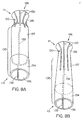
- FIG. 8A is a perspective illustration of a preferred embodiment of the female contact 126 in accordance with the present invention.
- This embodiment includes a continuous cylindrical body 135 having a widened portion 134 at a proximal end near the opening or orifice 136, a tapered body portion 137, and a flared contact location 120 at a distal end.
- the body of the contact is continuous except for a longitudinal slot 132 which permits the contact 126 to adapt to deviations in the mounting surface, assuring a snug fit between the outer surface of non-tapered portion 134 and the inner surface of plated hole 114 (see FIG. 7).
- Slots 130 extend from the tapered body portion 137 to the distal end 111 to form tapered contact leaves 128 which are flared outward beyond contact area 120 as shown.
- the smallest internal diameter between the contact leaves 128 is slightly smaller than the external diameter of the male pin such that the material surfaces of the contact leaves are biased to conductively engage the surface of an inserted male pin.
- the orifice 136 at the proximal end 113 is wider than the remainder of the body to avoid contact with an inserted male pin. Contact at the proximal end could cause intermittent noise and increase insertion force.
- This embodiment is especially well adapted to be press fit in a plated through hole 114 formed on the flexible circuit panel and substrate assembly 106.
- the female contact should be of sufficient length so as to minimize insertion force and to reduce the radii of the contact leaves 128.
- FIG. 8B illustrates an alternative configuration where the body portion 137 is tapered between the opening 136 and contact region 126.
- slots 130 are preferably longer to achieve lower insertion force.
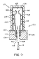
- FIG. 9 is a cutaway side view of a female contact 120 mounted to a flexible circuit panel and substrate assembly 106 and inserted into a connector chamber 108 on the female connector housing 102.
- the contact 110 is mounted to substrate 109 of the flexible circuit and substrate assembly 106 such that a cylindrical portion 160 of dielectric material serves as an insulator between an inserted male pin and the proximal end 113 of the female contact 110.
- the cylindrical portion 160 further serves as a guide during insertion of the male pin. This assures that contact is made in the preferred contact region 120 at the distal end to give the full effect of cancellation of the magnetic fields.
- the wider section of hole 114 can be plated with overlapping conductive material to assure satisfactory contact between the panel 107 and contact 110.
- the chamber 108 walls of the cover 102 are formed of standard connector material 168, for example plastic.
- the inner wall of the chamber is lined with conductive plating 166 which is preferably coupled to ground to serve as a shield for the electric field of the signal propagating along the pin 112 and contact 110 as described above.
- An insulating coating 167 can be applied to the conductive plating 166 to prevent accidental grounding of the female contact 110.
- each chamber 108 is separated by region 260.
- the conductive shield 166 may be applied to the outer surface 262 of the chambers 108 to provide an electric field shielding function.
- the conductive shield may comprise a wire mesh, preferably an insulated wire mesh, in which case, the chamber 108 walls need not be continuous.
- the term "enclosed”, or “substantially enclosed”, as used herein, when referring to the geometry of the chamber, may include a chamber with a solid, continuous wall or alternatively, a wire mesh wall with apertures, in which case, the apertures should be small enough to provide sufficient electrostatic shielding.
- the present invention effectively cancels E-field crosstalk in a simple configuration. This simplicity is especially apparent in the electrostatic shielding 168 of the individual chambers.
- Each cavity 108 is closed at a distal end 171 and open at a proximal end 173.
- a signal enters and exits the chamber at the open proximal end 173 via the inserted male pin 112 and the trace 107 at the face of the female connector 110.
- the distal end 171 and the side walls of the chamber are continuous and closed such that the electrostatic shield 166 can be deposited in the chamber as a continuous layer. This is unlike the conventional configurations where the signal enters at the proximal end 173 and exits at the distal end 171, making electrostatic shielding of conventional connectors complex and expensive.
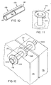
- FIG. 10 is a close-up perspective view of a preferred implementation of terminal 118 shown in FIG. 4 in the form of a roll pin in accordance with the present invention.
- the roll pin 118 of FIG. 10 is generally cylindrical in shape and hollow in cross section and is adapted for coupling the plated through-holes 116 of the flexible circuit board shown in FIG. 4 to a similar hole on a daughter card.
- the body of the roll pin 118 includes a longitudinal slot 140 and a lateral slot 138.
- the longitudinal slot 140 preferably runs the length of the pin 118, whereas the lateral slot 138 cuts across a portion of the circumference of the pin at or near the center of the length of the pin, depending on the application.
- the longitudinal slot 140 allows for the pin body to be circumferentially expanded or compressed in a plated through-hole 116.
- all plated through-holes 116 are of uniform diameter, but in practice, they can vary to a significant degree.
- the lateral slot 138 permits the degree of compression, and thus the outer diameter of the roll pin 118 to be different in each plated through-hole. If one of the holes is axially deeper than the other, the lateral slot can be cut asymmetrically at a position other than the center of the pin, to assure proper contact in each hole.
- FIG. 12 is a perspective illustration of the roll pin 118 of FIG. 10 electrically coupling plated through-holes 116 of first and second circuit boards 174, 176, respectively.
- a first portion 170 of the roll pin 118 is press fit in the through-hole 116A of the first circuit board 174, and a second portion 172 is press fit in a plated through-hole 116D of a second board 176.
- the longitudinal slot 140A of the first portion 170 is wider circumferentially than the longitudinal slot 140B of the second portion 172. This difference in slot width arises because the respective width of the plated through-holes 116A and 116B are different.
- the lateral slot 138 shown in FIG. 9 allows for this difference in longitudinal slot widths as described above.
- crosstalk can arise due to magnetic field coupling (inductive) or electric field coupling (capacitive).
- the magnetic field coupling in the contact region is essentially annulled by the folded geometry illustrated above. Note that the preferred geometry is coaxial using a cylindrical female contact, but all geometries which achieve cancellation are applicable to the present invention.
- any remaining electric field coupling is effectively eliminated by conductive plating 116 in the chamber walls, as shown in FIG. 9.
- a significant advantage of this invention is that the conductive shielding around the region of contact can be provided by a thin conductive plated coating which is inexpensive to deposit. This is because the shield is not required to carry heavier currents associated with reduction of H fields.
- the plating following application, is next insulated, for example conformal coated, to prevent accidental grounding of the signal within the confines of the connector housing. This shielding is deposited on inner and outer surfaces of the housing with an exposed outer plating to provide a ground connection where the two connector housings make contact.
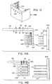
- FIG. 13 is a perspective view of a preferred male connector housing 182 for accomplishing this.
- the housing 182 includes holes 124 for mounting the male pins and rows of spring contacts 122 flanking the two outside pin rows to provide a ground return path.
- the ground springs 122 contact the ground plane of the stripline printed circuit board when the male and female connector assemblies are mated. Each high and low point of the spring contact is dimpled to assure contact at every location.
- Additional holes 183 are conductively plated to contain pins which press fit with the backplane to complete the ground path.
- FIGs 14A and 14B are cutaway side views of alternative embodiments of the present invention.
- the female connector housing 102 is mounted to the substrate assembly 106 such that the side wall of the connector housing 102 and the leg 192 of the assembly 106 are spaced apart as shown.
- input/output transceivers 197 may be mounted to the substrate 106 for energizing signal exchange between boards, thereby reducing signal delay.
- the transceivers 197 may be mounted to the side leg of the substrate assembly 192.
- the male connector housing 100 is adapted to mate with the alternative female connector profiles.
- FIG. 14B illustrates a male connector embodiment having male pins 112 mounted directly to motherboard 100. This configuration is preferred for increasing the magnetic interaction between the signal traversing the male pin 112 and female contact 110. By eliminating the plastic connector material, the region of no interaction (for example, over distance d of FIG. 14A) is reduced or eliminated, enhancing connector performance. Shorter connection paths between the female contacts 110 and conductors on the daughter card 42 are realized in the embodiment of FIG. 14B by mounting roll-pin contacts 118 closer to the face of the female connector 102, for example at the side of the connector housing, as shown.
- the present invention further offers the advantage of a low connector insertion force. This arises because thin materials can be used for the female contact, for example a material of 0.003 inches as compared to prior art female contacts of 0.01 inches. Thin materials are sufficient because in the present invention the contact area is protected on all sides by the chamber walls, including the rear wall of the chamber, unlike conventional configurations.
Landscapes
- Details Of Connecting Devices For Male And Female Coupling (AREA)
- Stereophonic System (AREA)
- Reduction Or Emphasis Of Bandwidth Of Signals (AREA)
Abstract
Description
- Modem backplanes, also referred to as motherboards, serve as communication media for the exchange of electronic signals between a plurality of daughter cards. The daughter cards generate communication signals, for example, data signals, address signals, and control signals which are distributed to daughter card connectors mounted on one or both sides of each daughter card. The daughter card connectors register with a corresponding set of backplane connectors on the backplane, which in turn distributes the signals between daughter cards along various communication paths.
- Each connector pair includes an array of conductive interconnects in the form of mating male pins and female contacts which couple by frictional contact. The interconnects each provide a separate electrical path for the transmission of signals between, boards typically with some providing the transmission of signals in one direction and the others providing the transmission of signals in the other direction. Within a connector, the interconnect paths run substantially parallel.
- As communication technology improves, there is increasing demand on connectors to channel more data through a given area. An obvious solution is to reduce the distance between signal paths, allowing for more data channels. This, however, increases the likelihood of electromagnetic coupling between signals. Such coupling generally takes on two forms, namely electric field E (capacitive) coupling and magnetic field H (inductive) coupling. The influence of either form of coupling between signals is generally referred to in the art as crosstalk. Crosstalk corrupts the waveform of an affected signal, which, in turn, can cause data errors, timing errors or other anomalies which interfere with proper data communication.
- The danger of crosstalk is most significant where signals converge in a densely-populated region as in a connector. This passage of signals through connector pins in close proximity to each other makes crosstalk inevitable in prior art connector configurations, for example the configuration shown in the perspective view of Prior Art FIG. 1A and the side view of Prior Art FIG. 1B. This configuration includes a
male connector housing 30 having an array ofmale pins 36 mounted to abackplane 32 and a correspondingfemale connector housing 34 having a corresponding array offemale contacts 38 bonded to a printed circuitboard daughter card 42. Thefemale contacts 38 connect to the printedcircuit board 42 bymetal rods 40 which are bent approximately atright angles 44 contacting the printed wiring through plated through-holes 46 or surface mount pads. - Such an arrangement is sufficient for transporting signals of moderate speeds. However, in modem systems having faster signal clocks and increased data throughput, crosstalk interferes with system performance. In particular, the length of the paths between the
backplane 32 and thedaughter card 42 and the coupling between them introduces delays, distortions and unwanted couplings which seriously degrade the information transmitted. - Prior Art FIG. 1B illustrates the path of a signal, represented by
arrow 48, propagating between abackplane 32 and adaughter card 42 through a priorart connector assembly male pin 36A,female contact 38A andmetal rod 40A, is extended and linear. It is also apparent that this path is parallel to adjacent paths defined by male pin 46B,female contact 38B andmetal rod 40B over its entire length. The behavior of the signal current 48 and its responsibility in inducing crosstalk are illustrated in Prior Art FIG. 2 and FIG. 3. - Prior Art FIG. 2 illustrates signal current 48 propagating through a
male pin 36, entering afemale contact 38 atcontact point 52 and passing to conductingrod 40. As the signal propagates, it generates anH field 53 represented in the drawing in exemplary fashion as entering the plane of the page atpoints 49 and exiting the plane of the page atpoints 51. TheH field 53 is illustrated in the perspective view of Prior Art FIG. 3. E fields are not shown, but they are also generated by the voltages on the conductors. - In Prior Art FIG. 3,
H fields signal currents resultant H field 53A generated by onesignal 48A may extend spatially far enough to influence asignal 40B of an adjacent path and asignal 40C of a non-adjacent path. This form of coupling is referred to in the art as inductive coupling. Furthermore, the electric field created by thefirst signal 48A, for example, may couple tonearby signal paths signals - It is well known in the art that a conductive medium has an inherent inductance caused by an H field generated about the medium by the current flowing through it. The closer a first medium is placed in proximity to a second medium, the more likely their respective H fields will influence each other. This, in turn, leads to an increased likelihood of crosstalk between media.
- The theory of crosstalk in transmission lines is somewhat involved, but for printed circuit board connectors, the transmission line paths between a backplane and daughter card through male pins and female contacts are sufficiently short such that the signal propagation time is currently generally less than one-half of the rise time of the digital signals transmitted thereon. For this condition, the crosstalk amplitude increases as the signal rise time or frequency component increases. For the same reason, crosstalk increases with connector path length. Furthermore, the male pin/contact paths are characteristically inductive, causing increased signal attenuation as frequency increases. To accommodate high frequencies, or fast rise times, it is common to insert coaxial contact pairs in backplane to daughter card connectors. However, because coaxial pairs are expensive and bulky, they are used only in extraordinary circumstances.
- The controlled-impedance lines of predominantly inductive prior art connectors are generally not matched between the backplane and daughter card, causing reflections when signal rise times approach the propagation delay of the connector paths. This causes signal distortion and attenuation and increases crosstalk due to multiple reflections, limiting high-frequency throughput. Shielded connectors are available to enhance throughput, but generally are expensive to produce and have relatively poor contact density per unit area. To achieve reduction of H and E fields at high frequencies, a shield is typically placed between each row of contacts on each side (male and female) of the connector, a very complicated and expensive configuration. In this configuration, H field attenuation is provided by providing ground return paths adjacent each forward signal path. E field attenuation is not fully effective because the resultant shield geometry is suboptimal. This phenomenon is detailed in Hybricon's Technology Focus publication H89107, incorporated herein by reference, which explains crosstalk for two parallel conductive paths.
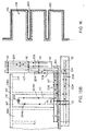
- Prior Art FIG. 15A is a side view of a conventional shielded connector, illustrating current flow in adjacent signal paths. For purposes of example, a
backplane 32 includes amale connector 30 and a daughter card includes a correspondingfemale connector 34.Planar shields 202 are inserted between rows or columns (for example along the vertical cross section of FIG. 1B) ofmated contacts shields 202. This is analogous to the manner by which the E fields and H fields are contained by stripline traces on a printed circuit board. - In another technique for enhancing H field attenuation, signals are configured in the connector such that the nearest paths to a given forward signal path are return paths. This causes the H fields of nearest paths to be in opposite orientations, thereby tending to reduce the overall H fields which couple to other paths. The opposite potential also tends to reduce the respective E fields. This technique is somewhat effective but results in the wasteful use of pins as the return paths that are generally connected to the ground plane.
- These techniques are somewhat effective due to the partial cancellation of the H and E fields between the forward and return paths of each of the signals. However, both approaches reduce signal contact density, which reduces the usefulness of the connector, and raises the cost per signal line through the connector. Other connectors from Vendors such as AMP, Augat, and Teradyne employ complicated stripline contacts to improve performance. However, such connectors are relatively expensive to produce.
- US-A-5, 469, 335, US-A-4, 806, 107 and US-A-2,977,562 are prior art to this application. The present invention is as claimed in the claims.
- The present invention is directed to a connector assembly and method for forming such an assembly which effectively mitigates the hazards of crosstalk between adjacent signal paths in an economic manner. Furthermore, transmission path characteristics are improved to achieve overall improvement of signal transmission at higher speeds.
- Crosstalk and propagation delay are reduced in the present invention by configuring the connector to provide for cancellation or reduction of electromagnetic fields (H or B fields), in part by self cancellation, and independently of the electric fields (E fields). This configuration confers many significant advantages over conventional connectors, including performance, cost, and manufacturability.
- In a first embodiment, the present invention includes a female contact, or pin, having a proximal end and a distal end. The distal end is adapted to conductively engage a mating male pin inserted at and electrically insulated from the proximal end. A region of the female pin and the male pin are electromagnetically coupled. A signal propagating through the connector generates a first H field of a first orientation about the male pin. At the contact point, this signal reverses direction and generates a second H field of a second orientation about the female pin. The first and second orientations of the H fields are substantially opposite which, in turn, causes the first and second H fields to substantially cancel in the region of electromagnetic interaction.
- In a preferred embodiment, a conductor is coupled to the proximal end of the female pin. The conductor is substantially removed from the region of electromagnetic interaction and is shielded by ground planes such that the third magnetic field generated by the signal propagating through the conductor avoids interference with the cancellation of the first and second magnetic fields in the region.
- The conductor is preferably formed in a flexible circuit panel. The panel is preferably mounted to an "L" or "U"-shaped substrate such that the circuit panel and the conductors fold from a front face of the connector at the proximal end of the female pin to a side face of a connector.
- A preferred connector embodiment includes a plurality of female pins supported by a female connector housing and adapted to mate with a like plurality of male pins mounted on a corresponding male connector housing. Each mated male pin and female contact are contained in cavities of plastic plated with a conductive metal which effectively shields the E fields of each mated pin/contact from the adjacent contacts. The present invention cancels out the H field of the signal, allowing the E fields to be confined with a simple electrostatic shield in the form of the plastic walls of the cavity and/or conductive plating mounted therein. The flexible circuit panel includes a plurality of conductors for conducting signals from the proximal end of the female contacts to an array of plated through-holes at a side face of the connector. The conductors and ground planes form controlled impedance stripline transmission lines. A ground reference is provided in close proximity to either side of the conductors. These striplines are of appropriate geometry to assure minimal crosstalk between adjacent conductors.
- Contact pins are employed as terminals at the side face. The contact pins preferably comprise split roll pins in the form of a tubular malleable conductor having a longitudinal slot and a lateral slot. The longitudinal slot allows for compression and expansion of the roll pin in a mounting hole, for example a plated through-hole. The lateral slot allows for the roll pin to be mounted between first and second plated through-holes of different diameters.
- The foregoing and other objects, features and advantages of the invention will be apparent from the more particular description of preferred embodiments of the invention, as illustrated in the accompanying drawings in which like reference characters refer to the same parts throughout the different views. The drawings are not necessarily to scale, emphasis instead being placed upon illustrating the principles of the invention.
- FIGs. 1A and 1B are perspective and side views respectively of a prior art connector configuration.
- FIG. 2 is a close-up cutaway side view of the interface between the male pin and female contact of the prior art connector of FIG. 1A illustrating signal current flow and the resulting magnetic field in the region of the connector.
- FIG. 3 is a perspective view of the interface of FIG. 2 illustrating crosstalk arising from electromagnetic interaction of adjacent signal paths.
- FIG. 4 is an exploded perspective view of a connector assembly in accordance with a preferred embodiment of the present invention.
- FIG. 5 is a close-up cutaway side view of the interface between the male pin and female pin of a preferred connector embodiment illustrating signal flow through the interface and the resulting offsetting magnetic fields in accordance with the present invention.
- FIG. 6 is a perspective view of the interface of FIG. 5 illustrating cancellation of the magnetic fields in the region of the magnetic interaction in accordance with the present invention.
- FIG. 7 is a perspective view of a preferred embodiment of a flexible circuit panel mounted to a contact and roll pin alignment substrate in accordance with the present invention.
- FIGs. 8A and 8B are perspective views of preferred embodiments of female contacts in accordance with the present invention.
- FIG. 9 is a cutaway side view of second preferred embodiment of a female contact interfacing with a male pin.
- FIG. 10 is a perspective view of a roll-pin in accordance with the present invention.
- FIG. 11 is a perspective view of a plated through-hole in accordance with the present invention.
- FIG. 12 is a perspective view of a roll-pin used for interconnecting two boards in accordance with the present invention.
- FIG. 13 is a perspective view of an alternative embodiment of a male pin connector housing in accordance with the present invention.
- FIGs. 14A and 14B are side views of alternative female connector configurations in accordance with the present invention.
- FIG. 15A is a schematic side view of a conventional shielded connector, illustrating the directions of forward and reverse current flow.
- FIG. 15B is a schematic side view of a connector in accordance with the present invention, illustrating self-cancellation of H fields, allowing for simple shielding of E fields.
- FIG. 16 is a side view of an alternative shielding configuration, in accordance with the present invention.
- The present invention mitigates the effect of crosstalk in a connector by reducing the extent of electromagnetic field coupling between signal paths. A signal traversing through a connector of the present invention generates a first magnetic field of a first orientation as it propagates along a male pin to a point of contact at a distal end of a female connector, and likewise generates a second magnetic field of a second orientation substantially opposite the first orientation as the signal propagates along the body of the female connector to a termination point at a proximal end of the female connector. In this manner, a folded signal path is provided, causing the first and second opposed magnetic fields of the signal to essentially cancel. This in turn reduces or eliminates the likelihood that the signal propagating through the connector region will influence the propagation of nearby signals. This also reduces the self-inductance of the path, thereby reducing frequency-dependent attenuation of the path.
- The present invention further provides isolation between electric fields of each contact in the form of electrostatic shielding, comprising conductive plating in the plastic cavities housing the female contacts. Because the signals traversing the male pin and female pin, or contact, enter and exit the cavity at the open end, construction of the shielded cavities is relatively straightforward and inexpensive, thereby extending the useful frequency range of the connector in an economical manner.
- FIG. 4 is a perspective illustration of a first preferred connector embodiment in accordance with the present invention. The embodiment includes a
male connector housing 100 having an array of male pins 112. Afemale connector housing 102 includes a corresponding array offemale contacts 110 mounted in correspondingcavities 108. The array of female pins, orcontacts 110, registers with the array of male pins 112. Thehousings respective pins 112 andcontacts 110. - The male pins 112 pass through
holes 114 in a flexible circuit panel andsubstrate assembly 106. Theholes 114, in turn, are aligned with the proximal ends of thefemale contacts 110. The proximal ends are electrically coupled to correspondingconductive paths 115 formed on the flexible circuit panel andsubstrate assembly 106 as illustrated and described in further detail below in conjunction with FIGs. 5-7. Theassembly 106 comprises adielectric substrate 109 supporting acircuit panel 107 having multipleconductive paths 115 formed in layers. Thecircuit panel 107 may be provided on the inside face of the substrate as shown in FIG. 4, or preferably, on the outside face as shown in FIGs. 5 and 6, described below. The outside face is preferred to further lengthen the region of magnetic field cancellation, as will be described below. - Each
conductive path 115 in theflexible circuit panel 107 serves as a communication medium between afemale contact 110 and a correspondingterminal pin 118 mounted on the connector at right angles to each other, allowing signals to pass from an edge of the daughter card to its surface, as in the prior art. However the present invention accomplishes this in a controlled impedance environment with minimal crosstalk, because ground plane layers on either side of the conductive path layers provide a controlled-impedance stripline environment on thepanel 107. In an alternative embodiment,assembly 106 is "U" shaped to add rigidity to the connector structure. - FIG. 5 is a close-up cutaway side view of the interface between the
male pin 112 and thefemale contact 110 illustrating a preferred connector configuration of the present invention. Asignal 124 propagates through themale pin 112 to acontact area 120 at a distal end 111 of thefemale contact 110. At thecontact point 120, thesignal 124 branches out and reverses direction along the walls of thefemale contact 110. From there, thesignal 124 propagates along the conductive material of the plated through-hole 121, and further alongstripline conductor 115 of theflexible circuit panel 107. - As the
signal 124 propagates in the first direction alongmale pin 112, it generates amagnetic field 150 oriented in a first direction about the surface of thepin 112 as shown. Likewise, as thesignal 124 propagates in the second direction along the body of thefemale contact 110, it generates a secondmagnetic field magnetic field 150 and second magnetic field 152 are oriented in substantially opposite directions such that they tend to substantially cancel each other. This reduces the extent of the net magnetic field outside of the region of contact such that the net field is insufficient for inducing crosstalk with signals of nearby interconnect paths, thereby mitigating the likelihood of crosstalk. - The orientation of the respective
magnetic fields 150, 152 is more clearly illustrated in the perspective view of FIG. 6 where it is shown thatsignal 124 propagating alongmale pin 112 generates a magnetic field oriented in a clockwise direction, a portion of which is illustrated at 150. At thecontact region 120, referred to herein as a contact "point", the signal reverses direction and propagates along the body of thefemale contact 110, generating a magnetic field 152 oriented in a counterclockwise direction as shown. In the embodiment illustrated, the body of the female connector divided into two segments, forming two conductive paths, resulting in first and second counterclockwise magnetic fields, portions of which are shown at 152A, 152B respectively. At theproximal end 113 of thefemale contact 110, the segmented signal recombines and propagates through plated material of through-hole 116 andconductor 115 to another portion of theflexible circuit panel 107. Sloped guides 154 may be formed on the face of thesubstrate 109 to further pin/contact alignment. - FIG. 15B is a schematic side view of a connector, illustrating self-cancellation of H fields, and allowing for simple shielding of E fields, in accordance with the present invention. A
female connector housing 102 and flexible circuit panel are mounted to an edge of adaughter card 42, and amale connector 160 is mounted to abackplane 32. Note that this illustration is for purposes of example, and a number of configurations are possible. For example, the female connector may be mounted to the backplane and the male connector mounted to the daughter card, or the connectors may be mounted to mating PC boards, etc. - The male pins and female contacts mate (illustrated schematically by contact point 206) to provide a signal path as shown by
arrows 204. Thesignal 204 propagates alongbackplane 32, throughmale pin 112, to contactpoint 206. At thecontact point 206, thesignal 204 reverses direction and propagates alongfemale contact 110, throughflexible circuit panel 107, to pressfit contact 116, and into thedaughter card 42. Thesignal 204 is preferably shielded by conventional stripline shielding 208 in thebackplane 32,flexible circuit panel 107 anddaughter card 42. As described above, signal propagation through thecontact chamber region 108 is adapted to cancel the H fields, by virtue of the folded path geometry. - Cancellation of H fields of the
signal 204 in thecontact chamber 108 is provided along the interface of themale pin 112 andfemale contact 110 to thepoint 210 where thefemale contact 110 makes contact with the conductor on theflexible circuit panel 107. At thispoint 210, the reverse current 204B on the female contact deviates from the forward current 204A on themale pin 112, and cancellation of the H field ceases. It is therefore preferable to position the portion of theflexible panel 107 running parallel to thebackplane 32, as close to the backplane as possible. - Prevention of crosstalk due to E fields is simplified in the present invention by virtue of H field cancellation due to the folded path geometry. E field shielding is accomplished via a
conductive shield 167 preferably formed by a plating or coating on the surfaces of thechambers 108 which encompass the contact area, and is in low resistance contact with a groundplane return path 214. This is described below in detail with reference to FIG. 9. Theshield 167 is effectively at the circuit ground potential and effectively contains the E field of the signal. The conductive honeycomb 102 (see FIG. 4) can be implemented in many ways. In the preferred embodiment, the honeycomb is molded in plastic, upon which copper is deposited, along with additional copper plating over the copper deposition. Solder or other metal is plated over the copper for solderability. Other formation techniques are equally applicable. - The metallic plating forming the
shield 167 provides a double wall of conductive material between each signal contact, for example between the contacts ofchamber 108 andadjacent chamber 108A, in adjacent rows and columns. As seen in FIG. 9, the female contact thus is substantially enclosed by a conductive material, with each wall providing an independent path for capacitive currents. Capacitors 216 (see FIG. 9) schematically represent the continuous stray capacitance between thefemale contact 110 and the surface of the conductive metal plating 167 of the shield. There are currents flowing through these stray capacitances which are functions of the amount of capacitance and the rate of change of the differences in voltage at each location of thecontact 110, and corresponding locations on theshield 167. These currents generate voltages on the shield because the shield itself has an impedance. With only a single shield layer between contacts, as in prior art configurations, the shields themselves would introduce crosstalk between adjacent contacts. In the double-layer shield arrangement of the present invention, the shield adjacent each contact eliminates, or substantially reduces, the E fields produced by these voltages so that cross coupling between neighboring contacts is essentially eliminated. Similarly, the currents produce electromagnetic fields which are substantially eliminated by eddy currents induced in the adjacent shields surrounding neighboring pins. - It is noteworthy that in the present configuration, it is not essential that the E field shield carry return currents, as is the case in the prior art shielded connector configuration shown in FIG. 15A, in which the shields are fabricated in two parts with integral mating contacts to provide return paths for both E and H fields simultaneously. This important difference, and the folded shape of the contact path, allows the E shield of the present invention to be molded or otherwise fabricated as a single part, reducing manufacturing costs of the shield considerably as compared to conventional configurations.
- In a preferred embodiment, the opening of the female contact at its "proximal end" avoids contact with the male pin. If contact is made, accidentally or otherwise, at the opening, then the interface would effectively operate as a short pin. This would not prevent the connector from functioning; but if accidental, any contact may generate noise in the signal.
- While the terms "proximal end" and "distal end" are used above to describe portions of a preferred embodiment of the female contact, such terms are interchangeable with "first end" and "second end" in alternative embodiments and do not necessarily describe their relative spatial positions. For example, the male pin may make contact with the female contact near its opening, and the female contact may be shaped to fold back on itself, thereby providing the "folded path" geometry of the present invention.
- FIG. 7 is a perspective view of a circuit panel and
substrate assembly 106 in accordance with the present invention. The circuit panel andsubstrate assembly 106 includes an "L"-shapeddielectric substrate 109 which supports aflexible circuit panel 107. Thecircuit panel 107 comprises a plurality ofconductive paths 115 which conduct signals from the female contacts on aface 190 of the panel, pastcorner 156 toterminal holes 116 on aside leg 192 of the assembly. Theconductive paths 115 are spaced apart such that signals propagating thereon do not interfere with each other. Theflexible circuit panel 107 is preferably formed in a stripline or microstrip circuit configuration to suppress interference. Ground planes on the panel are generally continuous, except in the region of thecontact clearance holes 114 to avoid contact with the signals. Thecircuit panel 107 may be mounted to the inside face of thesubstrate 109 as shown in FIG. 7, or to the outside face as shown in FIG. 5. Although the preferred embodiment employs flexible printed circuit construction, the invention may also be implemented using standard single or multiple layered rigid printed circuit techniques where the rigid circuit board is shaped as necessary, referred to herein as a "bent-rigid" PC board. The rigid circuit board may be provided with or without therigid substrate 109. In a hybrid embodiment, thecircuit panel 107 may be provided using "rigid-flex" technology, where the panel is rigid in the regions of theflat surfaces corner 156. - Following mounting of the
flexible circuit panel 107 to thesubstrate 109, the plated contact and terminal holes on thepanel 107 may be further plated together with plated through-holes 116 as shown in FIG. 11. The though-holes 116 provide a reliable contact between theassembly 106 and thefemale contacts 110 and roll-pin terminals 118. The substrate further provides structure for supporting the female contacts and for holding the contacts in alignment with the shielding chambers. - FIG. 8A is a perspective illustration of a preferred embodiment of the
female contact 126 in accordance with the present invention. This embodiment includes a continuouscylindrical body 135 having a widenedportion 134 at a proximal end near the opening ororifice 136, atapered body portion 137, and a flaredcontact location 120 at a distal end. The body of the contact is continuous except for alongitudinal slot 132 which permits thecontact 126 to adapt to deviations in the mounting surface, assuring a snug fit between the outer surface ofnon-tapered portion 134 and the inner surface of plated hole 114 (see FIG. 7).Slots 130 extend from the taperedbody portion 137 to the distal end 111 to form tapered contact leaves 128 which are flared outward beyondcontact area 120 as shown. The smallest internal diameter between the contact leaves 128 is slightly smaller than the external diameter of the male pin such that the material surfaces of the contact leaves are biased to conductively engage the surface of an inserted male pin. Theorifice 136 at theproximal end 113 is wider than the remainder of the body to avoid contact with an inserted male pin. Contact at the proximal end could cause intermittent noise and increase insertion force. This embodiment is especially well adapted to be press fit in a plated throughhole 114 formed on the flexible circuit panel andsubstrate assembly 106. In general, the female contact should be of sufficient length so as to minimize insertion force and to reduce the radii of the contact leaves 128. - FIG. 8B illustrates an alternative configuration where the
body portion 137 is tapered between theopening 136 andcontact region 126. In this configuration,slots 130 are preferably longer to achieve lower insertion force. - FIG. 9 is a cutaway side view of a
female contact 120 mounted to a flexible circuit panel andsubstrate assembly 106 and inserted into aconnector chamber 108 on thefemale connector housing 102. In this embodiment, thecontact 110 is mounted tosubstrate 109 of the flexible circuit andsubstrate assembly 106 such that acylindrical portion 160 of dielectric material serves as an insulator between an inserted male pin and theproximal end 113 of thefemale contact 110. Thecylindrical portion 160 further serves as a guide during insertion of the male pin. This assures that contact is made in thepreferred contact region 120 at the distal end to give the full effect of cancellation of the magnetic fields. The wider section ofhole 114 can be plated with overlapping conductive material to assure satisfactory contact between thepanel 107 and contact 110. Thechamber 108 walls of thecover 102 are formed ofstandard connector material 168, for example plastic. The inner wall of the chamber is lined withconductive plating 166 which is preferably coupled to ground to serve as a shield for the electric field of the signal propagating along thepin 112 and contact 110 as described above. An insulatingcoating 167 can be applied to theconductive plating 166 to prevent accidental grounding of thefemale contact 110. In an alternative embodiment shown in FIG. 16, eachchamber 108 is separated byregion 260. In this configuration, theconductive shield 166 may be applied to theouter surface 262 of thechambers 108 to provide an electric field shielding function. In further alternative configurations, the conductive shield may comprise a wire mesh, preferably an insulated wire mesh, in which case, thechamber 108 walls need not be continuous. The term "enclosed", or "substantially enclosed", as used herein, when referring to the geometry of the chamber, may include a chamber with a solid, continuous wall or alternatively, a wire mesh wall with apertures, in which case, the apertures should be small enough to provide sufficient electrostatic shielding. - The present invention effectively cancels E-field crosstalk in a simple configuration. This simplicity is especially apparent in the
electrostatic shielding 168 of the individual chambers. Eachcavity 108 is closed at adistal end 171 and open at aproximal end 173. A signal enters and exits the chamber at the openproximal end 173 via the insertedmale pin 112 and thetrace 107 at the face of thefemale connector 110. In this manner, thedistal end 171 and the side walls of the chamber are continuous and closed such that theelectrostatic shield 166 can be deposited in the chamber as a continuous layer. This is unlike the conventional configurations where the signal enters at theproximal end 173 and exits at thedistal end 171, making electrostatic shielding of conventional connectors complex and expensive. - FIG. 10 is a close-up perspective view of a preferred implementation of
terminal 118 shown in FIG. 4 in the form of a roll pin in accordance with the present invention. Theroll pin 118 of FIG. 10 is generally cylindrical in shape and hollow in cross section and is adapted for coupling the plated through-holes 116 of the flexible circuit board shown in FIG. 4 to a similar hole on a daughter card. The body of theroll pin 118 includes alongitudinal slot 140 and alateral slot 138. Thelongitudinal slot 140 preferably runs the length of thepin 118, whereas thelateral slot 138 cuts across a portion of the circumference of the pin at or near the center of the length of the pin, depending on the application. Thelongitudinal slot 140 allows for the pin body to be circumferentially expanded or compressed in a plated through-hole 116. Ideally, all plated through-holes 116 are of uniform diameter, but in practice, they can vary to a significant degree. Thelateral slot 138 permits the degree of compression, and thus the outer diameter of theroll pin 118 to be different in each plated through-hole. If one of the holes is axially deeper than the other, the lateral slot can be cut asymmetrically at a position other than the center of the pin, to assure proper contact in each hole. - FIG. 12 is a perspective illustration of the
roll pin 118 of FIG. 10 electrically coupling plated through-holes 116 of first andsecond circuit boards first portion 170 of theroll pin 118 is press fit in the through-hole 116A of thefirst circuit board 174, and asecond portion 172 is press fit in a plated through-hole 116D of asecond board 176. Thelongitudinal slot 140A of thefirst portion 170 is wider circumferentially than thelongitudinal slot 140B of thesecond portion 172. This difference in slot width arises because the respective width of the plated through-holes 116A and 116B are different. Thelateral slot 138 shown in FIG. 9 allows for this difference in longitudinal slot widths as described above. - As described above, crosstalk can arise due to magnetic field coupling (inductive) or electric field coupling (capacitive). The magnetic field coupling in the contact region is essentially annulled by the folded geometry illustrated above. Note that the preferred geometry is coaxial using a cylindrical female contact, but all geometries which achieve cancellation are applicable to the present invention.
- Any remaining electric field coupling is effectively eliminated by
conductive plating 116 in the chamber walls, as shown in FIG. 9. A significant advantage of this invention is that the conductive shielding around the region of contact can be provided by a thin conductive plated coating which is inexpensive to deposit. This is because the shield is not required to carry heavier currents associated with reduction of H fields. The plating, following application, is next insulated, for example conformal coated, to prevent accidental grounding of the signal within the confines of the connector housing. This shielding is deposited on inner and outer surfaces of the housing with an exposed outer plating to provide a ground connection where the two connector housings make contact. - The backplane male connector and the female daughter card connectors are designed to transfer ground paths in the mating process. FIG. 13 is a perspective view of a preferred
male connector housing 182 for accomplishing this. Thehousing 182 includesholes 124 for mounting the male pins and rows ofspring contacts 122 flanking the two outside pin rows to provide a ground return path. In a stripline board configuration the ground springs 122 contact the ground plane of the stripline printed circuit board when the male and female connector assemblies are mated. Each high and low point of the spring contact is dimpled to assure contact at every location. Additional holes 183 are conductively plated to contain pins which press fit with the backplane to complete the ground path. - FIGs 14A and 14B are cutaway side views of alternative embodiments of the present invention. In the embodiment of FIG. 14A, the
female connector housing 102 is mounted to thesubstrate assembly 106 such that the side wall of theconnector housing 102 and theleg 192 of theassembly 106 are spaced apart as shown. In certain applications, input/output transceivers 197 may be mounted to thesubstrate 106 for energizing signal exchange between boards, thereby reducing signal delay. Alternatively, thetransceivers 197 may be mounted to the side leg of thesubstrate assembly 192. In each embodiment, themale connector housing 100 is adapted to mate with the alternative female connector profiles. - FIG. 14B illustrates a male connector embodiment having
male pins 112 mounted directly tomotherboard 100. This configuration is preferred for increasing the magnetic interaction between the signal traversing themale pin 112 andfemale contact 110. By eliminating the plastic connector material, the region of no interaction (for example, over distance d of FIG. 14A) is reduced or eliminated, enhancing connector performance. Shorter connection paths between thefemale contacts 110 and conductors on thedaughter card 42 are realized in the embodiment of FIG. 14B by mounting roll-pin contacts 118 closer to the face of thefemale connector 102, for example at the side of the connector housing, as shown. - The present invention further offers the advantage of a low connector insertion force. This arises because thin materials can be used for the female contact, for example a material of 0.003 inches as compared to prior art female contacts of 0.01 inches. Thin materials are sufficient because in the present invention the contact area is protected on all sides by the chamber walls, including the rear wall of the chamber, unlike conventional configurations.
- While this invention has been particularly shown and described with references to preferred embodiments thereof, it will be understood by those skilled in the art that various changes in form and details may be made therein without departing from the scope of the invention as defined by the appended claims.
Claims (24)
- A connector comprising:a female contact (110) having a proximal end (113), a body, and a distal end (111), said distal end including a contact location (120) adapted for conductively engaging a mating male pin (112) inserted at and electrically insulated from said proximal end, so as to create an interspace region about the male pin between the proximal and distal ends and along the body of said female contact; anda conductive chamber (108) for housing said female contact (110), said female contact (110) mounted in said conductive chamber (108) such that said body and said distal end (111) are enclosed by said conductive chamber, and such that said proximal end is accessible by said male pin; said female contact being electrically insulated from said conductive chamber, and wherein:said female contact (110) and said conductive chamber (108) are arranged such that when propagating a signal through the connector there is generated a first magnetic field of a first orientation about said male pin (112) and a second magnetic field of a second orientation about said female contact (110); said first and second orientations being substantially opposite, causing said first and second magnetic fields to substantially cancel in said interspace region.
- The connector of Claim 1 wherein the conductive chamber (108) is coated with a conductive material.
- The connector of Claim 2 wherein the conductive material comprises a conductive plating or a wire mesh.
- The connector of Claim 2 wherein the conductive material provides shielding of electric fields generated by a signal propagating through said male pin (112) and female contact (110).
- The connector of Claim 1 further comprising a conductor coupled to said proximal end of said female contact (110).
- The connector of Claim 5 wherein said conductor is formed on a circuit panel (107) selected from the group of panel types consisting of a rigid panel, a flexible panel, and 4 rigid-flex panel.
- The connector of Claim 5 wherein said conductor is mounted to a substrate (109) which folds across a front face of said connector at said proximal end of said female contact (110) to a side face of said connector.
- The connector of Claim 7 wherein the substrate is "L"-shaped.
- The connector of Claim 7 wherein the substrate is "U" shaped.
- The connector of Claim 7 further comprising signal transceivers coupled to the conductor and mounted to said substrate (109).
- The connector of Claim 1 further comprising a female connector housing (102) having a plurality of said chambers (108) for housing a plurality of said female contacts (110) and for receiving a like plurality of mating male pins (112) mounted to a corresponding male connector (100).
- The connector of Claim 11 wherein the interior walls of said chambers (108) are coated with a conductive shielding material coating such that female contacts (110) of adjacent chambers (108) are shielded from each other by a dual layer of conductive coating.
- The connector of Claim 11 wherein the exterior walls of said chambers (108) are coated with conductive shielding material.
- The connector of claim 1, including a plurality of such female contacts, and wherein:each such female contact (110) has an opening for receiving a male pin (112) at the proximal end (111) and has a coupling portion (120) at the contact location for conductively engaging the male pin (112) and including;a substrate (109) supporting and spatially positioning said female contacts (110), said substrate (109) including a like plurality of apertures (114) corresponding with said openings of said female contacts;conductive paths (121) in said apertures electrically coupled to the female contacts at their proximal ends; anda like plurality of the conductive chambers (108) for housing said female contacts (110), said female contacts positioned in said conductive chambers such that said female contacts are enclosed in said conductive chambers by said substrate (109), and such that said proximal ends are accessible by said male pins (112) through said apertures (114); said female contacts (110) being electrically insulated from said chambers (108); and wherein:a region of each female contact between the proximal and distal ends is magnetically coupled with the corresponding male pin (112), each female contact (110) and each conductive chamber (108) being arranged such that when propagating a signal through the connector there is generated a first magnetic field of a first orientation about said male pin (112) and a second magnetic field of a second orientation about said corresponding female contact (110); said first and second orientations being substantially opposite, causing said first and second magnetic fields to substantially cancel in said region.
- The connector of Claim 14 wherein the conductive chambers (108) are coated with a conductive material.
- The connector of Claim 15 wherein the conductive material comprises a conductive plating or wire mesh.
- The connector of Claim 15 wherein the conductive material provides shielding of electric fields generated by a signal propagating through said male pins (112) and female contacts (110).
- The connector of Claim 14 wherein said conductive paths are formed on a circuit panel (107) selected from the group of panel types consisting of a rigid panel, a flexible panel, and a rigid-flex panel.
- The connector of Claim 18 further comprising contact pins coupled to the conductive paths at a side of the connector.
- The connector of Claim 19 wherein the contact pins comprise tubular roll pins, each having a longitudinal slot and a lateral slot, the longitudinal slot allowing compression of each said roll pin in a mounting hole and said lateral slot allowing for different respective degrees of compression in first and second mounting holes.
- The connector of Claim 18 wherein said circuit panel is mounted to an "L"-shaped substrate which folds from a front face of said connector at said proximal end of said female contact to a side face of said connector.
- The connector of Claim 1 wherein the female contact is secured in a circuit panel aperture formed in a circuit panel.
- The Connector of Claim 8 wherein the female contact is press-fit in the circuit panel aperture.
- The connector of Claim 8 wherein the circuit panel is selected from the group of panel types consisting of a rigid panel, a flexible panel, and a rigid-flex panel.
Applications Claiming Priority (3)
| Application Number | Priority Date | Filing Date | Title |
|---|---|---|---|
| US90259097A | 1997-07-29 | 1997-07-29 | |
| US902590 | 1997-07-29 | ||
| PCT/US1998/015661 WO1999007036A2 (en) | 1997-07-29 | 1998-07-29 | Connectors having improved crosstalk and signal transmission characteristics |
Publications (3)
| Publication Number | Publication Date |
|---|---|
| EP0929915A1 EP0929915A1 (en) | 1999-07-21 |
| EP0929915A4 EP0929915A4 (en) | 2002-01-16 |
| EP0929915B1 true EP0929915B1 (en) | 2006-03-29 |
Family
ID=25416077
Family Applications (1)
| Application Number | Title | Priority Date | Filing Date |
|---|---|---|---|
| EP98937224A Expired - Lifetime EP0929915B1 (en) | 1997-07-29 | 1998-07-29 | Connectors having improved crosstalk and signal transmission characteristics |
Country Status (9)
| Country | Link |
|---|---|
| US (1) | US6276945B1 (en) |
| EP (1) | EP0929915B1 (en) |
| JP (1) | JP4031057B2 (en) |
| AT (1) | ATE322091T1 (en) |
| AU (1) | AU8598898A (en) |
| CA (1) | CA2270564C (en) |
| DE (1) | DE69834042T2 (en) |
| TW (1) | TW432754B (en) |
| WO (1) | WO1999007036A2 (en) |
Cited By (1)
| Publication number | Priority date | Publication date | Assignee | Title |
|---|---|---|---|---|
| GB2477518A (en) * | 2010-02-03 | 2011-08-10 | Tronic Ltd | Underwater connector with crosstalk suppression |
Families Citing this family (16)
| Publication number | Priority date | Publication date | Assignee | Title |
|---|---|---|---|---|
| CA2351283A1 (en) * | 2001-06-22 | 2002-12-22 | Fci Americas Technology, Inc. | Connector assembly comprising a tab-receiving insulated spring sleeve and a dual contact pairs of spaced apart contact members and tails |
| DE202005017012U1 (en) * | 2005-10-29 | 2006-01-12 | Harting Electric Gmbh & Co. Kg | Electrical connection device for a printed circuit board |
| US7481664B1 (en) | 2008-06-12 | 2009-01-27 | Tyco Electronics Corporation | Electrical connector assembly |
| US8267707B2 (en) | 2010-02-03 | 2012-09-18 | Tronic Limited | Underwater or sub sea connectors |
| JP5640912B2 (en) * | 2011-07-01 | 2014-12-17 | 山一電機株式会社 | Contact unit and printed circuit board connector including the same |
| DE102011052792B4 (en) * | 2011-08-18 | 2014-05-22 | HARTING Electronics GmbH | Insulator with shielded cross |
| DE102012022004B3 (en) | 2012-11-12 | 2014-02-06 | HARTING Electronics GmbH | Insulator with shielded cross |
| US9460838B2 (en) | 2014-09-02 | 2016-10-04 | Apple Inc. | Electronic device with signal line routing to minimize vibrations |
| KR101673706B1 (en) | 2014-12-02 | 2016-11-07 | 현대자동차주식회사 | Female Connector And Manufacturing Method |
| US10535959B2 (en) | 2015-09-11 | 2020-01-14 | Fci Usa Llc | Selectively plated plastic part |
| KR102088973B1 (en) * | 2015-09-17 | 2020-03-13 | 한국전자통신연구원 | Flexible printed circuit board |
| KR20170058636A (en) * | 2015-11-19 | 2017-05-29 | 삼성전자주식회사 | Electronic device with bi-directional connector |
| DE102016009018B4 (en) * | 2016-07-23 | 2023-04-27 | Kostal Automobil Elektrik Gmbh & Co. Kg | Electric device |
| JP6953919B2 (en) * | 2017-09-04 | 2021-10-27 | 株式会社デンソー | Press-fit terminals and electronic devices |
| CN110247233B (en) * | 2018-03-09 | 2021-12-21 | 泰科电子(上海)有限公司 | Connector with a locking member |
| CN115579688B (en) * | 2022-10-17 | 2024-02-20 | 国网河北省电力有限公司邯郸供电分公司 | Rescue charging plug, socket and line inspection system for automatic line inspection device |
Family Cites Families (40)
| Publication number | Priority date | Publication date | Assignee | Title |
|---|---|---|---|---|
| US1743492A (en) | 1927-08-02 | 1930-01-14 | Harry E Sipe | Resilient plug, dowel, and coupling pin |
| US2977562A (en) * | 1954-12-08 | 1961-03-28 | Acme Wire Company | Dip soldered printed circuit sockets |
| US2754716A (en) | 1955-05-31 | 1956-07-17 | Marlan E Bourns | Fastening pin having plurality of resilient fingers |
| DE1802130A1 (en) | 1968-10-09 | 1970-04-23 | Siemens Ag | Multiple plug |
| US3793614A (en) | 1971-08-02 | 1974-02-19 | Gen Electric | Elastomeric shield for an electrical conductor connector module and method of making same |
| US3913444A (en) | 1972-11-08 | 1975-10-21 | Raychem Corp | Thermally deformable fastening pin |
| US4797110A (en) * | 1986-09-08 | 1989-01-10 | General Motors Corporation | Printed circuit board with integral electrical connector and method for making it using wave soldering |
| US4731031A (en) | 1986-10-15 | 1988-03-15 | E. I. Du Pont De Nemours And Company | Transmission cable connector having a contoured shell |
| US4806107A (en) * | 1987-10-16 | 1989-02-21 | American Telephone And Telegraph Company, At&T Bell Laboratories | High frequency connector |
| US4917616A (en) | 1988-07-15 | 1990-04-17 | Amp Incorporated | Backplane signal connector with controlled impedance |
| US4911643A (en) | 1988-10-11 | 1990-03-27 | Beta Phase, Inc. | High density and high signal integrity connector |
| US4975084A (en) | 1988-10-17 | 1990-12-04 | Amp Incorporated | Electrical connector system |
| ES2070283T3 (en) | 1989-10-10 | 1995-06-01 | Whitaker Corp | CONTRAPLANE CONNECTOR WITH ADAPTED IMPEDANCES. |
| GB8928777D0 (en) | 1989-12-20 | 1990-02-28 | Amp Holland | Sheilded backplane connector |
| US5024609A (en) | 1990-04-04 | 1991-06-18 | Burndy Corporation | High-density bi-level card edge connector and method of making the same |
| US5239125A (en) | 1990-06-19 | 1993-08-24 | The United States Of America As Represented By The Secretary Of The Army | EMI/RFI shield |
| US5024627A (en) | 1990-06-29 | 1991-06-18 | Amp Incorporated | Float mounted receptacle contact assembly for card cage |
| US5086372A (en) | 1990-06-29 | 1992-02-04 | Amp Incorporated | Card edge power distribution system |
| US5507651A (en) | 1991-04-22 | 1996-04-16 | Kel Corporation | Connector assembly for film circuitry |
| DE69230913T2 (en) | 1991-07-16 | 2000-12-07 | Berg Electronics Manufacturing B.V., S'-Hertogenbosch | Low-profile, surface-mounted connector with curved self-supporting contact springs. |
| US5161986A (en) | 1991-10-15 | 1992-11-10 | Ceridian Corporation | Low inductance circuit apparatus with controlled impedance cross-unders and connector for connecting to backpanels |
| US5171154A (en) | 1991-11-06 | 1992-12-15 | Amp Incorporated | High density backplane connector |
| FR2685556B1 (en) | 1991-12-23 | 1994-03-25 | Souriau & Cie | MODULAR ELEMENT FOR ELECTRICAL CONNECTION. |
| US5309630A (en) | 1992-03-16 | 1994-05-10 | Molex Incorporated | Impedance and inductance control in electrical connectors |
| JP2910390B2 (en) | 1992-03-31 | 1999-06-23 | 日本電気株式会社 | connector |
| US5266036A (en) | 1992-06-02 | 1993-11-30 | Hewlett-Packard Company | Reduction of radio frequency emissions through terminating geometrically induced transmission lines in computer products |
| US5239748A (en) | 1992-07-24 | 1993-08-31 | Micro Control Company | Method of making high density connector for burn-in boards |
| US5399107A (en) | 1992-08-20 | 1995-03-21 | Hubbell Incorporated | Modular jack with enhanced crosstalk performance |
| US5399104A (en) | 1992-09-28 | 1995-03-21 | Mckenzie Socket Technology, Inc. | Socket for multi-lead integrated circuit packages |
| WO1994010726A1 (en) | 1992-10-29 | 1994-05-11 | Siemens Aktiengesellschaft | Screening device for a back-panel socket |
| US5616035A (en) | 1993-03-31 | 1997-04-01 | Berg Technology, Inc. | Electrical connector |
| GB9307127D0 (en) | 1993-04-06 | 1993-05-26 | Amp Holland | Prestressed shielding plates for electrical connectors |
| US5466162A (en) | 1993-09-30 | 1995-11-14 | The Whitaker Corporation | Removable high density connector |
| FR2712736B1 (en) | 1993-11-18 | 1995-12-29 | Filotex Sa | Asymmetrical contact and connection strip fitted with such contacts. |
| DE4341104C1 (en) | 1993-12-02 | 1995-01-12 | Harting Elektronik Gmbh | Screened printed circuit board plug connection |
| DE4341103C1 (en) | 1993-12-02 | 1995-01-12 | Harting Elektronik Gmbh | Electrical plug connector |
| US5469335A (en) * | 1994-11-14 | 1995-11-21 | Compaq Computer Corporation | Power distribution connector apparatus for back-to-back sandwiched circuit boards |
| US5709557A (en) | 1994-12-12 | 1998-01-20 | The Whitaker Corporation | Electrical connector for dual printed circuit boards |
| US5614694A (en) | 1995-03-31 | 1997-03-25 | Motorola, Inc. | One piece open and closable metal RF shield |
| US5772453A (en) | 1996-10-01 | 1998-06-30 | Hon Hai Precision Ind. Co., Ltd. | Side-by-side dual port USB connector |
-
1998
- 1998-07-29 AU AU85988/98A patent/AU8598898A/en not_active Abandoned
- 1998-07-29 DE DE69834042T patent/DE69834042T2/en not_active Expired - Fee Related
- 1998-07-29 CA CA002270564A patent/CA2270564C/en not_active Expired - Fee Related
- 1998-07-29 US US09/269,451 patent/US6276945B1/en not_active Expired - Fee Related
- 1998-07-29 EP EP98937224A patent/EP0929915B1/en not_active Expired - Lifetime
- 1998-07-29 WO PCT/US1998/015661 patent/WO1999007036A2/en active IP Right Grant
- 1998-07-29 JP JP51112699A patent/JP4031057B2/en not_active Expired - Fee Related
- 1998-07-29 AT AT98937224T patent/ATE322091T1/en not_active IP Right Cessation
- 1998-09-07 TW TW087112585A patent/TW432754B/en not_active IP Right Cessation
Cited By (2)
| Publication number | Priority date | Publication date | Assignee | Title |
|---|---|---|---|---|
| GB2477518A (en) * | 2010-02-03 | 2011-08-10 | Tronic Ltd | Underwater connector with crosstalk suppression |
| GB2477518B (en) * | 2010-02-03 | 2013-10-09 | Tronic Ltd | Connectors |
Also Published As
| Publication number | Publication date |
|---|---|
| DE69834042T2 (en) | 2006-12-07 |
| ATE322091T1 (en) | 2006-04-15 |
| TW432754B (en) | 2001-05-01 |
| JP4031057B2 (en) | 2008-01-09 |
| CA2270564A1 (en) | 1999-02-11 |
| JP2002500811A (en) | 2002-01-08 |
| AU8598898A (en) | 1999-02-22 |
| DE69834042D1 (en) | 2006-05-18 |
| WO1999007036A2 (en) | 1999-02-11 |
| CA2270564C (en) | 2006-03-14 |
| WO1999007036A3 (en) | 1999-04-08 |
| EP0929915A1 (en) | 1999-07-21 |
| EP0929915A4 (en) | 2002-01-16 |
| US6276945B1 (en) | 2001-08-21 |
Similar Documents
| Publication | Publication Date | Title |
|---|---|---|
| EP0929915B1 (en) | Connectors having improved crosstalk and signal transmission characteristics | |
| US5133679A (en) | Connectors with ground structure | |
| US6607402B2 (en) | Printed circuit board for differential signal electrical connectors | |
| US6503103B1 (en) | Differential signal electrical connectors | |
| CA2307921C (en) | Shielded header | |
| US7651374B2 (en) | System and method of surface mount electrical connection | |
| EP2355629B1 (en) | Differential pair inversion for reduction of crosstalk in a backplane system | |
| EP1232540B1 (en) | Differential signal electrical connectors | |
| JPH04229573A (en) | Connector with earthing structure | |
| US5823795A (en) | Connector between a daughterboard and a motherboard for high-speed single-ended electrical signals | |
| US5151036A (en) | Connectors with ground structure | |
| US20090149067A1 (en) | Electrical connector receptacle | |
| US6948951B2 (en) | Electrical connector assembly having contacts configured for high-speed signal transmission | |
| US6971896B2 (en) | Flex strips for high frequency connectors | |
| JP4108051B2 (en) | Printed circuit boards for electrical connectors | |
| EP1410469B1 (en) | Socket connector for receiving a plurality of termination sockets for coaxial cables | |
| EP1543588A2 (en) | Interconnection system | |
| EP1531653A1 (en) | Differential signal electrical connectors | |
| US20230155328A1 (en) | High-speed electrical connector | |
| CA2461037C (en) | Differential signal electrical connectors | |
| CN115275715A (en) | Transmission plate and connector | |
| CN116805773A (en) | Impedance matching structure for high-speed connector and connector | |
| Cohen et al. | Shielded high performance interconnect technology dramatically increases real signal density |
Legal Events
| Date | Code | Title | Description |
|---|---|---|---|
| PUAI | Public reference made under article 153(3) epc to a published international application that has entered the european phase |
Free format text: ORIGINAL CODE: 0009012 |
|
| AK | Designated contracting states |
Kind code of ref document: A1 Designated state(s): AT BE CH DE DK ES FI FR GB IE IT LI NL SE |
|
| 17P | Request for examination filed |
Effective date: 19990719 |
|
| A4 | Supplementary search report drawn up and despatched |
Effective date: 20011205 |
|
| AK | Designated contracting states |
Kind code of ref document: A4 Designated state(s): AT BE CH DE DK ES FI FR GB IE IT LI NL SE |
|
| RIC1 | Information provided on ipc code assigned before grant |
Free format text: 7H 01R 4/00 A, 7H 01R 13/658 B, 7H 01R 23/68 B |
|
| 17Q | First examination report despatched |
Effective date: 20030922 |
|
| GRAP | Despatch of communication of intention to grant a patent |
Free format text: ORIGINAL CODE: EPIDOSNIGR1 |
|
| GRAS | Grant fee paid |
Free format text: ORIGINAL CODE: EPIDOSNIGR3 |
|
| GRAA | (expected) grant |
Free format text: ORIGINAL CODE: 0009210 |
|
| RIC1 | Information provided on ipc code assigned before grant |
Ipc: H01R 12/20 20060101ALI20060131BHEP Ipc: H01R 13/658 20060101ALI20060131BHEP Ipc: H01R 4/00 20060101AFI20060131BHEP |
|
| AK | Designated contracting states |
Kind code of ref document: B1 Designated state(s): AT BE CH DE DK ES FI FR GB IE IT LI NL SE |
|
| PG25 | Lapsed in a contracting state [announced via postgrant information from national office to epo] |
Ref country code: NL Free format text: LAPSE BECAUSE OF FAILURE TO SUBMIT A TRANSLATION OF THE DESCRIPTION OR TO PAY THE FEE WITHIN THE PRESCRIBED TIME-LIMIT Effective date: 20060329 Ref country code: LI Free format text: LAPSE BECAUSE OF FAILURE TO SUBMIT A TRANSLATION OF THE DESCRIPTION OR TO PAY THE FEE WITHIN THE PRESCRIBED TIME-LIMIT Effective date: 20060329 Ref country code: IT Free format text: LAPSE BECAUSE OF FAILURE TO SUBMIT A TRANSLATION OF THE DESCRIPTION OR TO PAY THE FEE WITHIN THE PRESCRIBED TIME-LIMIT;WARNING: LAPSES OF ITALIAN PATENTS WITH EFFECTIVE DATE BEFORE 2007 MAY HAVE OCCURRED AT ANY TIME BEFORE 2007. THE CORRECT EFFECTIVE DATE MAY BE DIFFERENT FROM THE ONE RECORDED. Effective date: 20060329 Ref country code: CH Free format text: LAPSE BECAUSE OF FAILURE TO SUBMIT A TRANSLATION OF THE DESCRIPTION OR TO PAY THE FEE WITHIN THE PRESCRIBED TIME-LIMIT Effective date: 20060329 Ref country code: BE Free format text: LAPSE BECAUSE OF FAILURE TO SUBMIT A TRANSLATION OF THE DESCRIPTION OR TO PAY THE FEE WITHIN THE PRESCRIBED TIME-LIMIT Effective date: 20060329 Ref country code: AT Free format text: LAPSE BECAUSE OF FAILURE TO SUBMIT A TRANSLATION OF THE DESCRIPTION OR TO PAY THE FEE WITHIN THE PRESCRIBED TIME-LIMIT Effective date: 20060329 |
|
| REG | Reference to a national code |
Ref country code: GB Ref legal event code: FG4D |
|
| REG | Reference to a national code |
Ref country code: CH Ref legal event code: EP |
|
| REG | Reference to a national code |
Ref country code: IE Ref legal event code: FG4D |
|
| REF | Corresponds to: |
Ref document number: 69834042 Country of ref document: DE Date of ref document: 20060518 Kind code of ref document: P |
|
| PG25 | Lapsed in a contracting state [announced via postgrant information from national office to epo] |
Ref country code: SE Free format text: LAPSE BECAUSE OF FAILURE TO SUBMIT A TRANSLATION OF THE DESCRIPTION OR TO PAY THE FEE WITHIN THE PRESCRIBED TIME-LIMIT Effective date: 20060629 Ref country code: DK Free format text: LAPSE BECAUSE OF FAILURE TO SUBMIT A TRANSLATION OF THE DESCRIPTION OR TO PAY THE FEE WITHIN THE PRESCRIBED TIME-LIMIT Effective date: 20060629 |
|
| PG25 | Lapsed in a contracting state [announced via postgrant information from national office to epo] |
Ref country code: ES Free format text: LAPSE BECAUSE OF FAILURE TO SUBMIT A TRANSLATION OF THE DESCRIPTION OR TO PAY THE FEE WITHIN THE PRESCRIBED TIME-LIMIT Effective date: 20060710 |
|
| PG25 | Lapsed in a contracting state [announced via postgrant information from national office to epo] |
Ref country code: IE Free format text: LAPSE BECAUSE OF NON-PAYMENT OF DUE FEES Effective date: 20060731 |
|
| REG | Reference to a national code |
Ref country code: CH Ref legal event code: PL |
|
| NLV1 | Nl: lapsed or annulled due to failure to fulfill the requirements of art. 29p and 29m of the patents act | ||
| ET | Fr: translation filed | ||
| PLBE | No opposition filed within time limit |
Free format text: ORIGINAL CODE: 0009261 |
|
| STAA | Information on the status of an ep patent application or granted ep patent |
Free format text: STATUS: NO OPPOSITION FILED WITHIN TIME LIMIT |
|
| 26N | No opposition filed |
Effective date: 20070102 |
|
| PG25 | Lapsed in a contracting state [announced via postgrant information from national office to epo] |
Ref country code: FI Free format text: LAPSE BECAUSE OF FAILURE TO SUBMIT A TRANSLATION OF THE DESCRIPTION OR TO PAY THE FEE WITHIN THE PRESCRIBED TIME-LIMIT Effective date: 20060329 |
|
| PGFP | Annual fee paid to national office [announced via postgrant information from national office to epo] |
Ref country code: FR Payment date: 20090626 Year of fee payment: 12 |
|
| PGFP | Annual fee paid to national office [announced via postgrant information from national office to epo] |
Ref country code: GB Payment date: 20090630 Year of fee payment: 12 |
|
| PGFP | Annual fee paid to national office [announced via postgrant information from national office to epo] |
Ref country code: DE Payment date: 20090928 Year of fee payment: 12 |
|
| GBPC | Gb: european patent ceased through non-payment of renewal fee |
Effective date: 20100729 |
|
| REG | Reference to a national code |
Ref country code: FR Ref legal event code: ST Effective date: 20110331 |
|
| PG25 | Lapsed in a contracting state [announced via postgrant information from national office to epo] |
Ref country code: DE Free format text: LAPSE BECAUSE OF NON-PAYMENT OF DUE FEES Effective date: 20110201 |
|
| REG | Reference to a national code |
Ref country code: DE Ref legal event code: R119 Ref document number: 69834042 Country of ref document: DE Effective date: 20110201 |
|
| PG25 | Lapsed in a contracting state [announced via postgrant information from national office to epo] |
Ref country code: FR Free format text: LAPSE BECAUSE OF NON-PAYMENT OF DUE FEES Effective date: 20100802 |
|
| PG25 | Lapsed in a contracting state [announced via postgrant information from national office to epo] |
Ref country code: GB Free format text: LAPSE BECAUSE OF NON-PAYMENT OF DUE FEES Effective date: 20100729 |