EP0929144A2 - Motor drive control system and method - Google Patents
Motor drive control system and method Download PDFInfo
- Publication number
- EP0929144A2 EP0929144A2 EP98310465A EP98310465A EP0929144A2 EP 0929144 A2 EP0929144 A2 EP 0929144A2 EP 98310465 A EP98310465 A EP 98310465A EP 98310465 A EP98310465 A EP 98310465A EP 0929144 A2 EP0929144 A2 EP 0929144A2
- Authority
- EP
- European Patent Office
- Prior art keywords
- motor
- pwm
- signal
- phase switching
- switching timing
- Prior art date
- Legal status (The legal status is an assumption and is not a legal conclusion. Google has not performed a legal analysis and makes no representation as to the accuracy of the status listed.)
- Granted
Links
Images


Classifications
-
- H—ELECTRICITY
- H02—GENERATION; CONVERSION OR DISTRIBUTION OF ELECTRIC POWER
- H02P—CONTROL OR REGULATION OF ELECTRIC MOTORS, ELECTRIC GENERATORS OR DYNAMO-ELECTRIC CONVERTERS; CONTROLLING TRANSFORMERS, REACTORS OR CHOKE COILS
- H02P6/00—Arrangements for controlling synchronous motors or other dynamo-electric motors using electronic commutation dependent on the rotor position; Electronic commutators therefor
- H02P6/06—Arrangements for speed regulation of a single motor wherein the motor speed is measured and compared with a given physical value so as to adjust the motor speed
Definitions
- the present invention relates to a motor drive control system that carry out a motor drive control digitally by use of a PWM (Pulse Width Moduration) drive.
- PWM Pulse Width Moduration
- a PWM drive frequency has been generated by an oscillation circuit e.g., an RC oscillation circuit using a resistance and a capacitor, thereby controlling the digital speed control non-synchronously with each set of switching timing of the motor.
- an oscillation circuit e.g., an RC oscillation circuit using a resistance and a capacitor
- an object of the present invention is to provide a motor drive control system in which the drive switching timing of each phase of the motor and the PWM drive frequency are synchronized with each other.
- Another object of the present invention is to provide a motor drive control system in which PWM drive pulse numbers of the respective phases of motor are identified.
- Fig. 1 is a block diagram showing a basic configuration of a motor drive control system according to the present invention.
- the reference numeral 101 denotes a phase switching timing signal generating portion for generating a phase switching timing signal
- 102 a driver for performing motor drive
- 103 a motor
- 104 a PWM signal generating portion for generating a PWM clock
- 105 is a synchronizing means for synchronizing a phase switching timing with a PWM clock.
- the PWM clock generated from the PWM signal generating portion 104 uses the phase switching timing signal synchronous with the phase switching timing a phase switching timing signal which is synchronized with the phase switching timing by the synchronizing means 105.
- FIG. 1 A first embodiment concretely showing the block of the motor drive control system shown in Fig. 1 will now be described with reference to Figs. 2 to 4 herein below.
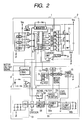
- Fig. 2 is a motor drive control circuit block diagram concretely showing a block of a motor drive control system shown in Fig. 1.
- the reference numeral 1 denotes a phase switching timing signal generating portion for generating a phase switching timing signal
- 2 a driver for performing motor 21 drive
- 3 a motor drive control logic portion
- 4 an FG detecting portion for generating a rotational signal in response to the rotation of the motor
- 5 a speed control portion.
- the motor drive control system shown in Fig. 1 is configured by well known techniques.
- One such well known technique involves a motor driver "HA13605" commercially available from Hitachi, Ltd. as one example.
- the speed control portion includes a reference clock generating portion 51 (clock generator 51), a divider 52 which divides a reference clock from the reference clock generating portion, a noise filter 53, a discremeter 54, a speed monitor 55, and a charging/discharging circuit 56.
- the discremeter 54 compares a clock from the clock generator 51, divided with the divider 52, with a rotational signal from the FG detecting portion through the noise filter 53.
- the charging/discharging circuit 56 consists of a charge pump 56a, a clamp circuit 56b, resistance, and a capacitance. When the charging/discharging circuit 56 has no speed above a desired speed, it is charged to increase the voltage, on the other hand, when the charging/discharging circuit 56 has a speed above a desired speed, it is discharged to decrease the voltage.
- This voltage generates a level signal which determines the pulse width of the PWM clock pulse signal which will be described later.
- a motor ready signal is output.
- the reference numeral 7 denotes a phase switching logic portion in the phase switching timing signal generating portion 1, and 8 an output buffer of a hole amplifier.
- the reference numeral 6 denotes a PWM frequency generating portion.
- the reference numeral 9 denotes a PLL circuit that is a first PWM frequency generating circuit. This PLL circuit 9 generates the first PWM clock having constant times the phase switching timing signal based on the phase switching timing signal generated by the phase switching timing signal generating portion 1.
- the reference numeral 10 denotes a second PWM frequency generating circuit which generates a second PWM clock.
- the reference numeral 11 is a switching circuit, which switches the second PWM clock generated by the second PWM frequency generating circuit 10 to the first PWM clock generated by the PLL circuit 9, which is the first PWM frequency generating circuit, in response to the rotational speed of the motor, detected by the speed control portion 5.
- the reference numeral 12 denotes a chopping wave generating circuit which shapes a PWM frequency from the switching circuit 11 to a triangular wave.
- the reference numeral 13 denotes a pulse width control portion which can vary the drive pulse width, for controlling the rotational signal of the motor in response to the level signal from the speed control portion 5.
- the second PWM clock generated by the second PWM frequency generating circuit 10 through the switching circuit 11 is supplied to the driver 2 through the pulse width control portion 13.
- the driver 2 switches phases in response to a phase switching timing signal from the phase switching timing signal generating portion 1 to drive the motor 21, in response to the second PWM clock generated by the PWM signal generating portion 104.
- this motor drive is output a rotational signal through the noise filter 53.
- This rotational signal is compared with a value divided with the divider 52, with the discremeter 54.
- a desired speed can be obtained. If it is found by the above comparison that a desired speed is not obtained, the charging/discharging circuit 56 is charged to increase the voltage. This voltage becomes a level signal which determines the pulse width of a second PWM clock signal.
- a chopping wave is generated by the chopping wave generating circuit 12 and the second PWM clock can be varied by this chopping wave and the level signal of the charging/discharging circuit 56 so that the drive pulse width is increased in the pulse width control portion 13.
- the pulse width of the second PWM clock signal is increased, whereby driving of the motor 21 allows the speed of the motor 21 to increase. Accordingly, when the motor speed reaches the desired one, a motor ready signal is output from a speed monitor 55.
- the switching circuit 11 is switched from the second PWM clock to the first PWM clock generated from the PLL circuit 9 which is the first PWM signal generating means, by receiving the motor ready signal.
- the first PWM clock generated from the PLL circuit 9 is applied to the driver 2 through the switching circuit 11, and the driver 2 is phase-switched by a phase switching timing signal from the phase switching timing signal generating portion 1. Then driving of the motor 21 is performed in response to the first PWM clock generated by the PLL circuit 9.
- the PLL circuit 9 since the PLL circuit 9 generates a first PWM clock which is a constant-fold overage the phase switching timing signal in response to the phase switching timing signal generated by the phase switching timing signal generating portion 1, the first PWM clock is synchronized with the phase switching timing signal. For example, when a frequency is varied to six-fold, the motor drive pulse of each phase becomes six pulses equally.
- the second PWM clock is controlled by a frequency generated by the second PWM frequency generating circuit 10.
- the frequency is switched to the PWM frequency generated by use of the motor ready signal from the speed control portion 5.
- the wave in this PWM frequency is shaped to a chopping wave by use of the PWM-controlled chopping wave generating circuit 12.
- Fig. 7 shows a non-synchronous state before being switched to the PWM frequency by use of the switching circuit. Even if the same drive pulse is applied to each phase, since the PWM clock timing is different from the switching timing of each phase, integrated values of the respective phase pulses are differentiated from each other. As the result, since the number of pulses becomes small for the drive time of each phase of the motor rotating at a high speed and small rotational torque of the motor has driving force differences, rotational irregularities of the motor occur due to the integrated value differences.
- the PWM frequency After switching of the PWM frequency, which is a characteristic of the present invention, the PWM frequency has a relation of constant-fold over the phase switching timing, as shown in Fig. 3. Therefore, the numbers of the PWM drive pulses of the respective phases become the same and the time from the switching timing until the first drive pulse can be identified at each phase.
- the integrated values of the pulses of the phases are equalized. Accordingly, the accuracy of the rotational speed control of the motor and the stability of the motor can be enhanced.
- synchronization of the PWM clock with the phase switching timing is obtained by the reference clock signal from the reference clock generating portion and an FG signal, which is a rotational signal from the FG detecting portion, based on the motor rotation.
- Fig. 5 is a motor drive control circuit block diagram concretely showing a block of a motor drive control system in Fig. 1.
- the same elements as in the first embodiment are denoted by the same references as therein and concrete descriptions are omitted.
- the differences between the first embodiment and second embodiment resides in a PWM frequency generating portion 14.
- a reference clock generated by a reference clock generating portion 51 is divided to be PWM clocks.
- the PWM clocks are shaped to chopping waves by a chopping wave generating circuit 16 and transmitted to a pulse width control portion 17.
- the motor rotational control is performed so that the reference clock is synchronized with an FG signal which is a detecting signal for the rotation of the motor.
- the FG signal ffg is n (integer)-fold over the number of revolutions of the motor.
- the phase switched number per revolution of the motor corresponds to a number N of one phase per revolution of the motor.
- the PWM frequency fqwm has a relation to the reference clock fosc.
- the drive timing of each phase can be synchronized with the PWM frequency, whereby a PWM frequency synchronized with the phase switching timing can be generated from the reference clock by only use of the divider.
- the cost up and complicatedness of circuits can be prevented, and also, the rotational irregularities of the motor can be decreased as in embodiment 1. Further, the rotational accuracy and stability can be enhanced.
- the PWM clock divided with the divider 15 is supplied to the driver 2 through the chopping wave generating circuit 16 and the pulse width control portion 17.
- the driver 2 switches phases in response to a phase switching timing signal from the phase switching timing signal generating portion 1 to drive the motor 21, in response to the PWM clock divided with the divider 16.
- this motor drive is output a rotational signal through the noise filter 53.
- This rotational signal is compared with a value divided with the divider 52, with the discremeter 54. If it is found by the above comparison that a desired speed is not obtained, the charging/discharging circuit 56 is charged to increase the voltage.
- This voltage becomes a level signal which determines the pulse width of a PWM clock signal.
- a chopping wave is generated by the chopping wave generating circuit 16 and the PWM clock can be varied by this chopping wave and the level signal of the charging/discharging circuit 56 so that the drive pulse width is increased in the pulse width control portion 17.
- the pulse width of the PWM clock signal is increased, whereby driving of the motor 21 allows the speed of the motor 21 to increase. Accordingly, when the motor speed reaches the desired one, that is, when the clock pulse is equalized with one pulse of the rotational signal, the drive pulse width becomes a constant width through the pulse width control portion 17.
- the PWM clock having a constant drive pulse width is applied to the driver 2 through the switching circuit 11, and the driver 2 is phase-switched by a phase switching timing signal from the phase switching timing signal generating portion 1. Then driving of the motor 21 is performed in response to the PWM clock having the constant drive pulse width.
- the drive switching timing of each phase and the PWM drive frequency are synchronized to each other, and the PWM pulse number of each phase is equalized to each other. Further, the time from the phase switching timing until the first pulse can be also equalized to each other.
- a motor having a large number of revolutions occurs rotational irregularities of the rotation of motor when controlled non-synchronously.
- a large PWM pulse number for switching timing of each phase cannot be used due to the switching speed and loss, the on-time of a non-synchronous pulse of each phase is different from each other and the motor is effected by the pulse deviations whereby rotational irregularities of the motor are increased.
- the motor uses a resistance and a capacitor, variance in frequency which is derived from the irregularities of the device and the change of properties by temperature can be prevented. As the result, while preventing the cost up and the complicatedness of circuits, rotational irregularities of the motor can be decreased and a motor rotational control having a high accuracy can be realized.
- the present invention is effective to perform a high accurate rotational control of a drive motor for an optical disk device having a high rotation of the motor and a polygon drive motor for a laser printer, digital copy machine etc.
Landscapes
- Engineering & Computer Science (AREA)
- Power Engineering (AREA)
- Control Of Motors That Do Not Use Commutators (AREA)
- Control Of Ac Motors In General (AREA)
Abstract
Description
- The present invention relates to a motor drive control system that carry out a motor drive control digitally by use of a PWM (Pulse Width Moduration) drive.
- In a digital speed control using a direct PWM drive of a motor, a PWM drive frequency has been generated by an oscillation circuit e.g., an RC oscillation circuit using a resistance and a capacitor, thereby controlling the digital speed control non-synchronously with each set of switching timing of the motor.
- In such a motor drive control system, however, the PWM drive pulse number of each phase and the time from the switching timing of each phase until the first PWM drive pulse are different from each other and deviation in the driving timing of each phase has occurred. As the result, rotational irregularity has occurred particularly, when a large PWM pulse number cannot be used for the switching timing of each phase by the stepping speed and loss, in a motor which has a large number of rotations, the on-times of the respective PWM pulses are different from each other as the pulses are non-synchronous with each other, and effects of the above-mentioned timing irregularity are increased whereby the rotational irregularity is also increased. Further, since the system uses the resistance and capacitor, the frequency variance has occurred by the variance of devices or elements and the characteristic variance due to temperature.
- Accordingly, an object of the present invention is to provide a motor drive control system in which the drive switching timing of each phase of the motor and the PWM drive frequency are synchronized with each other.
- Another object of the present invention is to provide a motor drive control system in which PWM drive pulse numbers of the respective phases of motor are identified.
- Other objects of the present invention will become apparent from the detailed embodiments described below.
-
- Fig. 1 is a block diagram showing a basic configuration of a motor drive control system according to the present invention;
- Fig. 2 is a control circuit block diagram according to a first embodiment concretely showing a motor drive control system in Fig. 1;
- Fig. 3 is a signal waveform diagram showing each of control circuit portions shown in Fig. 2;
- Fig. 4 is a circuit diagram showing details of a phase switching logic circuit shown in Fig. 3;
- Fig. 5 is a control circuit block diagram according to a second embodiment concretely showing a basic configuration of a motor drive control system in Fig. 1;
- Fig. 6 is a signal waveform diagram showing each of control circuit portions shown in Fig. 5; and
- Fig. 7 is a signal waveform diagram showing a state where the drive switching timing of each phase of a motor and the PWM drive frequency are synchronous with each other.
-
- Some embodiments of the present invention will be described with reference to drawings hereinbelow.
- Fig. 1 is a block diagram showing a basic configuration of a motor drive control system according to the present invention. In Fig. 1, the
reference numeral 101 denotes a phase switching timing signal generating portion for generating a phase switching timing signal, 102 a driver for performing motor drive, 103 a motor, 104 a PWM signal generating portion for generating a PWM clock, 105 is a synchronizing means for synchronizing a phase switching timing with a PWM clock. - By the above-mentioned configuration, the
driver 102 for performing the motor drive phase-switches by use of the phase switching timing signal from the phase switching timingsignal generating portion 101 and drives themotor 103 in response to the PWM clock generated from the PWMsignal generating portion 104. At this time, the PWM clock generated from the PWMsignal generating portion 104 uses the phase switching timing signal synchronous with the phase switching timing a phase switching timing signal which is synchronized with the phase switching timing by thesynchronizing means 105. - A first embodiment concretely showing the block of the motor drive control system shown in Fig. 1 will now be described with reference to Figs. 2 to 4 herein below.
- Fig. 2 is a motor drive control circuit block diagram concretely showing a block of a motor drive control system shown in Fig. 1. In Fig. 2, the
reference numeral 1 denotes a phase switching timing signal generating portion for generating a phase switching timing signal, 2 a driver for performingmotor 21 drive, 3 a motor drive control logic portion, 4 an FG detecting portion for generating a rotational signal in response to the rotation of the motor, and 5 a speed control portion. The motor drive control system shown in Fig. 1 is configured by well known techniques. One such well known technique involves a motor driver "HA13605" commercially available from Hitachi, Ltd. as one example. - The speed control portion includes a reference clock generating portion 51 (clock generator 51), a
divider 52 which divides a reference clock from the reference clock generating portion, anoise filter 53, adiscremeter 54, aspeed monitor 55, and a charging/discharging circuit 56. Thediscremeter 54 compares a clock from theclock generator 51, divided with thedivider 52, with a rotational signal from the FG detecting portion through thenoise filter 53. The charging/discharging circuit 56 consists of acharge pump 56a, aclamp circuit 56b, resistance, and a capacitance. When the charging/discharging circuit 56 has no speed above a desired speed, it is charged to increase the voltage, on the other hand, when the charging/discharging circuit 56 has a speed above a desired speed, it is discharged to decrease the voltage. - This voltage generates a level signal which determines the pulse width of the PWM clock pulse signal which will be described later. At a predetermined speed, a motor ready signal is output.
- The
reference numeral 7 denotes a phase switching logic portion in the phase switching timingsignal generating portion reference numeral 6 denotes a PWM frequency generating portion. In this PWMfrequency generating portion 6, the reference numeral 9 denotes a PLL circuit that is a first PWM frequency generating circuit. This PLL circuit 9 generates the first PWM clock having constant times the phase switching timing signal based on the phase switching timing signal generated by the phase switching timingsignal generating portion 1. Thereference numeral 10 denotes a second PWM frequency generating circuit which generates a second PWM clock. Thereference numeral 11 is a switching circuit, which switches the second PWM clock generated by the second PWMfrequency generating circuit 10 to the first PWM clock generated by the PLL circuit 9, which is the first PWM frequency generating circuit, in response to the rotational speed of the motor, detected by thespeed control portion 5. Thereference numeral 12 denotes a chopping wave generating circuit which shapes a PWM frequency from theswitching circuit 11 to a triangular wave. Thereference numeral 13 denotes a pulse width control portion which can vary the drive pulse width, for controlling the rotational signal of the motor in response to the level signal from thespeed control portion 5. - Thus, in the first stage after the start of a rotational drive of the motor, the second PWM clock generated by the second PWM
frequency generating circuit 10 through theswitching circuit 11 is supplied to thedriver 2 through the pulsewidth control portion 13. Thedriver 2 switches phases in response to a phase switching timing signal from the phase switching timingsignal generating portion 1 to drive themotor 21, in response to the second PWM clock generated by the PWMsignal generating portion 104. - By this motor drive is output a rotational signal through the
noise filter 53. This rotational signal is compared with a value divided with thedivider 52, with thediscremeter 54. For example, in the above-mentioned motor driver HA13605 of Hitachi, Ltd., when the 2048 clock is the same as arotational signal 1 pulse, a desired speed can be obtained. If it is found by the above comparison that a desired speed is not obtained, the charging/discharging circuit 56 is charged to increase the voltage. This voltage becomes a level signal which determines the pulse width of a second PWM clock signal. In the second PWM clock of the second PWMfrequency generating circuit 10, a chopping wave is generated by the choppingwave generating circuit 12 and the second PWM clock can be varied by this chopping wave and the level signal of the charging/discharging circuit 56 so that the drive pulse width is increased in the pulsewidth control portion 13. As the result, the pulse width of the second PWM clock signal is increased, whereby driving of themotor 21 allows the speed of themotor 21 to increase. Accordingly, when the motor speed reaches the desired one, a motor ready signal is output from aspeed monitor 55. Theswitching circuit 11 is switched from the second PWM clock to the first PWM clock generated from the PLL circuit 9 which is the first PWM signal generating means, by receiving the motor ready signal. Thus, the first PWM clock generated from the PLL circuit 9 is applied to thedriver 2 through theswitching circuit 11, and thedriver 2 is phase-switched by a phase switching timing signal from the phase switching timingsignal generating portion 1. Then driving of themotor 21 is performed in response to the first PWM clock generated by the PLL circuit 9. In this case, since the PLL circuit 9 generates a first PWM clock which is a constant-fold overage the phase switching timing signal in response to the phase switching timing signal generated by the phase switching timingsignal generating portion 1, the first PWM clock is synchronized with the phase switching timing signal. For example, when a frequency is varied to six-fold, the motor drive pulse of each phase becomes six pulses equally. - Therefore, in the first stage after the start of the rotational drive of the motor, the second PWM clock is controlled by a frequency generated by the second PWM
frequency generating circuit 10. When a desired number of revolutions of the motor is obtained by use of the frequency generated by the second PWMfrequency generating circuit 10, the frequency is switched to the PWM frequency generated by use of the motor ready signal from thespeed control portion 5. The wave in this PWM frequency is shaped to a chopping wave by use of the PWM-controlled choppingwave generating circuit 12. As the result, the drive pulse width of the second PWM clock signal can be varied by a level signal generated by thespeed control portion 5 and the rotational speed control of the motor can be performed. - Fig. 7 shows a non-synchronous state before being switched to the PWM frequency by use of the switching circuit. Even if the same drive pulse is applied to each phase, since the PWM clock timing is different from the switching timing of each phase, integrated values of the respective phase pulses are differentiated from each other. As the result, since the number of pulses becomes small for the drive time of each phase of the motor rotating at a high speed and small rotational torque of the motor has driving force differences, rotational irregularities of the motor occur due to the integrated value differences.
- After switching of the PWM frequency, which is a characteristic of the present invention, the PWM frequency has a relation of constant-fold over the phase switching timing, as shown in Fig. 3. Therefore, the numbers of the PWM drive pulses of the respective phases become the same and the time from the switching timing until the first drive pulse can be identified at each phase. When the same drive pulse is applied to each of phases, the integrated values of the pulses of the phases are equalized. Accordingly, the accuracy of the rotational speed control of the motor and the stability of the motor can be enhanced.
- A second embodiment concretely showing the block of the motor drive control system of Fig. 1 will now be described with reference to Figs. 5 and 6.
- In this second embodiment, synchronization of the PWM clock with the phase switching timing is obtained by the reference clock signal from the reference clock generating portion and an FG signal, which is a rotational signal from the FG detecting portion, based on the motor rotation.
- Fig. 5 is a motor drive control circuit block diagram concretely showing a block of a motor drive control system in Fig. 1. In Fig. 5, the same elements as in the first embodiment are denoted by the same references as therein and concrete descriptions are omitted. The differences between the first embodiment and second embodiment resides in a PWM
frequency generating portion 14. In this PWMfrequency generating portion 14, a reference clock generated by a referenceclock generating portion 51 is divided to be PWM clocks. The PWM clocks are shaped to chopping waves by a choppingwave generating circuit 16 and transmitted to a pulsewidth control portion 17. - The motor rotational control is performed so that the reference clock is synchronized with an FG signal which is a detecting signal for the rotation of the motor. The reference clock fosc has a relation between the FG signal ffg, the divisional number divided with a
divider 5, and the counted number counted with adiscremeter 54. The relation is expressed by a function that is, fosc = d × c × ffg. In this case, the FG signal ffg is n (integer)-fold over the number of revolutions of the motor. Further, the phase switched number per revolution of the motor corresponds to a number N of one phase per revolution of the motor. In this case, the PWM frequency fqwm has a relation to the reference clock fosc. The relation is expressed by a function that is, fqwm = fosc/D, where D is a divisional number in thedivider 15 for the PWMfrequency generating portion 14. - Therefore, the following function that is, fqwm = [(d × c)/D] × ffg, is obtained. In the relation between the FG signal and the phase switching, the number of switching per revolution is expressed by N/n. Thus, if a function, [(d × c)/D] × N/n is set to be an integer, the PWM frequency can be synchronized with the phase switching timing.
- Therefore, if this relation is satisfied, the drive timing of each phase can be synchronized with the PWM frequency, whereby a PWM frequency synchronized with the phase switching timing can be generated from the reference clock by only use of the divider. As the result, the cost up and complicatedness of circuits can be prevented, and also, the rotational irregularities of the motor can be decreased as in
embodiment 1. Further, the rotational accuracy and stability can be enhanced. - Thus, in the first stage after the start of a rotational drive of the motor, the PWM clock divided with the
divider 15 is supplied to thedriver 2 through the choppingwave generating circuit 16 and the pulsewidth control portion 17. Thedriver 2 switches phases in response to a phase switching timing signal from the phase switching timingsignal generating portion 1 to drive themotor 21, in response to the PWM clock divided with thedivider 16. - By this motor drive is output a rotational signal through the
noise filter 53. This rotational signal is compared with a value divided with thedivider 52, with thediscremeter 54. If it is found by the above comparison that a desired speed is not obtained, the charging/dischargingcircuit 56 is charged to increase the voltage. This voltage becomes a level signal which determines the pulse width of a PWM clock signal. In the PWM clock, a chopping wave is generated by the choppingwave generating circuit 16 and the PWM clock can be varied by this chopping wave and the level signal of the charging/dischargingcircuit 56 so that the drive pulse width is increased in the pulsewidth control portion 17. As the result, the pulse width of the PWM clock signal is increased, whereby driving of themotor 21 allows the speed of themotor 21 to increase. Accordingly, when the motor speed reaches the desired one, that is, when the clock pulse is equalized with one pulse of the rotational signal, the drive pulse width becomes a constant width through the pulsewidth control portion 17. The PWM clock having a constant drive pulse width is applied to thedriver 2 through the switchingcircuit 11, and thedriver 2 is phase-switched by a phase switching timing signal from the phase switching timingsignal generating portion 1. Then driving of themotor 21 is performed in response to the PWM clock having the constant drive pulse width. - As described above, according to the present invention, the drive switching timing of each phase and the PWM drive frequency are synchronized to each other, and the PWM pulse number of each phase is equalized to each other. Further, the time from the phase switching timing until the first pulse can be also equalized to each other.
- Therefore, a motor having a large number of revolutions occurs rotational irregularities of the rotation of motor when controlled non-synchronously. Further, when a large PWM pulse number for switching timing of each phase cannot be used due to the switching speed and loss, the on-time of a non-synchronous pulse of each phase is different from each other and the motor is effected by the pulse deviations whereby rotational irregularities of the motor are increased. Furthermore, since the motor uses a resistance and a capacitor, variance in frequency which is derived from the irregularities of the device and the change of properties by temperature can be prevented. As the result, while preventing the cost up and the complicatedness of circuits, rotational irregularities of the motor can be decreased and a motor rotational control having a high accuracy can be realized.
- The present invention is effective to perform a high accurate rotational control of a drive motor for an optical disk device having a high rotation of the motor and a polygon drive motor for a laser printer, digital copy machine etc.
Claims (8)
- A drive control system for a motor (21,103) comprising a drive means (2, 102) for performing phase switching by use of a phase switching timing signal from a phase switching timing generating means (1, 101) and driving of said motor (21, 103) in response to a PWM clock generated from a PWM signal generating means (6, 104), characterized by providing a synchronizing means (5, 15, 9, 105) for synchronizing the PWM clock of said PWM signal generating means (6, 14, 104) with said phase switching timing.
- A motor drive control system according to claim 1, wherein said synchronizing means generates a PWM clock which is a constant-fold over the phase switching timing signal from said PWM signal generating means (6, 104) in response to the phase timing signal generated by said phase switching timing generating means (1, 101).
- A motor drive control system according to claim 1, further comprising:a reference clock signal generating means (51) for generating a reference clock signal;a detecting means (4) for detecting a rotational speed of the motor and generating a rotational signal in response to said rotational speed;wherein said synchronizing means generates a PWM clock frequency synchronized with a phase switching timing from said PWM signal generating means (14) by use of the reference clock signal from said reference clock signal generating means and the rotational signal from said detecting means.
- A motor drive control system according to claim 3, wherein when said reference clock signal is defined as fosc, a divisional number for dividing the reference clock signal is defined as D, a divisional number for dividing the rotational signal ffg from said detecting means is defined as d, and a count with discremeter (54) is defined as c, an equation fosc = d × c × ffg is satisfied, and when a number of the detecting means for one revolution of the motor is defined as n and a number of one phase per revolution of the motor is defined as N, a function [(d × c)/D] × (N/n) is an integer.
- A motor drive control system according to any preceding claim, further comprising:a detecting means (4) for detecting a rotational speed of the motor; anda drive pulse width varying means (13, 17) for varying the drive pulse width of said PWM clock to control the rotational speed of the motor, in response to the rotational speed of the motor, detected with said detecting means.
- A motor drive control system according to claim 2, further comprising:a second PWM signal generating means (10) for generating a second PWM clock;a detecting means (4) for detecting a rotational speed of the motor; anda switching means (11) for switching the second PWM clock generated with said second PWM signal generating means to a PWM clock which is a constant-fold over said second PWM clock, generated with said PWM signal generating means, in response to the rotational speed of the motor, detected with said detecting means.
- A method of driving a motor comprising providing a phase switching timing signal from a phase switching timing signal generating means;performing phase switching using said phase switching timing signal;providing a pulse width modulation clock signal from a pulse width modulation signal generating means; and synchronising the pulse width modulation clock signal with said phase switching timing signal.
- A data carrier carrying processor-implementable instructions for carrying out the method of claim 7.
Applications Claiming Priority (2)
| Application Number | Priority Date | Filing Date | Title |
|---|---|---|---|
| JP36524797 | 1997-12-19 | ||
| JP36524797 | 1997-12-19 |
Publications (3)
| Publication Number | Publication Date |
|---|---|
| EP0929144A2 true EP0929144A2 (en) | 1999-07-14 |
| EP0929144A3 EP0929144A3 (en) | 2000-04-12 |
| EP0929144B1 EP0929144B1 (en) | 2006-04-26 |
Family
ID=18483793
Family Applications (1)
| Application Number | Title | Priority Date | Filing Date |
|---|---|---|---|
| EP98310465A Expired - Lifetime EP0929144B1 (en) | 1997-12-19 | 1998-12-18 | Motor drive control system and method |
Country Status (3)
| Country | Link |
|---|---|
| US (1) | US6054820A (en) |
| EP (1) | EP0929144B1 (en) |
| DE (1) | DE69834312T2 (en) |
Families Citing this family (1)
| Publication number | Priority date | Publication date | Assignee | Title |
|---|---|---|---|---|
| JP2004242432A (en) * | 2003-02-06 | 2004-08-26 | Canon Inc | Direct-current motor drive |
Citations (6)
| Publication number | Priority date | Publication date | Assignee | Title |
|---|---|---|---|---|
| US4791345A (en) * | 1986-08-20 | 1988-12-13 | Lgz Landis & Gyr Zug Ag | Driving device for a stepping motor |
| US5485070A (en) * | 1992-09-29 | 1996-01-16 | Canon Kabushiki Kaisha | Stepping-motor driving system |
| JPH0823694A (en) * | 1994-07-07 | 1996-01-23 | Hitachi Ltd | Sped control device of dc brushless motor |
| JPH0847284A (en) * | 1994-07-29 | 1996-02-16 | Matsushita Electric Ind Co Ltd | Drive device of brushless motor |
| EP0712253A2 (en) * | 1994-11-14 | 1996-05-15 | Texas Instruments Incorporated | Improvements in or relating to image display systems |
| US5677605A (en) * | 1989-08-22 | 1997-10-14 | Unique Mobility, Inc. | Brushless DC motor using phase timing advancement |
Family Cites Families (5)
| Publication number | Priority date | Publication date | Assignee | Title |
|---|---|---|---|---|
| DE3268669D1 (en) * | 1981-08-03 | 1986-03-06 | Hitachi Ltd | Apparatus for driving a polyphase brushless motor with a suppressed torque ripple |
| US4546293A (en) * | 1982-08-24 | 1985-10-08 | Sundstrand Corporation | Motor control for a brushless DC motor |
| US4608527A (en) * | 1982-12-20 | 1986-08-26 | Sundstrand Corporation | Phase advance waveform generator for brushless DC actuator system controller |
| JPH0471386A (en) * | 1990-07-09 | 1992-03-05 | Yamamoto Denki Kk | Controller for synchronous motor |
| US5448141A (en) * | 1994-03-18 | 1995-09-05 | North Carolina State University | Adjustable speed drive for residential applications |
-
1998
- 1998-12-17 US US09/213,862 patent/US6054820A/en not_active Expired - Fee Related
- 1998-12-18 EP EP98310465A patent/EP0929144B1/en not_active Expired - Lifetime
- 1998-12-18 DE DE69834312T patent/DE69834312T2/en not_active Expired - Lifetime
Patent Citations (6)
| Publication number | Priority date | Publication date | Assignee | Title |
|---|---|---|---|---|
| US4791345A (en) * | 1986-08-20 | 1988-12-13 | Lgz Landis & Gyr Zug Ag | Driving device for a stepping motor |
| US5677605A (en) * | 1989-08-22 | 1997-10-14 | Unique Mobility, Inc. | Brushless DC motor using phase timing advancement |
| US5485070A (en) * | 1992-09-29 | 1996-01-16 | Canon Kabushiki Kaisha | Stepping-motor driving system |
| JPH0823694A (en) * | 1994-07-07 | 1996-01-23 | Hitachi Ltd | Sped control device of dc brushless motor |
| JPH0847284A (en) * | 1994-07-29 | 1996-02-16 | Matsushita Electric Ind Co Ltd | Drive device of brushless motor |
| EP0712253A2 (en) * | 1994-11-14 | 1996-05-15 | Texas Instruments Incorporated | Improvements in or relating to image display systems |
Non-Patent Citations (2)
| Title |
|---|
| PATENT ABSTRACTS OF JAPAN vol. 1996, no. 05, 31 May 1996 (1996-05-31) & JP 08 023694 A (HITACHI LTD), 23 January 1996 (1996-01-23) * |
| PATENT ABSTRACTS OF JAPAN vol. 1996, no. 06, 28 June 1996 (1996-06-28) & JP 08 047284 A (MATSUSHITA ELECTRIC IND CO LTD;OTHERS: 01), 16 February 1996 (1996-02-16) * |
Also Published As
| Publication number | Publication date |
|---|---|
| EP0929144B1 (en) | 2006-04-26 |
| US6054820A (en) | 2000-04-25 |
| DE69834312T2 (en) | 2007-01-11 |
| DE69834312D1 (en) | 2006-06-01 |
| EP0929144A3 (en) | 2000-04-12 |
Similar Documents
| Publication | Publication Date | Title |
|---|---|---|
| EP0589630B1 (en) | Automatic adjustment of commutation delay for brushless DC motor | |
| US5223772A (en) | Method and apparatus for providing the lock of a phase-locked loop system from frequency sweep | |
| US5612598A (en) | Vibration driven motor | |
| KR0154854B1 (en) | Sensorless dc brushless motor start-up circuit using unbalancing clock | |
| US6196650B1 (en) | Sensorless motor driving circuit having a comparative phase lock loop arrangement | |
| JPS5981712A (en) | Control system | |
| EP0259089B1 (en) | Drive apparatus | |
| JPH07112360B2 (en) | Control method and apparatus for PWM inverter | |
| US6111372A (en) | Sensorless motor driver | |
| EP0929144A2 (en) | Motor drive control system and method | |
| US5661359A (en) | Vibration type motor device | |
| JP3796177B2 (en) | Motor PWM drive circuit | |
| JP3235742B2 (en) | Motor control drive circuit | |
| JP3733255B2 (en) | Motor drive control device | |
| EP0893877B1 (en) | Motor drive system controlled by a phase accumulator and method therefor | |
| CA1111906A (en) | Motor control system | |
| JP2002125388A (en) | Motor driver | |
| US6998799B2 (en) | System and method for improved motor control | |
| US4998053A (en) | Method and apparatus for reducing a current break in a leg that is not participating in the commutation of a three-phase block current fed synchronous machine | |
| JPH0519388B2 (en) | ||
| JP3277728B2 (en) | Speed controller for electric motor | |
| JP2753906B2 (en) | Method and apparatus for driving brushless motor | |
| JP3294644B2 (en) | Motor control device | |
| JPS60125200A (en) | Controller | |
| JP3263200B2 (en) | Synchronous signal generation circuit and frequency division circuit |
Legal Events
| Date | Code | Title | Description |
|---|---|---|---|
| PUAI | Public reference made under article 153(3) epc to a published international application that has entered the european phase |
Free format text: ORIGINAL CODE: 0009012 |
|
| AK | Designated contracting states |
Kind code of ref document: A2 Designated state(s): DE FR GB IT |
|
| AX | Request for extension of the european patent |
Free format text: AL;LT;LV;MK;RO;SI |
|
| PUAL | Search report despatched |
Free format text: ORIGINAL CODE: 0009013 |
|
| AK | Designated contracting states |
Kind code of ref document: A3 Designated state(s): AT BE CH CY DE DK ES FI FR GB GR IE IT LI LU MC NL PT SE |
|
| AX | Request for extension of the european patent |
Free format text: AL;LT;LV;MK;RO;SI |
|
| RIC1 | Information provided on ipc code assigned before grant |
Free format text: 7H 02P 6/06 A, 7H 02P 7/63 B |
|
| 17P | Request for examination filed |
Effective date: 20000824 |
|
| AKX | Designation fees paid |
Free format text: DE FR GB IT |
|
| 17Q | First examination report despatched |
Effective date: 20030731 |
|
| GRAP | Despatch of communication of intention to grant a patent |
Free format text: ORIGINAL CODE: EPIDOSNIGR1 |
|
| GRAS | Grant fee paid |
Free format text: ORIGINAL CODE: EPIDOSNIGR3 |
|
| GRAA | (expected) grant |
Free format text: ORIGINAL CODE: 0009210 |
|
| AK | Designated contracting states |
Kind code of ref document: B1 Designated state(s): DE FR GB IT |
|
| REG | Reference to a national code |
Ref country code: GB Ref legal event code: FG4D |
|
| RIC1 | Information provided on ipc code assigned before grant |
Ipc: H02P 27/08 20060101ALI20060308BHEP Ipc: H02P 6/06 20060101AFI20060308BHEP |
|
| REF | Corresponds to: |
Ref document number: 69834312 Country of ref document: DE Date of ref document: 20060601 Kind code of ref document: P |
|
| ET | Fr: translation filed | ||
| PGFP | Annual fee paid to national office [announced via postgrant information from national office to epo] |
Ref country code: IT Payment date: 20061231 Year of fee payment: 9 |
|
| PLBE | No opposition filed within time limit |
Free format text: ORIGINAL CODE: 0009261 |
|
| STAA | Information on the status of an ep patent application or granted ep patent |
Free format text: STATUS: NO OPPOSITION FILED WITHIN TIME LIMIT |
|
| 26N | No opposition filed |
Effective date: 20070129 |
|
| PGFP | Annual fee paid to national office [announced via postgrant information from national office to epo] |
Ref country code: FR Payment date: 20061218 Year of fee payment: 9 |
|
| REG | Reference to a national code |
Ref country code: FR Ref legal event code: ST Effective date: 20081020 |
|
| PG25 | Lapsed in a contracting state [announced via postgrant information from national office to epo] |
Ref country code: FR Free format text: LAPSE BECAUSE OF NON-PAYMENT OF DUE FEES Effective date: 20071231 |
|
| PG25 | Lapsed in a contracting state [announced via postgrant information from national office to epo] |
Ref country code: IT Free format text: LAPSE BECAUSE OF NON-PAYMENT OF DUE FEES Effective date: 20071218 |
|
| PGFP | Annual fee paid to national office [announced via postgrant information from national office to epo] |
Ref country code: GB Payment date: 20101223 Year of fee payment: 13 |
|
| PGFP | Annual fee paid to national office [announced via postgrant information from national office to epo] |
Ref country code: DE Payment date: 20101231 Year of fee payment: 13 |
|
| GBPC | Gb: european patent ceased through non-payment of renewal fee |
Effective date: 20111218 |
|
| REG | Reference to a national code |
Ref country code: DE Ref legal event code: R119 Ref document number: 69834312 Country of ref document: DE Effective date: 20120703 |
|
| PG25 | Lapsed in a contracting state [announced via postgrant information from national office to epo] |
Ref country code: GB Free format text: LAPSE BECAUSE OF NON-PAYMENT OF DUE FEES Effective date: 20111218 Ref country code: DE Free format text: LAPSE BECAUSE OF NON-PAYMENT OF DUE FEES Effective date: 20120703 |