EP0924770A1 - Image sensor chip, method for manufacturing the same, and image sensor - Google Patents
Image sensor chip, method for manufacturing the same, and image sensor Download PDFInfo
- Publication number
- EP0924770A1 EP0924770A1 EP97915730A EP97915730A EP0924770A1 EP 0924770 A1 EP0924770 A1 EP 0924770A1 EP 97915730 A EP97915730 A EP 97915730A EP 97915730 A EP97915730 A EP 97915730A EP 0924770 A1 EP0924770 A1 EP 0924770A1
- Authority
- EP
- European Patent Office
- Prior art keywords
- image sensor
- output
- photoelectric conversion
- sensor chip
- conversion elements
- Prior art date
- Legal status (The legal status is an assumption and is not a legal conclusion. Google has not performed a legal analysis and makes no representation as to the accuracy of the status listed.)
- Granted
Links
- 238000004519 manufacturing process Methods 0.000 title claims abstract description 9
- 238000000034 method Methods 0.000 title claims description 8
- 239000000758 substrate Substances 0.000 claims abstract description 48
- 230000003321 amplification Effects 0.000 claims abstract description 34
- 238000006243 chemical reaction Methods 0.000 claims abstract description 34
- 238000003199 nucleic acid amplification method Methods 0.000 claims abstract description 34
- 108091008695 photoreceptors Proteins 0.000 claims abstract description 7
- 239000003990 capacitor Substances 0.000 claims description 25
- 239000011521 glass Substances 0.000 claims description 10
- 238000005520 cutting process Methods 0.000 claims description 3
- 239000000470 constituent Substances 0.000 claims description 2
- 238000005286 illumination Methods 0.000 description 6
- 238000010586 diagram Methods 0.000 description 4
- 230000002411 adverse Effects 0.000 description 3
- 230000008901 benefit Effects 0.000 description 3
- 238000003698 laser cutting Methods 0.000 description 3
- PNEYBMLMFCGWSK-UHFFFAOYSA-N Alumina Chemical compound [O-2].[O-2].[O-2].[Al+3].[Al+3] PNEYBMLMFCGWSK-UHFFFAOYSA-N 0.000 description 2
- XUIMIQQOPSSXEZ-UHFFFAOYSA-N Silicon Chemical compound [Si] XUIMIQQOPSSXEZ-UHFFFAOYSA-N 0.000 description 2
- 238000007650 screen-printing Methods 0.000 description 2
- 229910052710 silicon Inorganic materials 0.000 description 2
- 239000010703 silicon Substances 0.000 description 2
- XAGFODPZIPBFFR-UHFFFAOYSA-N aluminium Chemical compound [Al] XAGFODPZIPBFFR-UHFFFAOYSA-N 0.000 description 1
- 229910052782 aluminium Inorganic materials 0.000 description 1
- 230000006866 deterioration Effects 0.000 description 1
- 230000000694 effects Effects 0.000 description 1
- PCHJSUWPFVWCPO-UHFFFAOYSA-N gold Chemical compound [Au] PCHJSUWPFVWCPO-UHFFFAOYSA-N 0.000 description 1
- 239000010931 gold Substances 0.000 description 1
- 229910052737 gold Inorganic materials 0.000 description 1
- 239000000463 material Substances 0.000 description 1
- 238000012544 monitoring process Methods 0.000 description 1
- 230000002265 prevention Effects 0.000 description 1
- 239000011347 resin Substances 0.000 description 1
- 229920005989 resin Polymers 0.000 description 1
- 230000000717 retained effect Effects 0.000 description 1
Images



Classifications
-
- H—ELECTRICITY
- H10—SEMICONDUCTOR DEVICES; ELECTRIC SOLID-STATE DEVICES NOT OTHERWISE PROVIDED FOR
- H10F—INORGANIC SEMICONDUCTOR DEVICES SENSITIVE TO INFRARED RADIATION, LIGHT, ELECTROMAGNETIC RADIATION OF SHORTER WAVELENGTH OR CORPUSCULAR RADIATION
- H10F99/00—Subject matter not provided for in other groups of this subclass
-
- H—ELECTRICITY
- H04—ELECTRIC COMMUNICATION TECHNIQUE
- H04N—PICTORIAL COMMUNICATION, e.g. TELEVISION
- H04N25/00—Circuitry of solid-state image sensors [SSIS]; Control thereof
- H04N25/60—Noise processing, e.g. detecting, correcting, reducing or removing noise
- H04N25/617—Noise processing, e.g. detecting, correcting, reducing or removing noise for reducing electromagnetic interference, e.g. clocking noise
-
- H—ELECTRICITY
- H04—ELECTRIC COMMUNICATION TECHNIQUE
- H04N—PICTORIAL COMMUNICATION, e.g. TELEVISION
- H04N25/00—Circuitry of solid-state image sensors [SSIS]; Control thereof
- H04N25/70—SSIS architectures; Circuits associated therewith
- H04N25/701—Line sensors
-
- H—ELECTRICITY
- H04—ELECTRIC COMMUNICATION TECHNIQUE
- H04N—PICTORIAL COMMUNICATION, e.g. TELEVISION
- H04N25/00—Circuitry of solid-state image sensors [SSIS]; Control thereof
- H04N25/70—SSIS architectures; Circuits associated therewith
- H04N25/76—Addressed sensors, e.g. MOS or CMOS sensors
- H04N25/78—Readout circuits for addressed sensors, e.g. output amplifiers or A/D converters
-
- H—ELECTRICITY
- H04—ELECTRIC COMMUNICATION TECHNIQUE
- H04N—PICTORIAL COMMUNICATION, e.g. TELEVISION
- H04N25/00—Circuitry of solid-state image sensors [SSIS]; Control thereof
- H04N25/70—SSIS architectures; Circuits associated therewith
- H04N25/76—Addressed sensors, e.g. MOS or CMOS sensors
Definitions
- the present invention relates to an image sensor chip, and to a manufacturing method and image sensor therefor.
- Fig. 11 shows the general structure of a conventional image sensor 10 used in image-scanning devices or in the image read units of fax machines.
- a plurality of image sensor chips 13 are secured within an area whose length corresponds to the read width on a substrate 12 disposed on the bottom surface of a case 11 made of a resin or the like.
- a transparent glass cover 14 is placed on the top surface of the case 11, and a rod lens array 15 for converging a contrast image, which is aligned with a read line L marked on the glass cover 14, as an erect image of the same size on the image sensor chip array is disposed between the read line L and the image sensor chips 13.
- a plurality of LEDs 16, which serve as light sources for illuminating a document D through the back surface of the glass cover 14, are mounted on the a substrate 17 inside the case 11.
- a 1728-bit photoreceptor must be provided to obtain such an image sensor in order to read an A4 document at 8 pixels per millimeter, and 18 image sensor chips 13 should be mounted on the substrate 12 in order to provide, for example, a single image sensor chip with a 96-bit photoreceptor.
- the length of a single image sensor chip 13 is about 12 mm.
- An image sensor chip 13 is fabricated by integrating a plurality of phototransistors that correspond to the photoreceptors, analog switches connected in series with each of the phototransistors, shift registers for sequentially selecting and switching on the analog switches in accordance with clock pulses, and the like. The output side of each of the analog switches is brought out to the output terminal of the chip.
- the analog switches are sequentially switched on, for example, during the fall cycles of clock pulses, with the result that microcurrent analog data corresponding to the amount of light received by each phototransistor are serially outputted to the output terminal of the chip.
- the output terminal of the chip is connected to a load resistor on the substrate, and the potential difference at a terminal of this load resistor is amplified by an amplification circuit mounted on the substrate.
- a first drawback is that the analog data signals outputted from such image sensor chips are microsignals in the form of a high-impedance output, which, basically, facilitates noise pickup and thus impairs the read performance of the image sensor.
- clock pulse signals of several hundred kilohertz for use in data shifting are inputted to the substrate 12 on which the image sensor chips 13 are mounted, and these clock pulse signals are thus ultimately superposed as alternating-current components on the analog data signals (as shown in Fig. 12), adversely affecting the output characteristics.
- Another drawback is that the ICs, capacitors, and resistors constituting the amplification circuit; the varistors for adjusting the gain of the amplification circuit; and a plurality of other electronic components must be mounted on the substrate separately from the image sensor chips, complicating the steps involved in the manufacture of the image sensor substrate. Specifically, the various electronic component themselves are expensive, equipment is needed for mounting these electronic components on the substrate, and the varistors must be individually adjusted while the output of the amplification circuit is measured in order to adjust the gain of the amplification circuit in accordance with the specification requirements of the customer.
- an object of the present invention to provide an image sensor chip for use in constructing a contact-type image sensor such that the substrate on which these components are mounted can be fabricated very easily, and to provide a smaller and thinner image sensor in which the substrate does not require noise prevention and in which a substrate wired on only one side can be used.
- an image sensor chip manufactured by integrating a prescribed number of photoelectric conversion elements as photoreceptors, analog switches connected in series to the corresponding photoelectric conversion elements, and a switch circuit for sequentially switching on the analog switches in accordance with clock signals; wherein this image sensor chip is characterized by further comprising
- the image sensor chip comprises a power terminal, a ground terminal, a clock signal input terminal, an analog signal output terminal, photoelectric conversion elements arranged in a row at regular intervals and connected at one end to the power terminal, analog switches connected to the respective output terminals of the photoelectric conversion elements, a switch circuit for sequentially switching on the analog switches in accordance with clock signals, and output load components jointly interposed between the ground terminal and the output terminals of the analog switches, wherein the chip is configured such that the output of the amplification circuit is outputted to the analog signal output terminal.
- the output load is a load resistor.
- the output load is a load capacitor.
- the output load consists of a load resistor and a load capacitor connected in parallel to each other.
- the gain-adjusting resistor of the amplification circuit is also fabricated in integral form, and the gain-adjusting resistor comprises a plurality of resistors connected in series and cuttable bypass wirings provided to all or some of the plurality of resistors.
- the amplification circuit is an operational amplifier; that the gain-adjusting resistor comprises a resistor group interposed between the inverting input and the output of the operational amplifier, and a resistor group interposed between the ground and the inverting input of the operational amplifier; and that each resistor group comprises a plurality of resistors connected in series and cuttable bypass wirings provided to all or some of these resistors.
- the image sensor chip pertaining to the subject invention is fabricated by integrating output load components for photoelectric conversion elements, and an amplification circuit for amplifying a terminal potential of these output load components into a single chip in addition to the basic structure of the image sensor chip comprising a prescribed number of photoelectric conversion elements serving as photoreceptors, analog switches connected in series to the corresponding photoelectric conversion elements, a switch circuit for sequentially switching on the analog switches in accordance with clock signals, and the like.
- a resistor for adjusting the gain of the amplification circuit is also integrated into the chip.
- the microcurrent signals outputted as image read signals from the photoelectric conversion elements are outputted (without being allowed to escape from the sensor chips) outside as analog voltage signals obtained by amplifying with an amplification circuit the potential of the output load components on the side of the photoelectric conversion elements. It is therefore possible to markedly reduce or completely prevent the conventionally observed undesirable deterioration in the image read performance due to noise induced by clock signals. As a result, there is no need to provide the substrate for mounting such image sensor chips with amplification circuits or related components, or to form special wiring patterns for noise reduction, making it possible to position the image sensor chips on one side of the substrate and to provide a power source in order to complete the image sensors.
- a substrate obtained by mounting image sensor chips and light-emitting elements (light sources) on one side in such a manner is attached to the bottom surface of a case, a glass cover is placed on the top surface of the case, and an image sensor is configured such that reflected light from a document on the glass cover illuminated by the light-emitting elements is converged on the photoelectric conversion elements of the image sensor chips, in which case the back surface of the substrate facing the reverse side of this image sensor is free from the irregularities caused by the presence of electronic components, resulting in an improved outward appearance.
- the thickness dimensions of the image sensor itself can thereby be further reduced, and a narrower space is sufficient for accommodating the image sensor in an instrument designed for use with such image sensors.
- An advantage of using a resistance load as the output load of the amplification circuit is that the desired analog output waveform can be obtained by selecting an appropriate resistance for the load.
- the analog output waveform should resemble a rectangular wave, that is, should have a horizontal or roughly horizontal top portion, to achieve accurate sensing of the output level, and the desirable output waveform can be obtained by appropriately selecting the resistance value of the resistance load.
- the combined benefits of using a resistance load and a load capacitor can be obtained when these resistance load and load capacitor are connected in parallel with each other as the output load components of the amplification circuit.
- the gain-adjusting resistor for the amplification circuit integrated into the chip comprises, in particular, a plurality of resistors connected in series and cuttable bypass wirings provided to all or some of the plurality of resistors.
- this resistor structure can be adopted for the resistors interposed between the ground and the inverting input of the amplifier and/or for the resistors interposed between the inverting input and the output terminal of the operational amplifier.
- the resistance of the entire resistor group can be selected at a level ranging from 0 ⁇ to 300 k ⁇ in 20-k ⁇ increments by selecting, out of the four resistors, the bypass wiring that is to be cut.
- the cutting of the bypass wirings can be accomplished very easily by laser cutting at the wafer stage, as described below.
- the gain of the built-in amplification circuit is preadjusted, making it possible to dispense with the inconvenient procedures performed in the past, such as mounting varistors on the substrate, monitoring the analog output of each substrate under prescribed conditions, and adjusting the varistors to adjust the gain of the amplification circuit. This contributes greatly to simplifying the manufacture of substrates for image sensors.
- a method for manufacturing an image sensor chip pertaining to the first aspect is provided.
- This manufacturing method is characterized in that the image sensor chip provided by the first aspect is used as a constituent unit, a wafer obtained by integrating a plurality of such units is fabricated, the gain of the amplification circuit is adjusted by cutting with a laser the bypass wirings of resistors selected from a plurality of resistors constituting the gain-adjusting resistor of each chip unit at the wafer stage, and the wafer is divided into image sensor chips by dicing.
- Forming a mask on the wafer allows several hundred image sensor chips having the circuit characteristics described with reference to the first aspect to be fabricated as a single lot. These characteristics sometimes vary from wafer to wafer due to minute errors in maskwork conditions.
- the analog output produced by each chip area under prescribed illumination conditions is checked at the wafer stage. In the meantime, the voltage conditions for analog output are established in accordance with customer requirements and the like. The gain of the amplification circuit needed to obtain the output voltage conditions is set on the basis of the analog output thus checked.
- the adjusted value of the gain-adjusting resistor is determined, a decision is made as to which of the plurality of resistors making up the resistor group is to be left in order to achieve such an adjusted value, and the bypass wirings corresponding to these resistors are cut.
- the bypass wirings can be cut conveniently and rapidly by, for example, scanning an excimer laser beam across the wafer while switching the beam on and off in a controlled manner. An amplification circuit or an image sensor chip having a properly adjusted amplification circuit gain can thus be fabricated.
- the gain of the amplification circuit is adjusted for each of the image sensor chips and the output level is smoothed, making it possible to adequately prevent the read performance from being adversely affected by the output variations in the main scanning direction due to differences in the output level among the chips.
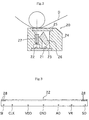
- the image sensor 20 is configured such that a substrate 23 carrying a plurality of LEDs 21 (illumination light sources) and a plurality of image sensor chips 22 (image read elements) is disposed on the bottom of a case 24, a transparent glass cover 25 is placed on the top surface of the case 24, and a light-guide plate 26 for efficiently illuminating the document surface D on the glass cover 25 with the light from the LEDs 21 (light sources) is disposed inside the case 24 together with a rod lens array 27 for converging reflected light from the document surface D on the image sensor chips 22 as a non-inverted image of the same size.
- 1728 light-receiving elements must be arranged in a row at regular intervals to allow an A4 document to be read at a main scanning density of 8 pixels per millimeter.
- Such light-receiving elements can be realized by arranging in a row a plurality of image sensor chips 22 each having a plurality of light-receiving elements 28.
- image sensor chips 22 provided with 96 light-receiving elements are used, 18 image sensor chips 22 are mounted in proximity to each other on the substrate 23 in the longitudinal direction such that all the light-receiving elements have a constant pitch.
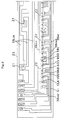
- Fig. 3 schematically shows a planar arrangement of each image sensor chip 22.
- the image sensor chip 22 is obtained by integrating prescribed elements or terminals with a silicon wafer by forming a mask thereon, and dividing the wafer into individual chips by dicing.
- the light-receiving elements 28 are arranged equidistantly at a pitch of 8 elements per millimeter along one edge of the top surface, and serial-in (SI), clock (CLK), logic power supply (VDD), ground (GND), analog-out (AO), serial-out (SO) and other terminal pads are arranged along the other edge of the top surface. These terminal pads are connected by wire bonding to the prescribed wiring patterns on the substrate 23, on which the image sensor chip 22 is mounted.
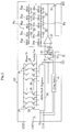
- Fig. 5 depicts an equivalent circuit structure for each image sensor chip 22.
- a plurality of (for example, 96) photoelectric conversion elements (light-receiving elements) such as phototransistors 28 are jointly connected at their emitters to a logic power supply (VDD).
- Analog switches 29 are connected in series to the collectors of the corresponding phototransistors 28. These analog switches 29 are sequentially switched on by a switch circuit 30 actuated by clock signals when this image sensor chip 22 has been selected.
- a shift register is suitable for use as such a switch circuit. Serial-in (SI) signals and clock (CLK) signals are therefore inputted to this shift register 30.
- SI Serial-in
- CLK clock
- a resistance load 31 of prescribed resistance is jointly connected in series between the ground (GND) terminals and the output terminals of the analog switches 29.
- a load capacitor 40 is interposed in parallel to the resistance load 31.
- the resistance load 31 and load capacitor 40 cooperate to constitute an output load for the phototransistors 28.
- the terminal sections of these resistance load 31 and load capacitor 40 on the side of the photoelectric conversion elements are connected to the noninverting input of an operational amplifier 32 (amplification circuit).
- a gain-adjusting resistor R comprising a resistor group Ra and a resistor group Rb is connected to the inverting input of the operational amplifier 32 such that the group Ra is interposed between the inverting input and the ground, and the group Rb is interposed between the inverting input and the output terminal of the operational amplifier 32.
- the gain-adjusting resistor R is configured in the following manner.
- the resistor group Ra is configured such that four adjusting resistors Ra 1 , Ra 2 , Ra 3 and Ra 4 of 2 k ⁇ , 4 k ⁇ , 8 k ⁇ , and 16 k ⁇ , respectively, are connected in series to a 20-k ⁇ reference resistor Ra 0 , and each adjusting resistor is provided with a respective bypass wiring 50 in a parallel arrangement.
- the resistor group Rb is configured such that four adjusting resistors Rb 1 , Rb 2 , Rb 3 and Rb 4 of 20 k ⁇ , 40 k ⁇ , 80 k ⁇ , and 160 k ⁇ , respectively, are connected in series to a 200-k ⁇ reference resistor Rb 0 , and each adjusting resistor is provided with a respective bypass wiring 50 in a parallel arrangement.
- the bypass wirings 50 are fine aluminum wirings formed on a silicon wafer.
- the resistor group Ra is such that only the reference resistor Ra0 is active when all the bypass wirings 50 are connected, and the total resistance of this resistor group Ra is therefore 20 k ⁇ .
- the total resistance of the resistor group Rb is 200 k ⁇ when all the bypass wirings 50 are connected.
- the total resistance of the resistor group Rb should be increased in order to raise the gain G.
- the total resistance of the resistor group Ra should be increased in order to lower the gain G.
- a decision is made as to which of the serially connected adjusting resistors Ra 1 , Ra 2 , Ra 3 , Ra 4 , Rb 1 , Rb 2 , Rb 3 , and Rb 4 constituting these groups should be activated, and the bypass wiring 50 of the selected resistor is cut.
- the resistor group Ra comprises, for example, four adjusting resistors Ra 1 , Ra 2 , Ra 3 , and Ra 4 of 2 k ⁇ , 2 2 k ⁇ , 2 3 k ⁇ , and 2 4 k ⁇ , making it possible to select a resistance ranging from 20 k ⁇ to 50 k ⁇ in 2-k ⁇ increments by selecting any of the adjusting resistors.
- the resistor group Rb makes it possible to select a resistance ranging from 200 k ⁇ to 500 k ⁇ in 20-k ⁇ increments.
- Gain is adjusted using a procedure in which analog output is checked for each chip area under prescribed illumination conditions before the wafer has been divided into individual chips by dicing, the gain needed for the amplifier 32 to yield the analog output level required by the customer or the like is calculated for the analog output available at this stage, and the bypass wiring 50 of the selected adjusting resistor is cut by laser cutting in order to establish the desired total resistance of the resistor group Ra and resistor group Rb.
- laser cutting may, for example, be readily accomplished by scanning an excimer laser beam across the wafer while switching the beam on and off in a controlled manner.
- an analog switch 35 is interposed in parallel with an output load comprising the resistance load 31 and load capacitor 40, and this analog switch 35 is switched on and off by signals from a chip selection circuit 36.
- an analog switch 37 is interposed between the output terminal of the operational amplifier 32 and an analog-out (AO) terminal, and this analog switch 37 is switched on and off by signals from the chip selection circuit 36.
- One end of the shift register 30 is connected to a serial-out (SO) terminal and to the chip selection circuit 36, and serial-in (SI) signals and clock (CLK) signals are inputted to the chip selection circuit 36.
- the chip selection circuit 36 keeps the analog switch 37 on from the moment a pulse signal is inputted to the serial-in (SI) until the moment a pulse signal is outputted from the output of the shift register 30, and keeps the analog switch 35 off during each fall period of the clock pulse.
- SI serial-in
- the image sensor chip 22 thus formed is bonded to the substrate 23 in the following manner. Specifically, as shown in Fig. 4, the logic power (VDD) terminal of each image sensor chip 22 is jointly connected by wire bonding to a logic power wiring pattern 38 VDD on the substrate 23, the ground (GND) terminal to the a ground wiring pattern 38 GND on the substrate, the clock signal (CLK) terminal to a clock signal wiring pattern 38 CLK on the substrate, and the analog-out (AO) terminal to an analog-out wiring pattern 38 AO on the substrate. These terminals are also connected in cascade between the serial-out (SO) terminals and the serial-in (SI) terminals of adjacent image sensor chips via a wiring pattern 38 S on the substrate.
- SO serial-out
- SI serial-in
- the substrate 23 is also provided with wiring patterns 38 LED for installing a plurality of LED chips 21 as illumination light sources, and these wiring patterns are used to arrange the plurality of LED chips 21 at regular intervals.
- the substrate 23 may, for example, be obtained by forming the wiring patterns on a substrate material composed of an alumina ceramic.
- the wiring patterns can, for example, be appropriately formed by screen printing using gold paste. Each wiring pattern is concentrated in a predetermined position on the substrate 23 and is prepared for outside connection by being provided with appropriate connectors or the like.
- the contrast image of a document D on a read line L marked on the glass cover 25 is converged on 1728 light-receiving elements 28. Specifically, light whose intensity corresponds to the contrast image on the read line L strikes the 1728 light-receiving elements arranged in a row.
- the chip selection circuit 36 switches on the analog switch 37 at the analog-out (AO) terminal when a pulse signal has been inputted to this chip from the serial-in (SI) terminal, and this state is maintained until a pulse signal is outputted (SO) from the shift register 30.
- image read data are serially outputted from the analog-out (AO) terminal while the analog switch 37 is on.
- Pulse signals inputted at one end of the shift register 30 are sequentially shifted by clock pulses, and this is accompanied by the sequential energizing of the analog switches 29 connected in series to the phototransistors 28. Phototransistors 28 for outputting read signals are thus sequentially selected. Meanwhile, the chip selection circuit 36 switches on the analog switch 35 during each rise cycle of the clock pulses, and switches off the analog switch 35 during the fall cycles of the clock pulses, with the result that, as indicated by the timing chart in Fig. 6, an electric charge proportional to the intensity of light received by the sequentially selected phototransistors 28 flows through the output load composed of the resistance load 31 and load capacitor 40 during the fall cycles of the clock pulses and the prescribed read cycles of the phototransistors.
- the corresponding microcurrent signals are sensed as the potential of the output loads 31 and 40 on the phototransistor side, this potential is converted to a voltage waveform and amplified in accordance with a prescribed gain by the operational amplifier 32, and the analog data converted to such a voltage waveform are outputted from the analog-out (AO) terminal.
- the pulse signals outputted by the shift register 30 are transmitted from the serial-out (SO) terminal via the pattern on the substrate to the adjacent chip, and the signals sensed by the phototransistors on the adjacent chip are read as serial data in the same manner as above.
- Fig. 6 also depicts the output waveform of the image sensor chip 22 pertaining to the above-described embodiment for a variable intensity of illuminating light. It is evident from the drawing that at the dark level (when there is no illumination with light), clock pulses are not superposed as alternating-current components on the output waveform the way they are superposed in the conventional examples depicted in Figs. 11 and 12. The reason for this is that because the image sensor chip 22 is such that the amplifier circuit 32 and the output loads 31 and 40 are integrated into the image sensor chip 22, a high-impedance output that tends to pick up noise is not brought out to the substrate the way it is brought out in the conventional examples. Consequently, the output waveform exactly matches the intensity of light received by each phototransistor, and, as a result, the image read performance of this image sensor chip is dramatically improved.
- the embodiment described above involves an arrangement in which a resistance load 31 and a load capacitor 40 cooperate as loads for the phototransistors 28 (light-receiving elements).
- the phototransistors 28 output an electric current proportional to the amount of light received during the read cycle in the period during which the analog switch 35 is on. Because of the special properties of the capacitor operating as an output load, the charges that have been retained by the phototransistors 28 immediately flow to this capacitor at this time, making it possible to reduce the amount of charge remaining, in particular, on the bases of the phototransistors 28 when the off-cycle of the analog switch 35 has ended.
- Fig. 7 depicts, in summary form, experimental results obtained when various levels are selected as output loads for the phototransistors 28 to obtain an analog output by separating a document D into “white” section and “black” sections and reading the black sections after reading the white sections.
- the outputs of "white” and “black” readouts are quantitatively shown in Fig. 7, where Fig. 7a pertains to a case in which a resistance of 47 k ⁇ is established as the output load, Fig. 7b pertains to a case in which a resistance of 100 k ⁇ is established as the output load, Fig. 7c pertains to a case in which a capacitor having a capacitance of 33 pF is provided as the output load, Fig.
- Fig. 7d pertains to a case in which a capacitor having a capacitance of 100 pF is provided as the output load
- Fig. 7e pertains to a case in which a capacitor having a capacitance of 200 pF is provided as the output load.
- the corresponding power voltage is 5 V
- the luminous energy of the illumination light source 0.796 ⁇ W
- the read cycle 5 ms and the gain of the operational amplifier 10.
- the bright output waveform outputted from the analog-out (AO) terminal can be varied by including the resistance load 31 into the output load in such a manner and selecting appropriate resistance for this resistance load.
- a comparatively large resistance load results in an output waveform that rises on the right and has a sawtooth shape (as shown in Fig. 8a), but the trailing end of the top portion of the waveform tends to decrease with a reduction in the resistance load.
- the bright output waveform should be as close to a rectangular wave as possible and have a horizontal or roughly horizontal top portion (as shown in Fig. 8b) to achieve optimum processing of image read data. Such a waveform can be obtained by properly selecting the resistance of the resistance load.
- the subject invention is such that the output from the image sensor chip represents a voltage waveform that is free from noise and is already amplified to the desired gain level, dispensing with the need to adopt noise-suppressing actions for the substrate or to mount amplifier circuits, adjusting varistors, or other electronic components on the substrate. It is thus possible to use products obtained by forming wiring patterns on one side. Such substrates can be fabricated by performing the simple step of forming wiring patterns on alumina ceramic substrates by means of screen printing. Such fabrication can be further facilitated because the wiring patterns may be formed on only one side. In addition, the output level of each image sensor chip can be adjusted individually, making it possible to prevent read characteristics from being adversely affected by variations in the read level of each chip at different locations in the main scanning direction.
- the proposed image sensor chip 22 or image sensor 20 which is obtained by adopting a substrate 23 on which the image sensor chips and LED chips (light sources) are mounted on one side in the manner described above, is devoid of the irregularities created by mounting outside components on the back side, has an excellent appearance, is very easy to handle, and is made smaller in the thickness direction.
- the analog switches connected in series to the photoelectric conversion elements may also be connected to the terminals of the photoelectric conversion elements on the power supply side.
- the load capacitor 40 and the resistance load 31, other than being jointly connected to the photoelectric conversion elements on the ground side (as in the embodiment), may also be jointly connected on the power supply side, and the potential difference between their terminals may be amplified by an amplifier circuit.
- a resistance load 31 and a load capacitor 40 connected in parallel were used as the output load components of the phototransistors in the embodiment described above, it is also possible to use a load consisting solely of the resistance load 31 (as shown in Fig. 9) or load capacitor 40 (as shown in Fig. 10).
- the image sensor chip of the claimed invention is suitable for use as an element constituting the image sensor of a fax machine, image scanner, or other image reader.
Landscapes
- Engineering & Computer Science (AREA)
- Multimedia (AREA)
- Signal Processing (AREA)
- Physics & Mathematics (AREA)
- Electromagnetism (AREA)
- Facsimile Heads (AREA)
Abstract
Description
Claims (10)
- An image sensor chip manufactured by integrating:a prescribed number of photoelectric conversion elements as photoreceptors;analog switches connected in series to the corresponding photoelectric conversion elements; anda switch circuit for sequentially switching on said analog switches in accordance with clock signals; wherein said image sensor chip is characterized by further comprising:output load components jointly connected in series to sets composed of said photoelectric conversion elements and their respective analog switches; andan amplification circuit for amplifying the potential of said output load components on the side of the photoelectric conversion elements.
- An image sensor chip, characterized by comprising:a power terminal;a ground terminal;a clock signal input terminal;an analog signal output terminal;photoelectric conversion elements arranged in a row at regular intervals and connected at one end to the power terminal;analog switches connected to the respective output terminals of the photoelectric conversion elements;a switch circuit for sequentially switching on said analog switches in accordance with clock signals;output load components jointly interposed between the ground terminal and the output terminals of said analog switches; andan amplification circuit for amplifying the potential of said output load components on the side of the photoelectric conversion elements; wherein the structure is such that the output of said amplification circuit is outputted to the analog signal output terminal.
- The image sensor chip according to Claim 1 or 2, wherein said output load is a load resistor.
- The image sensor chip according to Claim 1 or 2, wherein said output load is a load capacitor.
- The image sensor chip according to Claim 1 or 2, wherein said output load consists of a load resistor and a load capacitor connected in parallel to each other.
- The image sensor chip according to any of Claims 1 through 5, wherein the gain-adjusting resistor of said amplification circuit is also fabricated in integral form, and said gain-adjusting resistor comprises a plurality of resistors connected in series and cuttable bypass wirings provided to all or some of said plurality of resistors.
- The image sensor chip according to Claim 6, whereinsaid amplification circuit is an operational amplifier;said gain-adjusting resistor comprises a resistor group interposed between the inverting input of said operational amplifier and the output of this operational amplifier, and a resistor group interposed between the ground and the inverting input of said operational amplifier; andeach resistor group comprises a plurality of resistors connected in series and cuttable bypass wirings provided to all or some of these resistors.
- A method for manufacturing an image sensor chip, characterized in that an image sensor chip according to Claim 6 or 7 is used as a constituent unit, and a wafer obtained by integrating a plurality of such units is fabricated;the gain of said amplification circuit is adjusted by cutting with a laser the bypass wirings of resistors selected from the plurality of resistors constituting said gain-adjusting resistor of each chip unit at the wafer stage; andsaid wafer is divided into image sensor chips by dicing.
- An image sensor substrate, characterized in that a plurality of image sensor chips according to any of Claims 1 through 7 are mounted on one side together with one or more light-emitting elements as light sources.
- An image sensor, characterized in that an image sensor substrate according to Claim 9 is attached to the bottom surface of a case, a glass cover is placed on the top surface of the case, and reflected light from a document on the glass cover illuminated by said light-emitting elements is converged on the photoelectric conversion elements of said image sensor chips.
Applications Claiming Priority (7)
| Application Number | Priority Date | Filing Date | Title |
|---|---|---|---|
| JP9226896 | 1996-04-15 | ||
| JP9226896 | 1996-04-15 | ||
| JP9226996 | 1996-04-15 | ||
| JP9226796 | 1996-04-15 | ||
| JP9226796 | 1996-04-15 | ||
| JP9226996 | 1996-04-15 | ||
| PCT/JP1997/001305 WO1997039486A1 (en) | 1996-04-15 | 1997-04-15 | Image sensor chip, method for manufacturing the same, and image sensor |
Publications (3)
| Publication Number | Publication Date |
|---|---|
| EP0924770A1 true EP0924770A1 (en) | 1999-06-23 |
| EP0924770A4 EP0924770A4 (en) | 1999-07-21 |
| EP0924770B1 EP0924770B1 (en) | 2006-08-09 |
Family
ID=27306984
Family Applications (1)
| Application Number | Title | Priority Date | Filing Date |
|---|---|---|---|
| EP97915730A Expired - Lifetime EP0924770B1 (en) | 1996-04-15 | 1997-04-15 | Image sensor chip, method for manufacturing the same, and image sensor |
Country Status (7)
| Country | Link |
|---|---|
| US (2) | US6169279B1 (en) |
| EP (1) | EP0924770B1 (en) |
| KR (1) | KR100384360B1 (en) |
| CN (1) | CN1163969C (en) |
| DE (1) | DE69736479T2 (en) |
| TW (1) | TW350621U (en) |
| WO (1) | WO1997039486A1 (en) |
Families Citing this family (9)
| Publication number | Priority date | Publication date | Assignee | Title |
|---|---|---|---|---|
| JP2003087514A (en) * | 2000-11-15 | 2003-03-20 | Nippon Sheet Glass Co Ltd | Image reader apparatus, its light source, and shading correction apparatus |
| JP2003115584A (en) * | 2001-10-05 | 2003-04-18 | Canon Inc | Imaging device and reading device |
| US20050110464A1 (en) * | 2003-11-25 | 2005-05-26 | Baker Howard S. | Fuel cell voltage monitoring system |
| JP2006072058A (en) * | 2004-09-03 | 2006-03-16 | Pentax Corp | Laser scanning device |
| US7528040B2 (en) | 2005-05-24 | 2009-05-05 | Cree, Inc. | Methods of fabricating silicon carbide devices having smooth channels |
| JP5170501B2 (en) * | 2006-05-16 | 2013-03-27 | 株式会社デンソー | Power converter |
| JP2017220893A (en) * | 2016-06-10 | 2017-12-14 | 株式会社村田製作所 | amplifier |
| US10944882B2 (en) * | 2017-12-01 | 2021-03-09 | Hewlett-Packard Development Company, L.P. | Image sensor line orientation |
| CN117008369B (en) * | 2023-09-27 | 2023-12-22 | 惠科股份有限公司 | Display panel, resistance verification method of display panel and display device |
Family Cites Families (12)
| Publication number | Priority date | Publication date | Assignee | Title |
|---|---|---|---|---|
| DE3435354A1 (en) * | 1983-09-27 | 1986-01-23 | Kyocera Corp., Kyoto | PHOTOELECTRIC CONVERTER ARRANGEMENT |
| JPS63108808A (en) * | 1986-10-24 | 1988-05-13 | Mitsubishi Electric Corp | Preamplifier incorporating photodetector |
| US4886977A (en) * | 1986-11-11 | 1989-12-12 | Canon Kabushiki Kaisha | Photoelectric converter provided with voltage dividing means |
| JP2669462B2 (en) | 1987-08-05 | 1997-10-27 | キヤノン株式会社 | Photoelectric conversion device |
| JPH01208974A (en) | 1988-02-16 | 1989-08-22 | Sony Corp | Mos type solid-state image pickup device |
| JPH0220065A (en) | 1988-07-08 | 1990-01-23 | Ricoh Co Ltd | Line sensor |
| JPH0247979A (en) * | 1988-08-09 | 1990-02-16 | Fuji Xerox Co Ltd | Picture reader |
| JP2823578B2 (en) * | 1989-02-10 | 1998-11-11 | キヤノン株式会社 | Photoelectric conversion device and driving method thereof |
| JPH06273602A (en) | 1993-03-24 | 1994-09-30 | Matsushita Electric Ind Co Ltd | Contact image sensor |
| JP2991039B2 (en) * | 1994-06-16 | 1999-12-20 | 三菱電機株式会社 | Contact image sensor |
| JPH0888807A (en) | 1994-09-16 | 1996-04-02 | Canon Inc | Image sensor |
| US6128039A (en) * | 1999-01-11 | 2000-10-03 | Omnivision Technologies, Inc. | Column amplifier for high fixed pattern noise reduction |
-
1997
- 1997-04-15 KR KR10-1998-0708203A patent/KR100384360B1/en not_active Expired - Fee Related
- 1997-04-15 WO PCT/JP1997/001305 patent/WO1997039486A1/en not_active Ceased
- 1997-04-15 CN CNB971936757A patent/CN1163969C/en not_active Expired - Lifetime
- 1997-04-15 DE DE69736479T patent/DE69736479T2/en not_active Expired - Fee Related
- 1997-04-15 US US09/171,243 patent/US6169279B1/en not_active Expired - Lifetime
- 1997-04-15 TW TW086219705U patent/TW350621U/en unknown
- 1997-04-15 EP EP97915730A patent/EP0924770B1/en not_active Expired - Lifetime
-
2000
- 2000-10-17 US US09/690,546 patent/US6468827B1/en not_active Expired - Lifetime
Also Published As
| Publication number | Publication date |
|---|---|
| DE69736479T2 (en) | 2007-04-12 |
| US6169279B1 (en) | 2001-01-02 |
| KR20000005441A (en) | 2000-01-25 |
| EP0924770B1 (en) | 2006-08-09 |
| CN1215502A (en) | 1999-04-28 |
| KR100384360B1 (en) | 2003-11-17 |
| WO1997039486A1 (en) | 1997-10-23 |
| TW350621U (en) | 1999-01-11 |
| DE69736479D1 (en) | 2006-09-21 |
| US6468827B1 (en) | 2002-10-22 |
| EP0924770A4 (en) | 1999-07-21 |
| CN1163969C (en) | 2004-08-25 |
Similar Documents
| Publication | Publication Date | Title |
|---|---|---|
| US6195183B1 (en) | Image reading apparatus and image sensor chip thererfor | |
| US6169279B1 (en) | Image sensor chip, method for manufacturing the same, and image sensor therefor | |
| US4473842A (en) | Apparatus and method for examining printed circuit board provided with electronic parts | |
| JPH089099A (en) | Contact image sensor | |
| US6376822B1 (en) | Image reading apparatus | |
| US7167284B2 (en) | Image sensor head provided with separate CCD sensor chip and driver chip | |
| KR100886034B1 (en) | Image sensor | |
| US6184513B1 (en) | Image sensor chip and image sensor | |
| JP4725901B2 (en) | Optical detector | |
| JPH09284470A (en) | Picture reading/writing head | |
| JPWO1997039486A1 (en) | Image sensor chip, method of manufacturing the same, and image sensor | |
| US7164509B2 (en) | Image reader having image sensor ICS divided into plural blocks having simultaneously read-out image signals | |
| JP3771368B2 (en) | Image sensor chip arrangement method and image reading apparatus using the arrangement method | |
| JP4540138B2 (en) | Image sensor array | |
| US7170651B2 (en) | Image reader | |
| JPS6217877B2 (en) | ||
| JPH0686006A (en) | Image sensor | |
| JPH05308466A (en) | Image sensor | |
| JP3140437B2 (en) | Image sensor | |
| JPS623630B2 (en) | ||
| JPH01246865A (en) | Hybrid integrated photoelectric conversion element array | |
| JP2007173926A (en) | Image sensor | |
| JPS59134979A (en) | Light sensor array device | |
| JPS5981967A (en) | image input device | |
| JPS6155959A (en) | Original reader |
Legal Events
| Date | Code | Title | Description |
|---|---|---|---|
| PUAI | Public reference made under article 153(3) epc to a published international application that has entered the european phase |
Free format text: ORIGINAL CODE: 0009012 |
|
| 17P | Request for examination filed |
Effective date: 19981027 |
|
| AK | Designated contracting states |
Kind code of ref document: A1 Designated state(s): DE FR GB NL |
|
| A4 | Supplementary search report drawn up and despatched |
Effective date: 19990609 |
|
| AK | Designated contracting states |
Kind code of ref document: A4 Designated state(s): DE FR GB NL |
|
| GRAP | Despatch of communication of intention to grant a patent |
Free format text: ORIGINAL CODE: EPIDOSNIGR1 |
|
| GRAS | Grant fee paid |
Free format text: ORIGINAL CODE: EPIDOSNIGR3 |
|
| GRAA | (expected) grant |
Free format text: ORIGINAL CODE: 0009210 |
|
| AK | Designated contracting states |
Kind code of ref document: B1 Designated state(s): DE FR GB NL |
|
| REG | Reference to a national code |
Ref country code: GB Ref legal event code: FG4D |
|
| REF | Corresponds to: |
Ref document number: 69736479 Country of ref document: DE Date of ref document: 20060921 Kind code of ref document: P |
|
| ET | Fr: translation filed | ||
| PLBE | No opposition filed within time limit |
Free format text: ORIGINAL CODE: 0009261 |
|
| STAA | Information on the status of an ep patent application or granted ep patent |
Free format text: STATUS: NO OPPOSITION FILED WITHIN TIME LIMIT |
|
| 26N | No opposition filed |
Effective date: 20070510 |
|
| PGFP | Annual fee paid to national office [announced via postgrant information from national office to epo] |
Ref country code: NL Payment date: 20080415 Year of fee payment: 12 |
|
| PGFP | Annual fee paid to national office [announced via postgrant information from national office to epo] |
Ref country code: FR Payment date: 20090417 Year of fee payment: 13 Ref country code: DE Payment date: 20090409 Year of fee payment: 13 |
|
| PGFP | Annual fee paid to national office [announced via postgrant information from national office to epo] |
Ref country code: GB Payment date: 20090415 Year of fee payment: 13 |
|
| NLV4 | Nl: lapsed or anulled due to non-payment of the annual fee |
Effective date: 20091101 |
|
| PG25 | Lapsed in a contracting state [announced via postgrant information from national office to epo] |
Ref country code: NL Free format text: LAPSE BECAUSE OF NON-PAYMENT OF DUE FEES Effective date: 20091101 |
|
| GBPC | Gb: european patent ceased through non-payment of renewal fee |
Effective date: 20100415 |
|
| REG | Reference to a national code |
Ref country code: FR Ref legal event code: ST Effective date: 20101230 |
|
| PG25 | Lapsed in a contracting state [announced via postgrant information from national office to epo] |
Ref country code: DE Free format text: LAPSE BECAUSE OF NON-PAYMENT OF DUE FEES Effective date: 20101103 |
|
| PG25 | Lapsed in a contracting state [announced via postgrant information from national office to epo] |
Ref country code: GB Free format text: LAPSE BECAUSE OF NON-PAYMENT OF DUE FEES Effective date: 20100415 |
|
| PG25 | Lapsed in a contracting state [announced via postgrant information from national office to epo] |
Ref country code: FR Free format text: LAPSE BECAUSE OF NON-PAYMENT OF DUE FEES Effective date: 20100430 |