EP0924589A1 - Electroactuator control device and method for controlling this control device - Google Patents
Electroactuator control device and method for controlling this control device Download PDFInfo
- Publication number
- EP0924589A1 EP0924589A1 EP98830380A EP98830380A EP0924589A1 EP 0924589 A1 EP0924589 A1 EP 0924589A1 EP 98830380 A EP98830380 A EP 98830380A EP 98830380 A EP98830380 A EP 98830380A EP 0924589 A1 EP0924589 A1 EP 0924589A1
- Authority
- EP
- European Patent Office
- Prior art keywords
- control
- voltage
- terminal
- piloting
- block
- Prior art date
- Legal status (The legal status is an assumption and is not a legal conclusion. Google has not performed a legal analysis and makes no representation as to the accuracy of the status listed.)
- Granted
Links
Images





Classifications
-
- F—MECHANICAL ENGINEERING; LIGHTING; HEATING; WEAPONS; BLASTING
- F02—COMBUSTION ENGINES; HOT-GAS OR COMBUSTION-PRODUCT ENGINE PLANTS
- F02D—CONTROLLING COMBUSTION ENGINES
- F02D41/00—Electrical control of supply of combustible mixture or its constituents
- F02D41/20—Output circuits, e.g. for controlling currents in command coils
-
- G—PHYSICS
- G05—CONTROLLING; REGULATING
- G05F—SYSTEMS FOR REGULATING ELECTRIC OR MAGNETIC VARIABLES
- G05F1/00—Automatic systems in which deviations of an electric quantity from one or more predetermined values are detected at the output of the system and fed back to a device within the system to restore the detected quantity to its predetermined value or values, i.e. retroactive systems
- G05F1/10—Regulating voltage or current
- G05F1/46—Regulating voltage or current wherein the variable actually regulated by the final control device is DC
- G05F1/56—Regulating voltage or current wherein the variable actually regulated by the final control device is DC using semiconductor devices in series with the load as final control devices
-
- F—MECHANICAL ENGINEERING; LIGHTING; HEATING; WEAPONS; BLASTING
- F02—COMBUSTION ENGINES; HOT-GAS OR COMBUSTION-PRODUCT ENGINE PLANTS
- F02D—CONTROLLING COMBUSTION ENGINES
- F02D41/00—Electrical control of supply of combustible mixture or its constituents
- F02D41/20—Output circuits, e.g. for controlling currents in command coils
- F02D2041/2003—Output circuits, e.g. for controlling currents in command coils using means for creating a boost voltage, i.e. generation or use of a voltage higher than the battery voltage, e.g. to speed up injector opening
-
- F—MECHANICAL ENGINEERING; LIGHTING; HEATING; WEAPONS; BLASTING
- F02—COMBUSTION ENGINES; HOT-GAS OR COMBUSTION-PRODUCT ENGINE PLANTS
- F02D—CONTROLLING COMBUSTION ENGINES
- F02D41/00—Electrical control of supply of combustible mixture or its constituents
- F02D41/20—Output circuits, e.g. for controlling currents in command coils
- F02D2041/2003—Output circuits, e.g. for controlling currents in command coils using means for creating a boost voltage, i.e. generation or use of a voltage higher than the battery voltage, e.g. to speed up injector opening
- F02D2041/2006—Output circuits, e.g. for controlling currents in command coils using means for creating a boost voltage, i.e. generation or use of a voltage higher than the battery voltage, e.g. to speed up injector opening by using a boost capacitor
-
- F—MECHANICAL ENGINEERING; LIGHTING; HEATING; WEAPONS; BLASTING
- F02—COMBUSTION ENGINES; HOT-GAS OR COMBUSTION-PRODUCT ENGINE PLANTS
- F02D—CONTROLLING COMBUSTION ENGINES
- F02D41/00—Electrical control of supply of combustible mixture or its constituents
- F02D41/20—Output circuits, e.g. for controlling currents in command coils
- F02D2041/2003—Output circuits, e.g. for controlling currents in command coils using means for creating a boost voltage, i.e. generation or use of a voltage higher than the battery voltage, e.g. to speed up injector opening
- F02D2041/201—Output circuits, e.g. for controlling currents in command coils using means for creating a boost voltage, i.e. generation or use of a voltage higher than the battery voltage, e.g. to speed up injector opening by using a boost inductance
-
- F—MECHANICAL ENGINEERING; LIGHTING; HEATING; WEAPONS; BLASTING
- F02—COMBUSTION ENGINES; HOT-GAS OR COMBUSTION-PRODUCT ENGINE PLANTS
- F02D—CONTROLLING COMBUSTION ENGINES
- F02D41/00—Electrical control of supply of combustible mixture or its constituents
- F02D41/20—Output circuits, e.g. for controlling currents in command coils
- F02D2041/202—Output circuits, e.g. for controlling currents in command coils characterised by the control of the circuit
- F02D2041/2024—Output circuits, e.g. for controlling currents in command coils characterised by the control of the circuit the control switching a load after time-on and time-off pulses
- F02D2041/2027—Control of the current by pulse width modulation or duty cycle control
-
- F—MECHANICAL ENGINEERING; LIGHTING; HEATING; WEAPONS; BLASTING
- F02—COMBUSTION ENGINES; HOT-GAS OR COMBUSTION-PRODUCT ENGINE PLANTS
- F02D—CONTROLLING COMBUSTION ENGINES
- F02D41/00—Electrical control of supply of combustible mixture or its constituents
- F02D41/20—Output circuits, e.g. for controlling currents in command coils
- F02D2041/202—Output circuits, e.g. for controlling currents in command coils characterised by the control of the circuit
- F02D2041/2031—Control of the current by means of delays or monostable multivibrators
-
- F—MECHANICAL ENGINEERING; LIGHTING; HEATING; WEAPONS; BLASTING
- F02—COMBUSTION ENGINES; HOT-GAS OR COMBUSTION-PRODUCT ENGINE PLANTS
- F02D—CONTROLLING COMBUSTION ENGINES
- F02D41/00—Electrical control of supply of combustible mixture or its constituents
- F02D41/20—Output circuits, e.g. for controlling currents in command coils
- F02D2041/2086—Output circuits, e.g. for controlling currents in command coils with means for detecting circuit failures
- F02D2041/2093—Output circuits, e.g. for controlling currents in command coils with means for detecting circuit failures detecting short circuits
Definitions
- the present invention relates to an electroactuator control device and to a method for controlling this control device.
- control device can be used advantageously, but need not be used exclusively, to control electroinjectors of an injection system for an internal combustion engine of the petrol, diesel, methane or LPG-operated type, to which the following description will make specific reference, without however detracting from general applicability.
- control device can also be applied to any other type of electroactuator, such as solenoid valves of ABS devices and the like, and solenoid valves of variable phasing systems etc.
- control devices are used in which the electroinjectors are connected on the one hand to a low voltage supply source, and on the other hand to an earthing line, by means of a controlled electronic switch.
- control devices for electroinjectors which are connected on the one hand to earth, and on the other hand to an internal node of the control devices themselves, such that any short-circuit to earth of one of the terminals of the electroinjectors does not give rise to damage to the control device, and thus to stalling of the vehicle, but simply puts that individual electroinjector out of use, so that the vehicle can continue to run with one electroinjector short.
- the object of the present invention is to produce an electroactuator control device which is simple, economical, and makes it possible to eliminate the above-described disadvantages.
- an electroactuator control device is provided, as described in claim 1.
- the present invention also relates to a method for controlling this control device, as described in claim 23.
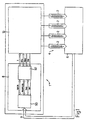
- the control device 1 comprises a timing circuit 8 which receives as input data signals S which are measured on the engine 6, in particular speed and angular position of the engine 6 and injection advance, and which generates as output timing signals T and state signals H/L which are used to control the electroinjectors 2; it also comprises a piloting circuit 10 which receives as input the timing signals T and the state signals H/L, and has the function of piloting the electroinjectors 2 on the basis of the timing signals T and of the state signals H/L, as well as of generating reaction signals FBI, FBV1 and FBV2 for the timing circuit 8, in the manner described in greater detail hereinafter.
- a timing circuit 8 which receives as input data signals S which are measured on the engine 6, in particular speed and angular position of the engine 6 and injection advance, and which generates as output timing signals T and state signals H/L which are used to control the electroinjectors 2; it also comprises a piloting circuit 10 which receives as input the timing signals T and the state signals H/L, and has the
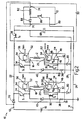
- the piloting circuit 10 comprises a first and a second input terminal 12, 14, which can be connected respectively to a positive pole and a negative pole of an electrical energy source 16, for example a battery of the vehicle, and a plurality of pairs of output terminals, one for each electroinjector 2, each of which comprises a first and a second output terminal 18, 20, between which a respective electroinjector 2 is connected in use.
- the piloting circuit 10 additionally comprises a supply line 22, which is connected in the manner described in greater detail hereinafter to the first input terminal 12; an earthing line 24 which is directly connected to the second input terminal 14 and to the electrical earth of the vehicle; and an internal connection line 26.
- the piloting circuit 10 additionally comprises a plurality of circuits 30 for controlling the electroinjectors 2, one for each electroinjector 2, connected to the supply and earthing lines 22, 24 and to the timing circuit 8, and each interposed between the first and the second input terminal 12, 14 and a respective pair of output terminals 18, 20, which receive as input the timing signals T and the state signals H/L, and are activated selectively by the timing signals T themselves in order to control the respective electroactuators 2.
- Each control circuit 30 comprises a first piloting transistor 34 of the MOSFET type, which has a control terminal connected to the timing circuit 8, and receives from the latter a first timing signal T 1 , a sink terminal which is connected to the supply line 22, and a source terminal which is connected to the first output terminal 18; and a second piloting transistor 36 of the MOSFET type, which has a control terminal connected to the timing circuit 8, and receives from the latter a second timing signal T 2 , a sink terminal which is connected to the second output terminal 20, and a source terminal which is connected to the earthing line 24 by means of a shunt resistor 38.
- Each control circuit 30 also comprises a discharge diode 40, the anode of which is connected to the earthing line 24, and the cathode of which is connected to the first output terminal 18.
- Each control circuit 30 also comprises a comparator circuit 42, which has a first input terminal 44 connected to the source terminal of the second piloting transistor 36, i.e. which is connected to a terminal of the shunt resistor 38, a second input terminal 46 which is connected to the timing circuit 8 and receives from the latter a state signal H/L, and an output terminal 48 to which it supplies a first reaction signal FBI which is supplied to the timing circuit 8 itself.
- a comparator circuit 42 which has a first input terminal 44 connected to the source terminal of the second piloting transistor 36, i.e. which is connected to a terminal of the shunt resistor 38, a second input terminal 46 which is connected to the timing circuit 8 and receives from the latter a state signal H/L, and an output terminal 48 to which it supplies a first reaction signal FBI which is supplied to the timing circuit 8 itself.
- the state signal H/L is a digital-type voltage signal, and assumes a high logic level which is defined by a first voltage value, for example 5 volts, and a low logic level which is defined by a second voltage value which is lower than the first, for example 0 volt.
- the state signal H/L switches from the high logic level to the low logic level during control of the corresponding electroinjector 2, in the manner described in greater detail hereinafter.
- the comparator circuit 42 has the purpose of comparing the voltage of the source terminal of the piloting transistor 36, relative to the voltage of the earthing line 24, with the voltage value assumed by the state signal H/L, in order to generate the first reaction signal FBI according to the result of the comparison.
- the first reaction signal FBI is a digital-type voltage signal which indicates whether or not current is passing in the corresponding electroinjector 2, and assumes a first logic level, for example the high logic level, when the voltage at the ends of the shunt resistor 38 is greater than the voltage value assumed by the first state signal H/L (i.e. when current is passing in the corresponding electroinjector 2), and it assumes a second logic level, the low logic level in the example in question, when the voltage at the ends of the shunt resistor 38 is the same as, or lower than the voltage value assumed by the first state signal H/L (i.e. when current is not passing in the corresponding electroinjector 2).
- a first logic level for example the high logic level
- the first reaction signal FBI is used by the timing circuit 8 in order to carry out a closed-loop check on the current which is flowing in the corresponding electroinjector 2, in the manner described in detail hereinafter.
- Each control circuit 30 additionally comprises a first voltage-limiting circuit 52 which has an input terminal 54 which is connected to the source terminal of the first piloting transistor 34, i.e. which is connected to the first output terminal 18 of the control circuit 30 itself, and an output terminal 56 to which it supplies a second reaction signal FBV1, which is supplied to the timing circuit 8.
- the first voltage-limiting circuit 52 has the purpose of supplying to the output terminal 56 a second reaction signal FBV1, which is obtained by limiting the dynamics of the voltage of the source terminal of the first piloting transistor 34, which is typically variable between 0 and 12 volts.
- the second reaction signal FBV1 is a voltage signal substantially of the digital type, which is indicative of the voltage value assumed by the so-called "hot side" of the corresponding electroinjector 2, and assumes a high logic level which is defined by the first voltage value, for example 5 volts, when the hot side of the corresponding electroinjector 2 is set to a voltage which is close to the voltage of the positive pole of the electrical energy source 16, and it assumes a low logic value which is defined by a second voltage value lower than the first, for example 0 volt, when the hot side of the corresponding electroinjector 2 is set to a voltage which is close to the voltage of the negative pole of the electrical energy source 16 (earthing voltage).
- Each control circuit 30 additionally comprises a second voltage-limiting circuit 62 which has an input terminal 64 connected to the sink terminal of the second piloting transistor 36, i.e. which is connected to the second output terminal 18 of the control circuit 30 itself, and an output terminal 66 to which it supplies a third reaction signal FBV2 which is supplied to the timing circuit 8.
- the second voltage-limiting circuit 62 has the purpose of supplying to the output terminal 66 a third reaction signal FBV2 which is obtained by limiting the dynamics of the voltage of the sink terminal of the second piloting transistor 36, which is typically variable between 0 and 12 volts.
- the third reaction signal FBV2 is a voltage signal substantially of the digital type, which is indicative of the voltage value present at the so-called "cold side" of the corresponding electroinjector 2, and assumes a high logic level which is defined by a first voltage value, for example 5 volts, when the cold side of the electroinjector 2 is set to a voltage which is close to the voltage of the positive pole of the electrical energy source 16, and it assumes a low logic value which is defined by a second voltage value lower than the first, for example 0 volt, when the cold side of the electroinjector 2 is set to a voltage which is close to the voltage of the negative pole of the electrical energy source 16 (earthing voltage).
- a first voltage value for example 5 volts
- the second and third reaction signals FBV1 and FBV2 are used by the timing circuit 8 in order to carry out monitoring of the malfunctioning of the corresponding electroinjector 2, in the manner described in detail hereinafter.
- the voltage-increasing circuit 32 comprises a load diode 70 (shown outside the voltage-increasing circuit 32 purely for reasons of convenience of representation), which is interposed between the first input terminal 12 of the piloting circuit 10 and the supply line 22, and which in particular has the anode connected to the first input terminal 12 and the cathode connected to the supply line 22; a voltage converter 72 of the DC/DC type (switching converter of the direct current/direct current type, to increase the input voltage), for generation of a voltage which is greater than that supplied by the electrical energy source 16, with an input terminal 74 connected to the first input terminal 12, a first output terminal 76 connected to the supply line 22 via a transfer transistor 78, and a second output terminal 80 connected to the earthing line 24.
- a load diode 70 shown outside the voltage-increasing circuit 32 purely for reasons of convenience of representation
- the load diode 70 defines a controlled switch which permits selective connection between the supply line 22 and the first input terminal 12 of the piloting circuit 10, on the basis of the voltage value present at the ends of the load diode 70 itself.
- the transfer transistor 78 is a MOSFET transistor which has a control terminal connected to the timing circuit 8, and receives from the latter a third timing signal T 3 , a sink terminal connected to the first output terminal 76 of the voltage converter 72, and a source terminal connected to the supply line 22.
- the voltage converter 72 which is of a known type and is therefore not described in detail, substantially comprises an inductor 82 which has a first terminal connected to the first input terminal 74, and a second terminal connected to the anode of a transfer diode 84, the cathode of which is connected to the first output terminal 76.
- the voltage converter 72 additionally comprises a load transistor 86 of the MOSFET type with a control terminal which receives (from a controller which is of a known type and is not illustrated) a control signal for piloting of the load transistor 86 itself in the event of saturation or cut-off, a sink terminal which is connected to the anode of the transfer diode 84, and a source terminal which is connected to the earthing line 24.
- the high voltage circuit 32 additionally comprises a capacitor 88 which has a first and a second terminal connected respectively to the first output terminal 76 of the voltage converter 72 and to the earthing line 24.
- the voltage-increasing circuit 32 additionally comprises a plurality of recirculation diodes 89, one for each control circuit 30 (shown outside the voltage-increasing circuit 32 purely for reasons of convenience of representation), which has the anodes connected to respective second output terminals 20 of the piloting circuit 10, and the cathodes connected to the first output terminal 76 of the voltage converter 72.
- the timing circuit 8 comprises a microprocessor 90 which receives as input the data signals S measured on the engine 6, and which, on the basis of the data signals S, generates as output operative data for control of the injectors 2; and a control circuit 92 which is connected at its input to the microprocessor 90, and which, in addition to the operative data supplied by the microprocessor 90 itself, receives the first, the second and third reaction signals FBI, FBV1 and FBV2 generated by the piloting circuit 10, and generates as output, on the basis of the said operating data and the reaction signals FBI, FBV1 and FBV2, the timing signals T for the piloting circuit 10 itself, thus implementing the control method which is the subject of the present invention.
- the control circuit 92 also generates as output an interrupt signal INT which is supplied to the microprocessor 90 in order to interrupt its operations in particular operating situations, as described in greater detail hereinafter.
- the microprocessor 90 on the basis of data signals S, the microprocessor 90 generates as output a first and second series of binary data i.e. DATA, ADDRESS, which indicates the temporal duration of the intervals of activation of the piloting transistors 34 and 36, and of the transfer transistor 78 of the piloting circuit 10, which data is supplied to the control circuit 92 via data BUS lines.
- DATA binary data
- ADDRESS binary data
- the timing circuit 8 activates each control circuit 30 selectively by supplying the timing signals T 1 , T 2 , T 3 to the control terminals of the corresponding piloting transistors 34 and 36, as well as to the control terminal of the transfer transistor 78 of the voltage-increasing circuit 32.
- the timing signals T 1 , T 2 , T 3 are digital-type voltage signals and assume a high logic level, i.e. a logic level 1, for example of 5 volts, and a low logic level, i.e. a logic level 0, for example of 0 volt, in order to control the piloting transistors 34, 36 and the transfer transistor 78 respectively in the event of saturation and cut-off; each transistor therefore acts as an open or closed switch.
- control device 1 will now be described with reference to piloting of a single one of the electroinjectors 2, and thus the functioning will be described of a single one of the control circuits 30, which cooperates with the voltage-increasing circuit 32 for supply of the corresponding electroinjector 2.
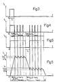
- control circuit 30 will refer to figures 3-6, which illustrate the development over a period of time of the timing signals T 1 , T 2 , T 3 of the piloting transistors 34, 36 and the transfer transistor 78, as well as of the current I L which flows in the electroinjector 2.
- the voltage converter 72 loads the capacitor 88 in a known manner such that at its ends there is present a voltage V C which is greater than the voltage V B supplied by the electrical energy source 16.
- the capacitor 88 and the inductor 82 are connected to one another in series via the transfer diode 84, and thus current flows in the loop defined by the inductor 82, the transfer diode 84 and the capacitor 88, which loads the capacitor 88 and gives rise to an increase in the voltage at its ends.
- the timing circuit 8 commands opening of the piloting transistors 34, 36 and the transfer transistor 78, and thus the control circuit 30 is inactive, and there is no electrical connection between the voltage-increasing circuit 32 and the supply line 22.
- the timing circuit 8 initially commands closing of the piloting transistors 34, 36 and the discharge transistor 78, for a pre-determined interval of time, indicated as t 1 in figures 3 and 6, and starting from an instant of time indicated as t 0 , thus starting the so-called "LAUNCHING STEP", in which there is generated a current which increases rapidly over a period of time, up to a value which is sufficient to command opening of the electroinjector 2.
- the transfer transistor 78 connects the supply line 22 to the first terminal of the capacitor 88, thus determining the existence of a difference in voltage between the supply line 22 itself and the earthing line 24, which difference is equivalent to the voltage V C which exists at the ends of the capacitor 88.
- the capacitor 88 is kept loaded with the voltage V C by the voltage converter 72, in the manner previously described.
- the current I L which flows in the electroinjector 2 increases substantially linearly, with a slope which is equivalent to V C /L, in which L is the equivalent inductance of the electroinjector 2 and V C is the voltage at the ends of the capacitor, up to a value I 1 which is equivalent to V C *t 1 /L, such as to command instantaneous opening of the electroinjector 2 itself.
- the timing circuit 8 commands opening of the transfer transistor 78, thus determining interruption of the connection between the supply line 22 and the capacitor 88, and the start of the so-called "BYPASS STEP", in which the current which flows in the electroinjector 2 is maintained around an average value, such as to command opening of the electroinjector 2.
- the timing circuit 8 commands closing and opening of the piloting transistor 34 repeatedly, and for a pre-determined time interval which is indicated as t BYPASS in figures 4 and 6, such that the current which flows in the electroinjector 2 assumes a sawtooth development which has a duration t p , and oscillates around a first average pre-determined value, for example 20 A, which is indicated as I TH1 in figure 6.
- connection transistor 78 when the connection transistor 78 is opened, since the piloting transistor 34 is closed, the timing circuit 8 continues to keep the latter closed for a pre-determined time interval, which is indicated as t ONH in figures 4 and 6.
- the electrical energy source 16 supplies a constant voltage to the electroinjector 2, through which there therefore passes an increasing current which keeps the electroinjector open.
- the current which flows in the electroinjector 2 continues to increase, but with a slope which is lesser than the slope obtained in the launching step.
- the current which flows in the electroinjector 2 increases substantially linearly, with a slope which is equivalent to V B /L, in which V B is the voltage supplied by the electrical energy source 16, up to a value I 2 which is equivalent to I 1 +V B *t ONH /L.
- the timing circuit 8 commands opening of the piloting transistor 34 for a pre-determined time interval indicated as t OFFH in figures 4 and 6, and current derived from the energy stored in the electroinjector 2 flows in the loop which comprises the discharge diode 40, the piloting transistor 36 and the electroinjector 2.
- the electroinjector 2 is discharged in the said loop, and the current which flows in the electroinjector decreases substantially linearly, with a slope which is equivalent to V D /L, in which V D is the voltage present at the ends of the electroinjector 2, up to a value I 3 which is equivalent to I 2 -V D *t OFFH /L, and is approximately equal to I 1 .
- a loop is formed which comprises the capacitor 88, the electroinjector 2, the re-circulation diode 89 and the discharge diode 40, and the electrodiode 2 is discharged in this loop.
- the discharge current of the electroinjector 2 thus loads the capacitor 88, and the voltage at its ends increases.
- the timing circuit 8 commands closing of the piloting transistor 36, and repeatedly, for a pre-determined time interval which is indicated as t HOLD in figures 4 and 6, it commands closing and opening of the piloting transistor 34, thus giving rise to the start of the so-called "MAINTENANCE STEP", in which the current which flows in the electroinjector 2 is maintained around an average value which is sufficient to keep the electroinjector 2 open.
- the MAINTENANCE STEP is substantially similar to the preceding BYPASS STEP, with the difference however that the current which flows in the electroinjector 2 assumes a sawtooth development which oscillates around a second, pre-determined average value which is lower than the first average value, for example 10 A, indicated as I TH2 in figure 6, which is sufficient to keep the electroinjector 2 open.
- the timing circuit 8 commands opening of the piloting transistor 34 for a pre-determined time interval, which is indicated as t ONL in figures 4 and 6, and the current reaches the electroinjector 2, and flows, similarly to the process during the BYPASS STEP, in the loop which comprises the electrical energy source 16, the load diode 70, the electroinjector 2 itself, and the piloting transistors 34 and 36.
- an increasing current passes through the electroinjector 2, in a substantially linear manner, with a slope which is equivalent to V B /L, up to a value I 5 which is equivalent to I 4 +V B *t ONL /L.
- the value Is of the current which flows in the electroinjector 2 during the MAINTENANCE STEP depends on the value of the voltage V B supplied by the electrical energy source 16, and no longer on the voltage V C at the ends of the capacitor 88.
- the timing circuit 8 commands opening of the piloting transistor 34 for a pre-determined time interval which is indicated as t OFFL in figures 4 and 6, and similarly to the process during the BYPASS STEP, a current derived from the energy stored in the electroinjector 2 flows in the loop which comprises the discharge diode 40, the piloting transistor 36 and the electroinjector 2.
- the electroinjector 2 is discharged in the said loop, and the current which flows in it decreases substantially linearly with a slope equivalent to V D /L, to a value I 6 which is equivalent to I 5 -V D *t OFFL /L, and is approximately equivalent to I 4 .
- the timing circuit 8 commands opening of the piloting transistors 34, 36, thus starting the so-called “SECOND DISCHARGE STEP", in which the current I L which flows in the electroinjector 2 decreases substantially linearly.
- the electroinjector 2 is discharged in the loop which comprises the capacitor 88, the electroinjector 2 itself, the recirculation diode 89 and the discharge diode 40.
- the timing circuit 8 can start a new piloting cycle of another electroinjector 2, repeating the operations previously described.
- control device 1 According to the present invention makes apparent the advantages which can be obtained by means of the invention.
- each electroinjector 2 is not connected directly either to the supply voltage or to earth means that any short-circuit to earth or to the supply voltage of one of the terminals of an electroinjector 2, does not cause damage either to the electroinjector 2 itself or to the control device 1, but simply gives rise to exclusion of this electroinjector 2, without affecting the functioning of the other electroinjectors 2, and thus without making the vehicle stall suddenly.
- control device 1 has a circuit structure which is decidedly simplified compared with that of the known control devices.
- control circuit 92 Similarly to the description given for functioning of the piloting circuit 10, the control method implemented by the control circuit 92 will now be described with reference to piloting of a single one of the electroinjectors 2.
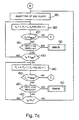
- a block 100 is reached in which, in a first register of the control circuit 92, there are stored the logic values (0 or 1) assumed by two flags F1 and F2, which for example are supplied by the engine control system (not shown).
- a control function of the electroinjectors 2 is implemented, which function comprises the LAUNCHING STEP, the BYPASS STEP, the first discharge step, the MAINTENANCE STEP and the SECOND DISCHARGE STEP previously described with reference to figures 3-6, in order to generate a current I L which has the development illustrated in figure 6; when both the flags F1 and F2 assume high logic values, a control function of the electroinjectors 2 is implemented which makes it possible to obtain in the LAUNCHING STEP alone a development of the current I L which flows in each electroinjector 2, which is slightly different from that illustrated in figure 6; whereas when both the flags F1 and F2 assume low logic values, a so-called "anti-rebound" control function of the electroinjectors 2 is implemented.
- condition in which the flag F1 assumes a low logic value and the flag F2 assumes a high logic value is an unused condition, to which no method for controlling the electroinjectors 2 corresponds.
- first and second series of binary DATA and ADDRESS data define the values of each of the time intervals referred to in the description of figures 3-6, i.e. they define in detail the duration of each of the sections which constitute the development of the current I L flowing in an electroinjector 2.
- a method for controlling HARDWARE or SOFTWARE which is to be implemented in the control device 1 (block 100) is also stored in a third register of the control circuit 92.
- the HARDWARE control method which can then optionally be modified during execution of the operations of the present control method.
- control device 1 can operate both in a HARDWARE control mode, in which the control circuit 92 uses the first reaction signal FBI in order to carry out a closed-loop check on the current I L flowing in the electroinjector 2, and uses the second and third reaction signals FBV1 and FBV2 to detect malfunctioning of the electroinjector 2, and it can operate in a SOFTWARE control mode, in which the control circuit 92 does not use the first reaction signal FBI, and carries out an open-loop check on the current I L flowing in the electroinjector 2, on the basis of the times stored in the second register of the control circuit 92 itself, and it uses only the second and third reaction signals FBV1 and FBV2 in order to detect malfunctioning of the electroinjector 2.
- piloting transistors 34 and 36 and the transfer transistor 78 are cut off, and act as open circuits.
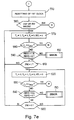
- block 140 it is verified whether there is present an edge of transition of the trigger signal TRG generated by the microprocessor 90 for the electroinjector 2, and which indicates the start of injection into the cylinder of the engine 6 with which the electroinjector 2 itself is associated.
- the operation carried out in block 170 starts the LAUNCHING STEP previously described with reference to figure 6, and in which there is generated a current which quickly increases to a value sufficient to command opening of the electroinjector 2.
- the hot side of the electroinjector 2 should be set to a positive voltage which is close to the voltage of the positive pole of the electrical energy source 16 (supply voltage) and the cold side should be set to a voltage which is close to the voltage of the negative pole of the electrical energy source 16 (earthing voltage)
- the second reaction signal FBV1 assumes a high logic level
- the third reaction signal FBV2 assumes a low logic level (YES output from block 180)
- there is correct functioning of the electroinjector 2 and thus from block 180 there is transition to a block 200
- the second reaction signal FBV1 assumes a low logic level
- the third reaction signal FBV2 assumes a high logic level (NO output from block 180)
- there is malfunctioning of the electroinjector 2 and thus from block 180 there is transition to block 150 for execution of the aforementioned method for detection of the type of malfunctioning.
- the state signal H/L is set to the high logic level, the first and second timing signals T 1 , T 2 are kept at the high logic level, and the timing signal T 3 is kept at the logic level assumed by F1, i.e. high.
- the state signal H/L set to a high logic level ensures that the comparator circuit 42 compares the voltage at the ends of the shunt resistor 38 with a high voltage value, thus supplying to the control circuit 92 a first reaction signal FBI which allows the control circuit 92 itself to carry out closed-loop control of the current I L which flows in the electroinjector 2, in order to maintain it around the average value I TH1 , as illustrated in figure 6.
- the hot side of the electroinjector 2 should be set to a positive voltage which is close to the supply voltage, and the cold side should be set to the earthing voltage, if the second reaction signal FBV1 assumes a high logic level and the third reaction signal FBV2 assumes a low logic level (YES output from block 230) then the electroinjector 2 is functioning correctly, and thus there is transition from block 230 to a block 250.
- HARDWARE mode If the HARDWARE mode is stored (HW output from block 270), then there is transition from block 270 to a block 280, otherwise, if the SOFTWARE mode is stored (SW output from block 270), then from block 270 there is transition to a block 380 for execution of alternative operations to those described hereinafter with reference to the HARDWARE mode.
- the third timing signal T 3 is set to a logic level which is the same as that assumed by the flag F2, which, as previously stated, in the example in question is a low logic level, whereas the first and second timing signals T 1 , T 2 and the state signal H/L are maintained at the high logic level.
- the operation described in block 280 starts the BYPASS STEP, in which, as previously stated, the current I L which flows in the electroinjector 2 assumes a sawtooth development around the average value I TH1 and between extreme values I 1 and I 2 , such as to command opening of the electroinjector 2.
- the combination of the logic levels of the timing signals T set in block 280 starts the rising section of a sawtooth of the current I L contained between I 1 and I 2 .
- the second reaction signal FBV1 assumes a high logic level
- the third reaction signal FBV2 assumes a low logic level (YES output from block 300)
- the second reaction signal FBV1 assumes a low logic level
- the third reaction signal FBV2 assumes a high logic level (NO output from block 300)
- there is malfunctioning of the electroinjector 2 for example because of a short-circuit to the earthing line 24, and thus from block 300 there is transition to block 150 for execution of the aforementioned method for detection of the type of malfunctioning.
- the first reaction signal FBI is obtained as a result of the comparison of the difference of voltage which is present at the ends of the shunt resistor 38, with the logic level of the state signal H/L, which in this step is high, and in fact represents the term of comparison defined by the threshold value I TH1 .
- the current I L has exceeded the threshold value I TH1 , and can start the descending section, and thus from block 320 there is transition to a block 330, otherwise, if the first reaction signal FBI is at the low logic level (NO output from block 320), then the current I L has not yet exceeded the threshold value I TH1 , and therefore from block 320 there is transition to block 280 once more.
- the second and third reaction signals FBV1 are both at the low logic level (YES output from block 350), then there is correct functioning of the electroinjector 2, and thus from block 350 there is transition to a block 370, otherwise, if at least one of the second and third reaction signals FBV1, FBV2 is at the high logic level (NO output from block 350), then there is malfunctioning of the electroinjector 2, for example because of a short-circuit to the supply line 22, and therefore from block 350 there is transition to block 150 for execution of the aforementioned method for detection of the type of malfunctioning.
- the current I L has crossed the threshold value I TH1 , and is therefore smaller than the threshold value I TH1 , and thus from block 370 there is transition once more to block 280, to start the rising section of a subsequent sawtooth, otherwise, if the first reaction signal FBI is at the high logic level (NO output from block 370), then the current I L has not yet crossed the threshold value I TH1 , and the threshold value I TH1 is thus still greater, and therefore from block 370 there is transition once more to block 330.
- the operation carried out in block 390 starts the BYPASS STEP illustrated in figure 6, and in particular the combination of the logic levels of the timing signals T set in block 280 starts the rising section of the sawtooth of the current I L which is contained between I 1 and I 2 and has the duration t ONH .
- time t B is longer than, or the same as the time t BYPASS (YES output from block 400), then from block 400 there is transition to block 500, otherwise, if the time t B is shorter than the time t BYPASS (NO output from block 400), then from block 400 there is transition to a block 410.
- the first timing signal T 1 is set to the low logic level, whereas the second timing signal T 2 and the state signal H/L are maintained at the high logic level, and the third timing signal T 3 is maintained at the low logic level assumed by the flag F2, thus starting the descending section of the current I L which is contained between I 2 and I 1 , and has the duration t OFFH .
- block 950 it is chosen to disable the malfunctioning electroinjector 2 (DISABLING output), then from block 950 there is transition to a block 995 in which disabling of the malfunctioning electroinjector 2 is indicated.
- the development of the current I L is similar to that illustrated in figure 6, and differs from the latter only during the LAUNCHING STEP, in particular in that it has a sawtooth development with ascending sections with a greater slope than that of the ascending sections in figure 6.
- timing signal T 3 is not switched to the low logic level, but is maintained at the high logic level also for the time t BYPASS , thus keeping the transistor 78 closed also during the BYPASS STEP.
- the supply line 22 is maintained at the voltage V C generated by the voltage-increasing circuit 32 also during the BYPASS STEP, and thus during the time intervals t ONH of this step, the current which flows in the electroinjector 2 increases substantially linearly with a slope equivalent to V C /L, which is greater than the slope V B /L with which it increases if the transistor 78 is closed on completion of the LAUNCHING STEP.
- the first and second series of binary DATA and ADDRESS data which are supplied by the microprocessor 90, and which indicate the duration of the intervals of activation of the piloting transistors 34 and 36 and of the transfer transistor 78 of the piloting circuit 10, will be different from those relating to the operative methods described with reference to figures 3-6, in the part which relates to the value of the time t 1 and the time t ONH .
- control of the electroinjectors comprises only the LAUNCHING STEP, the BYPASS STEP, and the FIRST DISCHARGE STEP, whereas the MAINTENANCE STEP and the SECOND DISCHARGE STEP are not carried out.
- the supply line 22 is maintained constantly at the voltage V B supplied by the electrical energy source 16, and thus both during the LAUNCHING STEP and during the time intervals t ONH of the successive BYPASS STEP, the current I L which flows in the electroinjector 2 increases substantially linearly with a slope equivalent to V B /L, in which V B is the voltage supplied by the electrical energy source 16, which is smaller than the slope V C /L with which it increases if the transistor 78 is closed during the LAUNCHING STEP.
- the current I L which flows in the electroinjector 2 during the LAUNCHING STEP increases to a value which is substantially the same as the value I4 assumed by the current I L during the MAINTENANCE STEP illustrated in figure 6, whereas in the BYPASS STEP it has a sawtooth development which oscillates between values which are substantially the same as the values I5 and I6 assumed by the current I L during the MAINTENANCE STEP illustrated in figure 6.
- the first and second series of binary DATA and ADDRESS data supplied by the microprocessor 90 and which indicate the duration of the intervals of activation of the piloting transistors 34 and 36 and of the transfer transistor 78 of the piloting circuit 10, will be different from those relative to the operating methods described with reference to figures 3-6, both in the part relating to the value of the times t 1 , t ONH and t BYPASS , and in the part relating to the times t ONL , t HOLD and t 3 .
- an electroinjector comprises an outer body which defines a cavity which communicates with the exterior by means of an injection nozzle, and in which there is accommodated a small rod loaded by a spring, which is mobile between a position of opening and a position of closing of the nozzle, and is normally maintained electromagnetically in the opening position, against the action of the spring.
- the invention permits choice between a HARDWARE control mode and a SOFTWARE control mode for the control device 1, thus making it possible to carry out closed-loop control, by monitoring the current flowing in the electroinjectors 2, or open-loop control of the piloting device 10.
- the piloting device 10 could comprise a plurality of voltage-increasing circuits 32, each of which is connected to a respective control circuit 30, or to a respective group of control circuits 30, thus increasing further the versatility of use of the control device 1 itself, or it could comprise a single voltage-increasing circuit 32 which cooperates with a plurality of control circuits 30, by means of respective transistors 78 which are controlled independently from one another.
- the piloting device 10 comprises a plurality of voltage-increasing circuits 32, to each of which there is connected a group of control circuits 30 (or at least a single control circuit 30), the connection between each voltage-increasing circuit 32 and the corresponding control circuits 30 (or the corresponding control circuit 30), as well as the functioning of the latter, is altogether identical to that previously described with reference to figure 2, and is thus not described again.
- circuit structure of the piloting device 10 can be simplified in all cases in which the specific structure of the electroactuator used requires a control current which has a development such that the LAUNCHING STEP can be carried out simply by means of the voltage supplied by the electrical energy source 16.
- the voltage-increasing circuit 32 can be eliminated, since its purpose is in fact to supply a voltage value which is greater than the voltage supplied by the electrical energy source 16, in order to carry out a LAUNCHING STEP in which the control current of the electroactuator 2 increases very rapidly to the value I 1 in the time t 1 , which depends both on the electrical characteristics of the electroactuator 2 and on the temporal resolution specifications required.
- the supply line 22 is connected directly to the first input terminal 12, and the discharge of the electroinjector 2 caused by simultaneous opening of the piloting transistor 34 and of the piloting transistor 36, which previously took place in the loop comprising the recirculation diode 89 and the capacitor 88, now takes place via the parasitic diodes associated with the body area (body diode) of the piloting transistors 34, 36 themselves.
- control circuits 30 could be connected to a single shunt resistor 38, and in this case the control circuit 92 would receive as input a single first reaction signal FBI.
Landscapes
- Engineering & Computer Science (AREA)
- Mechanical Engineering (AREA)
- Physics & Mathematics (AREA)
- General Physics & Mathematics (AREA)
- Radar, Positioning & Navigation (AREA)
- Automation & Control Theory (AREA)
- Chemical & Material Sciences (AREA)
- Electromagnetism (AREA)
- General Engineering & Computer Science (AREA)
- Combustion & Propulsion (AREA)
- Electronic Switches (AREA)
- Electrical Control Of Air Or Fuel Supplied To Internal-Combustion Engine (AREA)
- Fuel-Injection Apparatus (AREA)
- Vehicle Body Suspensions (AREA)
- Fluid-Damping Devices (AREA)
- Programmable Controllers (AREA)
Abstract
Description
- The present invention relates to an electroactuator control device and to a method for controlling this control device.
- The control device according to the present invention can be used advantageously, but need not be used exclusively, to control electroinjectors of an injection system for an internal combustion engine of the petrol, diesel, methane or LPG-operated type, to which the following description will make specific reference, without however detracting from general applicability.
- In fact the control device according to the present invention can also be applied to any other type of electroactuator, such as solenoid valves of ABS devices and the like, and solenoid valves of variable phasing systems etc.
- As is known, in order to control the electroinjectors of an injection system of an internal combustion engine, it is necessary to supply to each electroinjector a current, the development of which over a period of time comprises a section of fast increase, a section of slower increase, a section of decrease to a maintenance value, a section of oscillating amplitude around the maintenance value, and a section of decrease to a value of approximately zero.
- In order to obtain this development over a period of time, at present control devices are used in which the electroinjectors are connected on the one hand to a low voltage supply source, and on the other hand to an earthing line, by means of a controlled electronic switch.
- These control devices have the disadvantage that any short-circuit to earth of one of the terminals of any of the electroinjectors, caused for example by a loss of insulation in a wiring conductor of the electroinjectors themselves, and by the contact of this conductor with the vehicle bodywork, would damage definitively the electroinjector itself and/or the control device, thus making the vehicle stall, which is a decidedly dangerous situation when the vehicle is running.
- In order to avoid this dangerous disadvantage, control devices for electroinjectors have been proposed which are connected on the one hand to earth, and on the other hand to an internal node of the control devices themselves, such that any short-circuit to earth of one of the terminals of the electroinjectors does not give rise to damage to the control device, and thus to stalling of the vehicle, but simply puts that individual electroinjector out of use, so that the vehicle can continue to run with one electroinjector short.
- However these control devices have the disadvantage that their circuitry is complicated, they are costly, and also in general they do not make it possible to carry out simultaneous injections into different cylinders, which would however be necessary for example in cases in which control of injection of the engine requires multiple injections into each cylinder.
- The object of the present invention is to produce an electroactuator control device which is simple, economical, and makes it possible to eliminate the above-described disadvantages.
- According to the present invention, an electroactuator control device is provided, as described in
claim 1. - The present invention also relates to a method for controlling this control device, as described in claim 23.
- In order to assist understanding of the present invention, a preferred embodiment is now described, purely by way of non-limiting example, and with reference to the attached drawings, in which:
- figure 1 is a block diagram of an injection system of an internal combustion engine comprising a control device according to the present invention;
- figure 2 is a circuit diagram of the control device in figure 1;
- figures 3-6 show developments over a period of time of quantities relating to the control device in figure 2;
- figures 7a-7h show a flow chart relating to the control method which is the subject of the present invention; and
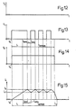
- figures 8-15 show development over a period of time of quantities relating to the control device in figure 2.
- In figure 1, 1 indicates as a whole a control device for
electroinjectors 2 of aninjection system 4 of an internal combustion engine 6 of a vehicle (not shown). In particular, theelectroinjectors 2 are illustrated by means of electrical equivalents consisting of inductors. - The
control device 1 comprises atiming circuit 8 which receives as input data signals S which are measured on the engine 6, in particular speed and angular position of the engine 6 and injection advance, and which generates as output timing signals T and state signals H/L which are used to control theelectroinjectors 2; it also comprises apiloting circuit 10 which receives as input the timing signals T and the state signals H/L, and has the function of piloting theelectroinjectors 2 on the basis of the timing signals T and of the state signals H/L, as well as of generating reaction signals FBI, FBV1 and FBV2 for thetiming circuit 8, in the manner described in greater detail hereinafter. - As shown in figure 2, the
piloting circuit 10 comprises a first and asecond input terminal 12, 14, which can be connected respectively to a positive pole and a negative pole of anelectrical energy source 16, for example a battery of the vehicle, and a plurality of pairs of output terminals, one for eachelectroinjector 2, each of which comprises a first and asecond output terminal respective electroinjector 2 is connected in use. - The
piloting circuit 10 additionally comprises asupply line 22, which is connected in the manner described in greater detail hereinafter to thefirst input terminal 12; anearthing line 24 which is directly connected to the second input terminal 14 and to the electrical earth of the vehicle; and aninternal connection line 26. - The
piloting circuit 10 additionally comprises a plurality ofcircuits 30 for controlling theelectroinjectors 2, one for eachelectroinjector 2, connected to the supply andearthing lines timing circuit 8, and each interposed between the first and thesecond input terminal 12, 14 and a respective pair ofoutput terminals respective electroactuators 2. - The
piloting circuit 10 additionally comprises a voltage-increasingcircuit 32 which is common to thecontrol circuits 30, and is connected to the supply andearthing lines connection line 26, to thecontrol circuits 30, with the purpose of supplying a higher voltage than the voltage supplied by theelectrical energy source 16, in order, in the initial control step of theelectroactuators 2, to permit generation of a current which increases substantially linearly, with a slope which is greater than the slope which can be obtained by means of the voltage supplied by theelectrical energy source 16, and co-operating with thecontrol circuit 30 which in each case is activated in order to supply thecorresponding electroinjector 2. - Each
control circuit 30 comprises afirst piloting transistor 34 of the MOSFET type, which has a control terminal connected to thetiming circuit 8, and receives from the latter a first timing signal T1, a sink terminal which is connected to thesupply line 22, and a source terminal which is connected to thefirst output terminal 18; and asecond piloting transistor 36 of the MOSFET type, which has a control terminal connected to thetiming circuit 8, and receives from the latter a second timing signal T2, a sink terminal which is connected to thesecond output terminal 20, and a source terminal which is connected to theearthing line 24 by means of ashunt resistor 38. - Each
control circuit 30 also comprises adischarge diode 40, the anode of which is connected to theearthing line 24, and the cathode of which is connected to thefirst output terminal 18. - Each
control circuit 30 also comprises acomparator circuit 42, which has afirst input terminal 44 connected to the source terminal of thesecond piloting transistor 36, i.e. which is connected to a terminal of theshunt resistor 38, asecond input terminal 46 which is connected to thetiming circuit 8 and receives from the latter a state signal H/L, and anoutput terminal 48 to which it supplies a first reaction signal FBI which is supplied to thetiming circuit 8 itself. - The state signal H/L is a digital-type voltage signal, and assumes a high logic level which is defined by a first voltage value, for example 5 volts, and a low logic level which is defined by a second voltage value which is lower than the first, for example 0 volt. The state signal H/L switches from the high logic level to the low logic level during control of the
corresponding electroinjector 2, in the manner described in greater detail hereinafter. - The
comparator circuit 42 has the purpose of comparing the voltage of the source terminal of thepiloting transistor 36, relative to the voltage of theearthing line 24, with the voltage value assumed by the state signal H/L, in order to generate the first reaction signal FBI according to the result of the comparison. - In detail, the first reaction signal FBI is a digital-type voltage signal which indicates whether or not current is passing in the
corresponding electroinjector 2, and assumes a first logic level, for example the high logic level, when the voltage at the ends of theshunt resistor 38 is greater than the voltage value assumed by the first state signal H/L (i.e. when current is passing in the corresponding electroinjector 2), and it assumes a second logic level, the low logic level in the example in question, when the voltage at the ends of theshunt resistor 38 is the same as, or lower than the voltage value assumed by the first state signal H/L (i.e. when current is not passing in the corresponding electroinjector 2). - The first reaction signal FBI is used by the
timing circuit 8 in order to carry out a closed-loop check on the current which is flowing in thecorresponding electroinjector 2, in the manner described in detail hereinafter. - Each
control circuit 30 additionally comprises a first voltage-limitingcircuit 52 which has aninput terminal 54 which is connected to the source terminal of thefirst piloting transistor 34, i.e. which is connected to thefirst output terminal 18 of thecontrol circuit 30 itself, and anoutput terminal 56 to which it supplies a second reaction signal FBV1, which is supplied to thetiming circuit 8. - The first voltage-limiting
circuit 52 has the purpose of supplying to the output terminal 56 a second reaction signal FBV1, which is obtained by limiting the dynamics of the voltage of the source terminal of thefirst piloting transistor 34, which is typically variable between 0 and 12 volts. In particular, the second reaction signal FBV1 is a voltage signal substantially of the digital type, which is indicative of the voltage value assumed by the so-called "hot side" of thecorresponding electroinjector 2, and assumes a high logic level which is defined by the first voltage value, for example 5 volts, when the hot side of thecorresponding electroinjector 2 is set to a voltage which is close to the voltage of the positive pole of theelectrical energy source 16, and it assumes a low logic value which is defined by a second voltage value lower than the first, for example 0 volt, when the hot side of thecorresponding electroinjector 2 is set to a voltage which is close to the voltage of the negative pole of the electrical energy source 16 (earthing voltage). - Each
control circuit 30 additionally comprises a second voltage-limitingcircuit 62 which has aninput terminal 64 connected to the sink terminal of thesecond piloting transistor 36, i.e. which is connected to thesecond output terminal 18 of thecontrol circuit 30 itself, and anoutput terminal 66 to which it supplies a third reaction signal FBV2 which is supplied to thetiming circuit 8. - The second voltage-limiting
circuit 62 has the purpose of supplying to the output terminal 66 a third reaction signal FBV2 which is obtained by limiting the dynamics of the voltage of the sink terminal of thesecond piloting transistor 36, which is typically variable between 0 and 12 volts. In particular, the third reaction signal FBV2 is a voltage signal substantially of the digital type, which is indicative of the voltage value present at the so-called "cold side" of thecorresponding electroinjector 2, and assumes a high logic level which is defined by a first voltage value, for example 5 volts, when the cold side of theelectroinjector 2 is set to a voltage which is close to the voltage of the positive pole of theelectrical energy source 16, and it assumes a low logic value which is defined by a second voltage value lower than the first, for example 0 volt, when the cold side of theelectroinjector 2 is set to a voltage which is close to the voltage of the negative pole of the electrical energy source 16 (earthing voltage). - The second and third reaction signals FBV1 and FBV2 are used by the
timing circuit 8 in order to carry out monitoring of the malfunctioning of thecorresponding electroinjector 2, in the manner described in detail hereinafter. - The voltage-increasing
circuit 32 comprises a load diode 70 (shown outside the voltage-increasingcircuit 32 purely for reasons of convenience of representation), which is interposed between thefirst input terminal 12 of thepiloting circuit 10 and thesupply line 22, and which in particular has the anode connected to thefirst input terminal 12 and the cathode connected to thesupply line 22; avoltage converter 72 of the DC/DC type (switching converter of the direct current/direct current type, to increase the input voltage), for generation of a voltage which is greater than that supplied by theelectrical energy source 16, with aninput terminal 74 connected to thefirst input terminal 12, afirst output terminal 76 connected to thesupply line 22 via atransfer transistor 78, and asecond output terminal 80 connected to theearthing line 24. - In particular, the
load diode 70 defines a controlled switch which permits selective connection between thesupply line 22 and thefirst input terminal 12 of thepiloting circuit 10, on the basis of the voltage value present at the ends of theload diode 70 itself. - The
transfer transistor 78 is a MOSFET transistor which has a control terminal connected to thetiming circuit 8, and receives from the latter a third timing signal T3, a sink terminal connected to thefirst output terminal 76 of thevoltage converter 72, and a source terminal connected to thesupply line 22. - The
voltage converter 72, which is of a known type and is therefore not described in detail, substantially comprises aninductor 82 which has a first terminal connected to thefirst input terminal 74, and a second terminal connected to the anode of atransfer diode 84, the cathode of which is connected to thefirst output terminal 76. - The
voltage converter 72 additionally comprises aload transistor 86 of the MOSFET type with a control terminal which receives (from a controller which is of a known type and is not illustrated) a control signal for piloting of theload transistor 86 itself in the event of saturation or cut-off, a sink terminal which is connected to the anode of thetransfer diode 84, and a source terminal which is connected to theearthing line 24. - The
high voltage circuit 32 additionally comprises acapacitor 88 which has a first and a second terminal connected respectively to thefirst output terminal 76 of thevoltage converter 72 and to theearthing line 24. - The voltage-increasing
circuit 32 additionally comprises a plurality ofrecirculation diodes 89, one for each control circuit 30 (shown outside the voltage-increasingcircuit 32 purely for reasons of convenience of representation), which has the anodes connected to respectivesecond output terminals 20 of thepiloting circuit 10, and the cathodes connected to thefirst output terminal 76 of thevoltage converter 72. - With reference once again to figure 1, the
timing circuit 8 comprises amicroprocessor 90 which receives as input the data signals S measured on the engine 6, and which, on the basis of the data signals S, generates as output operative data for control of theinjectors 2; and acontrol circuit 92 which is connected at its input to themicroprocessor 90, and which, in addition to the operative data supplied by themicroprocessor 90 itself, receives the first, the second and third reaction signals FBI, FBV1 and FBV2 generated by thepiloting circuit 10, and generates as output, on the basis of the said operating data and the reaction signals FBI, FBV1 and FBV2, the timing signals T for thepiloting circuit 10 itself, thus implementing the control method which is the subject of the present invention. - The
control circuit 92 also generates as output an interrupt signal INT which is supplied to themicroprocessor 90 in order to interrupt its operations in particular operating situations, as described in greater detail hereinafter. - In particular, in a known manner, on the basis of data signals S, the
microprocessor 90 generates as output a first and second series of binary data i.e. DATA, ADDRESS, which indicates the temporal duration of the intervals of activation of thepiloting transistors transfer transistor 78 of thepiloting circuit 10, which data is supplied to thecontrol circuit 92 via data BUS lines. - The
microprocessor 90 also generates as output trigger signals TRG of the pulse type, which are supplied to thecontrol circuit 92, and have a (rising or descending) edge which indicates the start of injection into each cylinder of the engine 6. - The
timing circuit 8 generates as output a number of first and second timing signals T1, T2 equivalent to the number ofcontrol circuits 30 which are connected to thesupercharging circuit 32, i.e. equivalent to the number ofelectroinjectors 2 contained in a so-called "set", a third timing signal T3 for each set ofelectroinjectors 2, and a state signal H/L for each set ofelectroinjectors 2, whereas it receives as input a number of first, second and third reaction signals FBI, FBV1 and FBV2 equivalent to the number ofcontrol circuits 30 connected to thesupercharging circuits 32. - The
timing circuit 8 activates eachcontrol circuit 30 selectively by supplying the timing signals T1, T2, T3 to the control terminals of thecorresponding piloting transistors transfer transistor 78 of the voltage-increasingcircuit 32. - The timing signals T1, T2, T3 are digital-type voltage signals and assume a high logic level, i.e. a
logic level 1, for example of 5 volts, and a low logic level, i.e. alogic level 0, for example of 0 volt, in order to control thepiloting transistors transfer transistor 78 respectively in the event of saturation and cut-off; each transistor therefore acts as an open or closed switch. - The timing signals T1, T2, T3 are supplied in each case only to the
control circuit 30 of theelectroinjector 2 to be piloted, or to thecontrol circuits 30 of theelectroinjectors 2 to be piloted, and are not supplied to theother control circuits 30, which are therefore inactive. - The functioning of the
control device 1 will now be described with reference to piloting of a single one of theelectroinjectors 2, and thus the functioning will be described of a single one of thecontrol circuits 30, which cooperates with the voltage-increasingcircuit 32 for supply of thecorresponding electroinjector 2. - The description for the
other control circuits 30 is altogether similar, and therefore it will not be repeated. - Additionally, the description of the functioning of the
control circuit 30 will refer to figures 3-6, which illustrate the development over a period of time of the timing signals T1, T2, T3 of thepiloting transistors transfer transistor 78, as well as of the current IL which flows in theelectroinjector 2. - There will then be described the method for controlling the
piloting circuit 10 which is implemented by thetiming circuit 8, and in particular by thecontrol circuit 92. - As illustrated in figures 3-6, initially, before the start of any operation for controlling the
electroinjector 2, thevoltage converter 72 loads thecapacitor 88 in a known manner such that at its ends there is present a voltage VC which is greater than the voltage VB supplied by theelectrical energy source 16. - In particular, in order to carry out the said loading on the control terminal of the
load transistor 86, a set of pulses is supplied in order to command repeatedly closing and opening of theload transistor 86 itself, thus giving rise to a progressive increase to a pre-determined value of the voltage at the ends of thecapacitor 88, such as to permit subsequent piloting of theelectroinjector 2. - In fact, when the
load transistor 86 is closed, a closed loop is formed, comprising theinductor 82, theload transistor 86 and theelectrical energy source 16. Since theinductor 82 is supplied with a constant voltage by theelectrical energy source 16, an increasing current passes through it, which gives rise to an increase in the energy accumulated in theinductor 82 itself. - When the
load transistor 86 is opened, the current in the aforementioned loop is interrupted, and thus the storage of energy in theinductor 82 is interrupted. - After the
load transistor 86 has been opened, thecapacitor 88 and theinductor 82 are connected to one another in series via thetransfer diode 84, and thus current flows in the loop defined by theinductor 82, thetransfer diode 84 and thecapacitor 88, which loads thecapacitor 88 and gives rise to an increase in the voltage at its ends. - Thus, unless there are leakages, the energy which is stored in the
inductor 82 is transferred to thecapacitor 88. - The continual repetition of closing and opening of the
transfer transistor 78 thus gives rise to a gradual increase in the voltage at the ends of thecapacitor 88. - When the step of loading the
capacitor 88 has been completed, thetiming circuit 8 commands opening of the pilotingtransistors transfer transistor 78, and thus thecontrol circuit 30 is inactive, and there is no electrical connection between the voltage-increasingcircuit 32 and thesupply line 22. - Subsequently, the
timing circuit 8 initially commands closing of the pilotingtransistors discharge transistor 78, for a pre-determined interval of time, indicated as t1 in figures 3 and 6, and starting from an instant of time indicated as t0, thus starting the so-called "LAUNCHING STEP", in which there is generated a current which increases rapidly over a period of time, up to a value which is sufficient to command opening of theelectroinjector 2. - In particular, during the LAUNCHING STEP, the
transfer transistor 78 connects thesupply line 22 to the first terminal of thecapacitor 88, thus determining the existence of a difference in voltage between thesupply line 22 itself and the earthingline 24, which difference is equivalent to the voltage VC which exists at the ends of thecapacitor 88. - In addition, closing of the piloting
transistors capacitor 88, theelectroinjector 2 and the pilotingtransistors capacitor 88. - Simultaneously, the
capacitor 88 is kept loaded with the voltage VC by thevoltage converter 72, in the manner previously described. - As shown in figure 6, during the LAUNCHING STEP the current IL which flows in the
electroinjector 2 increases substantially linearly, with a slope which is equivalent to VC/L, in which L is the equivalent inductance of theelectroinjector 2 and VC is the voltage at the ends of the capacitor, up to a value I1 which is equivalent to VC*t1/L, such as to command instantaneous opening of theelectroinjector 2 itself. - It should be noted that the value I1 of the current which flows in the
electroinjector 2 during the LAUNCHING STEP, and thus the first average value ITH1 around which the current oscillates during this step, depends on the value of the voltage VC at the ends of thecapacitor 88; thus the value of the voltage VC is typically determined a priori (and is obtained by controlling thevoltage converter 72 accordingly), according to the current value to be obtained during the LAUNCHING STEP, in order to command closing of theelectroinjector 2. - On completion of the LAUNCHING STEP, the
timing circuit 8 commands opening of thetransfer transistor 78, thus determining interruption of the connection between thesupply line 22 and thecapacitor 88, and the start of the so-called "BYPASS STEP", in which the current which flows in theelectroinjector 2 is maintained around an average value, such as to command opening of theelectroinjector 2. - In particular, during the BYPASS STEP, the
timing circuit 8 commands closing and opening of the pilotingtransistor 34 repeatedly, and for a pre-determined time interval which is indicated as tBYPASS in figures 4 and 6, such that the current which flows in theelectroinjector 2 assumes a sawtooth development which has a duration tp, and oscillates around a first average pre-determined value, for example 20 A, which is indicated as ITH1 in figure 6. - In particular, when the
connection transistor 78 is opened, since the pilotingtransistor 34 is closed, thetiming circuit 8 continues to keep the latter closed for a pre-determined time interval, which is indicated as tONH in figures 4 and 6. - By this means, during the time interval tONH, the current continues to reach the
electroinjector 2, by flowing in the loop which comprises theelectrical energy source 16, theload diode 70, theelectroinjector 2, and the pilotingtransistors - In particular, during the time interval tONH, the
electrical energy source 16 supplies a constant voltage to theelectroinjector 2, through which there therefore passes an increasing current which keeps the electroinjector open. - As shown in figure 6, the current which flows in the
electroinjector 2 continues to increase, but with a slope which is lesser than the slope obtained in the launching step. - In particular, during the time interval tONH, the current which flows in the
electroinjector 2 increases substantially linearly, with a slope which is equivalent to VB/L, in which VB is the voltage supplied by theelectrical energy source 16, up to a value I2 which is equivalent to I1+VB*tONH/L. - After the time interval tONH, the
timing circuit 8 commands opening of the pilotingtransistor 34 for a pre-determined time interval indicated as tOFFH in figures 4 and 6, and current derived from the energy stored in theelectroinjector 2 flows in the loop which comprises thedischarge diode 40, the pilotingtransistor 36 and theelectroinjector 2. - In particular, during the time interval tOFFH, the
electroinjector 2 is discharged in the said loop, and the current which flows in the electroinjector decreases substantially linearly, with a slope which is equivalent to VD/L, in which VD is the voltage present at the ends of theelectroinjector 2, up to a value I3 which is equivalent to I2-VD*tOFFH/L, and is approximately equal to I1. - Thus, repetition of closing and opening of the piloting
transistor 34 provides a current IL which flows in theelectroinjector 2 with the sawtooth development which has a duration tp, which is obviously equivalent to the sum of the times tONH and tOFFH, and oscillates around the first average value ITH1 illustrated in figure 6. - On completion of the BYPASS STEP, with the piloting
transistor 34 open, for a pre-determined time interval indicated as t2 in figures 5 and 6, thetiming circuit 8 also commands opening of the pilotingtransistor 36, thus starting the so-called "FIRST DISCHARGE STEP", in which the current IL decreases substantially linearly. - In particular, when the piloting
transistor 36 is also opened, a loop is formed which comprises thecapacitor 88, theelectroinjector 2, there-circulation diode 89 and thedischarge diode 40, and theelectrodiode 2 is discharged in this loop. - The discharge current of the
electroinjector 2 thus loads thecapacitor 88, and the voltage at its ends increases. - As shown in figure 6, during discharge of the
electroinjector 2, the current which flows in it decreases substantially linearly, with a slope which is equivalent to VC/L, up to a value I4 equivalent to I3-VC*t2/L. - After the time interval t2, the FIRST DISCHARGE STEP is completed, and the
timing circuit 8 commands closing of the pilotingtransistor 36, and repeatedly, for a pre-determined time interval which is indicated as tHOLD in figures 4 and 6, it commands closing and opening of the pilotingtransistor 34, thus giving rise to the start of the so-called "MAINTENANCE STEP", in which the current which flows in theelectroinjector 2 is maintained around an average value which is sufficient to keep theelectroinjector 2 open. - In particular, the MAINTENANCE STEP is substantially similar to the preceding BYPASS STEP, with the difference however that the current which flows in the
electroinjector 2 assumes a sawtooth development which oscillates around a second, pre-determined average value which is lower than the first average value, for example 10 A, indicated as ITH2 in figure 6, which is sufficient to keep theelectroinjector 2 open. - In detail, during the MAINTENANCE STEP, and after closing of the piloting
transistor 36, thetiming circuit 8 commands opening of the pilotingtransistor 34 for a pre-determined time interval, which is indicated as tONL in figures 4 and 6, and the current reaches theelectroinjector 2, and flows, similarly to the process during the BYPASS STEP, in the loop which comprises theelectrical energy source 16, theload diode 70, theelectroinjector 2 itself, and the pilotingtransistors - During the time interval tONL, an increasing current passes through the
electroinjector 2, in a substantially linear manner, with a slope which is equivalent to VB/L, up to a value I5 which is equivalent to I4+VB*tONL/L. - It should be noted that the value Is of the current which flows in the
electroinjector 2 during the MAINTENANCE STEP, and thus the second average value ITH2 around which the current oscillates during this step, depends on the value of the voltage VB supplied by theelectrical energy source 16, and no longer on the voltage VC at the ends of thecapacitor 88. - After the time interval tONL, the
timing circuit 8 commands opening of the pilotingtransistor 34 for a pre-determined time interval which is indicated as tOFFL in figures 4 and 6, and similarly to the process during the BYPASS STEP, a current derived from the energy stored in theelectroinjector 2 flows in the loop which comprises thedischarge diode 40, the pilotingtransistor 36 and theelectroinjector 2. - During the time interval tOFFH, the
electroinjector 2 is discharged in the said loop, and the current which flows in it decreases substantially linearly with a slope equivalent to VD/L, to a value I6 which is equivalent to I5-VD*tOFFL/L, and is approximately equivalent to I4. - Thus, by repeating the closing and opening of the piloting
transistor 34, a current IL flowing in theelectroinjector 2 is obtained, which current has the oscillating sawtooth development around the second average value ITH2 illustrated in figure 6. - On completion of the MAINTENANCE STEP, the
timing circuit 8 commands opening of the pilotingtransistors electroinjector 2 decreases substantially linearly. - In particular, after the piloting
transistors electroinjector 2 is discharged in the loop which comprises thecapacitor 88, theelectroinjector 2 itself, therecirculation diode 89 and thedischarge diode 40. - During discharge of the
electroinjector 2, which takes place for a time interval indicated as t3 in figure 6, the current which flows in the electroinjector decreases substantially linearly, with a slope equivalent to VC/L, to a value of substantially zero. - When the time t3 has elapsed since the piloting
transistors timing circuit 8 can start a new piloting cycle of anotherelectroinjector 2, repeating the operations previously described. - Examination of the characteristics of the
control device 1 according to the present invention makes apparent the advantages which can be obtained by means of the invention. - Firstly, the fact that each
electroinjector 2 is not connected directly either to the supply voltage or to earth means that any short-circuit to earth or to the supply voltage of one of the terminals of anelectroinjector 2, does not cause damage either to theelectroinjector 2 itself or to thecontrol device 1, but simply gives rise to exclusion of thiselectroinjector 2, without affecting the functioning of theother electroinjectors 2, and thus without making the vehicle stall suddenly. - Furthermore, since the
voltage converter 72 keeps thecapacitor 88 constantly loaded, by means of thecontrol device 1 it is possible to pilotseveral injectors 2 simultaneously, in order to carry out for example either successive injections into each cylinder, or simultaneous injections into several cylinders. - Finally, the
control device 1 has a circuit structure which is decidedly simplified compared with that of the known control devices. - In order to obtain the above-described functioning of the piloting
circuit 10, thecontrol circuit 92 implements the operations described hereinafter with reference to figures 7a-7h, and relative to the control method which is the subject of the present invention. - Similarly to the description given for functioning of the piloting
circuit 10, the control method implemented by thecontrol circuit 92 will now be described with reference to piloting of a single one of theelectroinjectors 2. - As illustrated in figures 7a-7h, initially a
block 100 is reached in which, in a first register of thecontrol circuit 92, there are stored the logic values (0 or 1) assumed by two flags F1 and F2, which for example are supplied by the engine control system (not shown). - In particular, to three of the possible combinations of the logic values assumed by the flags F1 and F2, there correspond respective control functions of the
electroinjectors 2, which are implemented by thecontrol circuit 92, and for each of these functions themicroprocessor 90 generates respective binary DATA and ADDRESS data, whereas no control function corresponds to a fourth combination of the logic values assumed by the flags F1 and F2. - In detail, when the flag F1 assumes a high logic value (logic value 1) and the flag F2 assumes a low logic value (logic value 0), a control function of the
electroinjectors 2 is implemented, which function comprises the LAUNCHING STEP, the BYPASS STEP, the first discharge step, the MAINTENANCE STEP and the SECOND DISCHARGE STEP previously described with reference to figures 3-6, in order to generate a current IL which has the development illustrated in figure 6; when both the flags F1 and F2 assume high logic values, a control function of theelectroinjectors 2 is implemented which makes it possible to obtain in the LAUNCHING STEP alone a development of the current IL which flows in eachelectroinjector 2, which is slightly different from that illustrated in figure 6; whereas when both the flags F1 and F2 assume low logic values, a so-called "anti-rebound" control function of theelectroinjectors 2 is implemented. - However, on the other hand, the condition in which the flag F1 assumes a low logic value and the flag F2 assumes a high logic value is an unused condition, to which no method for controlling the
electroinjectors 2 corresponds. - The control method described with reference to figures 7a-7h will be described with reference initially to the method for controlling the
electroinjectors 2 illustrated in figures 3-6, i.e. with reference to the condition in which the flags F1 and F2 assume respectively a high and a low logic value. Subsequently, the control methods which can be obtained when the flags F1 and F2 assume the other logic values will be described. - With reference to the function for controlling the
electroinjectors 2 which is illustrated in figures 3-6, after storage of the logic values assumed by the flags F1 and F2, there is storage in a second register of thecontrol circuit 92, of the first and second series of binary DATA and ADDRESS data supplied by themicroprocessor 90, and which indicate the duration of the intervals of activation of the pilotingtransistors transfer transistor 78 of the piloting circuit 10 (block 100). - In particular, the first and second series of binary DATA and ADDRESS data define the values of each of the time intervals referred to in the description of figures 3-6, i.e. they define in detail the duration of each of the sections which constitute the development of the current IL flowing in an
electroinjector 2. - Subsequently, a method for controlling HARDWARE or SOFTWARE, which is to be implemented in the control device 1 (block 100) is also stored in a third register of the
control circuit 92. In particular, when the present method is first executed, there is stored in the third register the HARDWARE control method, which can then optionally be modified during execution of the operations of the present control method. - In fact, the
control device 1 can operate both in a HARDWARE control mode, in which thecontrol circuit 92 uses the first reaction signal FBI in order to carry out a closed-loop check on the current IL flowing in theelectroinjector 2, and uses the second and third reaction signals FBV1 and FBV2 to detect malfunctioning of theelectroinjector 2, and it can operate in a SOFTWARE control mode, in which thecontrol circuit 92 does not use the first reaction signal FBI, and carries out an open-loop check on the current IL flowing in theelectroinjector 2, on the basis of the times stored in the second register of thecontrol circuit 92 itself, and it uses only the second and third reaction signals FBV1 and FBV2 in order to detect malfunctioning of theelectroinjector 2. - From
block 100, there is then transition to a block 110 in which the first, second and third timing signals T1, T2, T3 and the state signal H/L are set to the low logic level. - By this means the piloting
transistors transfer transistor 78 are cut off, and act as open circuits. - From block 110 there is transition to a
block 120 in which it is verified whether the second reaction signal FBV1 is at the low logic level, in order to determine whether there is correct functioning or malfunctioning of theelectroinjector 2 in relation to the operating state of thetransistors - In particular, since with 34, 36 and 78 open, no current should flow in the
electroinjector 2, and thus its hot side should be set to zero voltage, if the second reaction signal FBV1 is at the low logic level (YES output from block 120), then there is correct functioning of theelectroinjector 2, and therefore fromblock 120 there is transition to ablock 140, otherwise, if the second reaction signal FBV1 is at the high logic level (NO output from block 120), then there is malfunctioning of theelectroinjector 2, and thus fromblock 120 there is transition to ablock 150 in which a method is implemented to detect the type of malfunctioning and the appropriate action, which method is carried out using the sequence of operations illustrated in the figure, and described in detail hereinafter with reference to figure 7h. - In
block 140 it is verified whether there is present an edge of transition of the trigger signal TRG generated by themicroprocessor 90 for theelectroinjector 2, and which indicates the start of injection into the cylinder of the engine 6 with which theelectroinjector 2 itself is associated. - If there is present an edge of transition of the trigger signal TRG (YES output from block 140), then from
block 140 there is transition to ablock 160 in which a first and a second clock are enabled to measure respectively a time tA and a time tB. Otherwise, if there is no edge of transition of the trigger signal TRG present (NO output from block 140), then fromblock 140 there is transition once again to block 120. - From
block 160 there is then transition to ablock 170 in which, simultaneously with the operation carried out inblock 160, the first and second timing signals T1, T2 are set to the high logic level, the third timing signal T3 is set to a logic level which is equivalent to that assumed by the flag F1, which, as previously stated, in the example in question is a high logic level, and the state signal H/L is maintained at the high logic level. - The operation carried out in
block 170 starts the LAUNCHING STEP previously described with reference to figure 6, and in which there is generated a current which quickly increases to a value sufficient to command opening of theelectroinjector 2. - From
block 170 there is transition to ablock 180 in which it is verified whether the second reaction signal FBV1 assumes a high logic level and the third reaction signal FBV2 assumes a low logic level, in order to determine whether there is correct functioning or malfunctioning of theelectroinjector 2 in relation to the operating state of thetransistors - In particular, since in the present operating state of the transistors, the hot side of the
electroinjector 2 should be set to a positive voltage which is close to the voltage of the positive pole of the electrical energy source 16 (supply voltage) and the cold side should be set to a voltage which is close to the voltage of the negative pole of the electrical energy source 16 (earthing voltage), if the second reaction signal FBV1 assumes a high logic level and the third reaction signal FBV2 assumes a low logic level (YES output from block 180), then there is correct functioning of theelectroinjector 2, and thus fromblock 180 there is transition to ablock 200, otherwise, if the second reaction signal FBV1 assumes a low logic level, or if the third reaction signal FBV2 assumes a high logic level (NO output from block 180), then there is malfunctioning of theelectroinjector 2, and thus fromblock 180 there is transition to block 150 for execution of the aforementioned method for detection of the type of malfunctioning. - In
block 200 it is verified whether the time tA measured by the first clock is longer than, or the same as the time t1/2, in which t1, as previously stated and illustrated in figure 6, is the duration of the LAUNCHING STEP. - If the time tA is longer than, or the same as the time t1/2 (YES output from block 200), then from
block 200 there is transition to ablock 210, otherwise, if the time tA is shorter than the time t1/2 (NO output from block 200), then fromblock 200 there is transition once more to block 170. - In
block 210 it is verified whether the first reaction signal FBI is at the high logic level, in order to determine whether there is correct functioning or malfunctioning of theelectroinjector 2 in relation to the operating state of thetransistors - In particular, since in the present operating state of the transistors halfway through the LAUNCHING STEP, there should flow in the electroinjector 2 a current which has a value such as to give rise to a voltage with a relatively high value at the ends of the
shunt resistor 38, if the first reaction signal FBI is at the high logic level (YES output from block 210), then there is correct functioning of theelectroinjector 2, and thus fromblock 210 there is transition to a block 220, otherwise, if the first reaction signal FBI is at the low logic level (NO output from block 210), then there is malfunctioning of theelectroinjector 2, and thus fromblock 210 there is transition to block 150 for execution of the aforementioned method for detection of the type of malfunctioning. - In block 220, the state signal H/L is set to the high logic level, the first and second timing signals T1, T2 are kept at the high logic level, and the timing signal T3 is kept at the logic level assumed by F1, i.e. high.
- The state signal H/L set to a high logic level ensures that the
comparator circuit 42 compares the voltage at the ends of theshunt resistor 38 with a high voltage value, thus supplying to the control circuit 92 a first reaction signal FBI which allows thecontrol circuit 92 itself to carry out closed-loop control of the current IL which flows in theelectroinjector 2, in order to maintain it around the average value ITH1, as illustrated in figure 6. - From block 220 there is transition to a
block 230, in which it is verified whether the second reaction signal FBV1 assumes a high logic level, and the third reaction signal FBV2 assumes a low logic level, in order to determine whether there is correct functioning or malfunctioning of theelectroinjector 2, in relation to the operating state of thetransistors - In particular, since in the present operating state of the transistors, the hot side of the
electroinjector 2 should be set to a positive voltage which is close to the supply voltage, and the cold side should be set to the earthing voltage, if the second reaction signal FBV1 assumes a high logic level and the third reaction signal FBV2 assumes a low logic level (YES output from block 230) then theelectroinjector 2 is functioning correctly, and thus there is transition fromblock 230 to ablock 250. Otherwise, if the second reaction signal FBV1 assumes a low logic level, and/or the third reaction signal FBV2 assumes a high logic level (NO output from block 230), then there is malfunctioning of theelectroinjector 2, and thus there is transition fromblock 230 to block 150, for execution of the aforementioned method for detection of the type of malfunctioning. - In
block 250, it is verified whether the time tA measured by the first clock is longer than, or the same as the time t1. - If the time tA is longer than, or the same as the time t1 (YES output from block 250), then the LAUNCHING STEP is completed, and from
block 250 there is transition from ablock 260 in which the first clock is reset, otherwise, if the time tA is shorter than the time t1 (NO output from block 250), then fromblock 250 there is transition once more to block 220. - From
block 260 there is then transition to ablock 270, in which it is verified whether the HARDWARE control mode or the SOFTWARE control mode is stored in the third register of thecontrol circuit 92. - If the HARDWARE mode is stored (HW output from block 270), then there is transition from
block 270 to ablock 280, otherwise, if the SOFTWARE mode is stored (SW output from block 270), then fromblock 270 there is transition to ablock 380 for execution of alternative operations to those described hereinafter with reference to the HARDWARE mode. - In
block 280, the third timing signal T3 is set to a logic level which is the same as that assumed by the flag F2, which, as previously stated, in the example in question is a low logic level, whereas the first and second timing signals T1, T2 and the state signal H/L are maintained at the high logic level. - The operation described in
block 280 starts the BYPASS STEP, in which, as previously stated, the current IL which flows in theelectroinjector 2 assumes a sawtooth development around the average value ITH1 and between extreme values I1 and I2, such as to command opening of theelectroinjector 2. - In particular, the combination of the logic levels of the timing signals T set in
block 280 starts the rising section of a sawtooth of the current IL contained between I1 and I2. - From
block 280 there is transition to ablock 290 in which it is verified whether the time tA measured by the first clock after it has been reset is longer than, or the same as the time tBYPASS, in which tBYPASS, as previously stated and illustrated in figure 6, is the duration of the BYPASS STEP. - If the time tA is longer than, or the same as the time tBYPASS (YES output from block 290), then from
block 290 there is transition to ablock 500 which is described hereinafter, otherwise, if the time tA is shorter than the time tBYPASS (NO output from block 290), then fromblock 290 there is transition to ablock 300. - In
block 300 it is verified whether the second reaction signal FBV1 assumes a high logic level, and the third reaction signal FBV2 assumes a low logic level, in order to determine whether there is correct functioning or malfunctioning of theelectroinjector 2, in relation to the operating state of thetransistors - In particular, if the second reaction signal FBV1 assumes a high logic level, and the third reaction signal FBV2 assumes a low logic level (YES output from block 300), then there is correct functioning of the
electroinjector 2, and thus fromblock 300 there is transition to ablock 320, otherwise, if the second reaction signal FBV1 assumes a low logic level, and/or the third reaction signal FBV2 assumes a high logic level (NO output from block 300), then there is malfunctioning of theelectroinjector 2, for example because of a short-circuit to the earthingline 24, and thus fromblock 300 there is transition to block 150 for execution of the aforementioned method for detection of the type of malfunctioning. - In
block 320 it is verified whether the first reaction signal FBI is at the high logic level, in order to determine whether the current IL which flows in theelectroinjector 2 during the increase between the value I1 and the value I2, has reached and exceeded the threshold value ITH1, and is therefore greater than the threshold value ITH1. - It should be noted that the first reaction signal FBI is obtained as a result of the comparison of the difference of voltage which is present at the ends of the
shunt resistor 38, with the logic level of the state signal H/L, which in this step is high, and in fact represents the term of comparison defined by the threshold value ITH1. - If the first reaction signal FBI is at the high logic level (YES output from block 320), then the current IL has exceeded the threshold value ITH1, and can start the descending section, and thus from
block 320 there is transition to ablock 330, otherwise, if the first reaction signal FBI is at the low logic level (NO output from block 320), then the current IL has not yet exceeded the threshold value ITH1, and therefore fromblock 320 there is transition to block 280 once more. - In
block 330 the first timing signal T1 is set to the low logic level, whereas the second timing signal T2 and the state signal H/L are maintained at the high logic level, and the third timing signal T3 is maintained at the low logic level, thus starting the descending section of the current IL contained between I2 and I1. - From
block 330 there is transition to ablock 340, in which it is verified whether the time tA measured by the first clock after it has been reset is longer than, or the same as the time tBYPASS. - If the time tA is longer than, or the same as the time tBYPASS (YES output from block 340), then from
block 340 there is transition to block 500, otherwise, if the time tA is shorter than the time tBYPASS (NO output from block 340), then fromblock 340 there is transition to ablock 350. - In
block 350 it is verified whether the second and third reaction signals FBV1, FBV2 are both at the low logic level, in order to determine whether there is correct functioning or malfunctioning of theelectroinjector 2 in relation to the operating state of thetransistors - In particular, if the second and third reaction signals FBV1 are both at the low logic level (YES output from block 350), then there is correct functioning of the
electroinjector 2, and thus fromblock 350 there is transition to ablock 370, otherwise, if at least one of the second and third reaction signals FBV1, FBV2 is at the high logic level (NO output from block 350), then there is malfunctioning of theelectroinjector 2, for example because of a short-circuit to thesupply line 22, and therefore fromblock 350 there is transition to block 150 for execution of the aforementioned method for detection of the type of malfunctioning. - In
block 370 it is verified whether the first reaction signal FBI is at the low logic level, in order to determine whether the current IL which flows in theelectroinjector 2 during the decrease from the value I2 to the value I1, has crossed the threshold value ITH1, and is therefore smaller than the threshold value ITH1. - If the first reaction signal FBI is at the low logic level (YES output from block 370), then the current IL has crossed the threshold value ITH1, and is therefore smaller than the threshold value ITH1, and thus from
block 370 there is transition once more to block 280, to start the rising section of a subsequent sawtooth, otherwise, if the first reaction signal FBI is at the high logic level (NO output from block 370), then the current IL has not yet crossed the threshold value ITH1, and the threshold value ITH1 is thus still greater, and therefore fromblock 370 there is transition once more to block 330. - The second clock is reset in
block 380, to which there is transition if it is verified inblock 270 that the SOFTWARE control mode is stored in the third register of thecontrol circuit 92. - From
block 380 there is transition to ablock 390, in which the third timing signal T3 is set to the logic level assumed by the flag F2, i.e. in the example in question it is set to the low logic level, whereas the first and second timing signals T1, T2 and the state signal H/L are maintained at the high logic level. - The operation carried out in
block 390 starts the BYPASS STEP illustrated in figure 6, and in particular the combination of the logic levels of the timing signals T set inblock 280 starts the rising section of the sawtooth of the current IL which is contained between I1 and I2 and has the duration tONH. - From
block 390 there is transition to ablock 400, in which it is verified whether the time tA measured by the first clock is longer than, or the same as the time tBYPASS. - If the time tB is longer than, or the same as the time tBYPASS (YES output from block 400), then from
block 400 there is transition to block 500, otherwise, if the time tB is shorter than the time tBYPASS (NO output from block 400), then fromblock 400 there is transition to ablock 410. - In
block 410 it is verified whether the second reaction signal FBV1 assumes a high logic level and the third reaction signal FBV2 assumes a low logic level, in order to determine whether there is correct functioning or malfunctioning of theelectroinjector 2 in relation to the operating state of thetransistors - In particular, if the second reaction signal FBV1 assumes a high logic level and the third reaction signal FBV2 assumes a low logic level (YES output from block 410), then there is correct functioning of the
electroinjector 2, and thus fromblock 410 there is transition to ablock 430, otherwise, if the second reaction signal FBV1 assumes a low logic level, or the third reaction signal FBV2 assumes a high logic level (NO output from block 410), then there is malfunctioning of theelectroinjector 2, and thus fromblock 410 there is transition to block 150 for execution of the aforementioned method for detection of the type of malfunctioning. - In
block 430 it is verified whether the time tB measured by the second clock is longer than, or the same as the time tONH. - If the time tB is longer than, or the same as the time tONH (YES output from block 430), then from
block 430 there is transition to block 440, otherwise if the time tB is shorter than the time tONH (NO output from block 430), then fromblock 430 there is transition once more to block 390. - In
block 440 the first timing signal T1 is set to the low logic level, whereas the second timing signal T2 and the state signal H/L are maintained at the high logic level, and the third timing signal T3 is maintained at the low logic level assumed by the flag F2, thus starting the descending section of the current IL which is contained between I2 and I1, and has the duration tOFFH. - From
block 440 there is transition to ablock 450, in which it is verified whether the time tA measured by the first clock is longer than, or the same as the time tBYPASS. - If the time tA is longer than, or the same as the time tBYPASS (YES output from block 450), then from
block 450 there is transition to block 500, otherwise if the time tA is shorter than the time tBYPASS (NO output from block 450), then fromblock 450 there is transition once more to ablock 460. - In
block 460, it is verified whether the second and third reaction signals FBV1, FBV2 are both at the low logic level, in order to determine whether there is correct functioning or malfunctioning of theelectroinjector 2 in relation to the operating state of thetransistors - In particular, if the second and third reaction signals FBV1, FBV2 are both at the low logic level (YES output from block 460), then there is correct functioning of the
electroinjector 2, and thus fromblock 460 there is transition to ablock 480, otherwise, if at least one out of the second and third reaction signals FBV1, FBV2 is at the high logic level (NO output from block 460), then there is malfunctioning of theelectroinjector 2, and thus fromblock 460 there is transition to block 150 for execution of the aforementioned method for detection of the type of malfunctioning. - In
block 480 it is verified whether the time tB measured by the second clock is longer than, or the same as a time tp which is equal to the sum of the time tONH and the time tOFFH, i.e. it is verified whether the time tB is longer than, or the same as the duration of a sawtooth of the current IL which flows in the electroinjector during the BYPASS STEP. - If the time tB is longer than, or the same as the time tp (YES output from block 480), then from
block 480 there is transition once more to block 380, otherwise if the time tB is shorter than the time tP (NO output from block 480), then fromblock 480 there is transition once more to block 440. - In
block 500, to which there is transition fromblocks - From
block 500 there is transition to ablock 510, in which the first, the second and the third timing signals T1, T2, T3 and the state signal H/L are set to the low logic level, thus giving rise to the FIRST DISCHARGE STEP, which is intermediate between the BYPASS STEP and the MAINTENANCE STEP, in which the current flowing in theelectroinjector 2 decreases substantially linearly during the time interval indicated as t2 in figure 6. - From
block 510 there is then transition to ablock 520, in which it is verified whether the second reaction signal FBV1 is at the low logic level, in order to determine whether there is correct functioning or malfunctioning of theelectroinjector 2 in relation to the operating state of thetransistors - In particular, if the second reaction signal FBV1 is at the low logic level (YES output from block 520), then there is correct functioning of the
electroinjector 2, and thus fromblock 520 there is transition to ablock 540, otherwise, if at least one of the second and third reaction signals FBV1, FBV2 is at the high logic level (NO output from block 520), then there is malfunctioning of theelectroinjector 2, and therefore fromblock 520 there is transition to block 150 for execution of the aforementioned method for detection of the type of malfunctioning. - In
block 540 it is verified whether the time tA measured by the first clock is longer than, or the same as the time t2. - If the time tA is longer than, or the same as the time t2 (YES output from block 540), then the FIRST DISCHARGE STEP is completed, and the successive MAINTENANCE STEP can thus be started, followed by the SECOND DISCHARGE STEP. From
block 540 there is transition to a group of blocks 550-830 (figures 7e, 7f, 7g), otherwise, if the time tA is shorter than the time t2 (NO output from block 540), then the FIRST DISCHARGE STEP is not yet completed, and fromblock 540 there is transition once more to block 510. - The operations described in blocks 550-830 relative to the MAINTENANCE STEP and the SECOND DISCHARGE STEP are similar to those described in blocks 260-540 relative to the BYPASS STEP and the FIRST DISCHARGE STEP, and differ from the latter in that the times tBYPASS, tONH and t2 are replaced by the corresponding times of the MAINTENANCE STEP and of the SECOND DISCHARGE STEP, i.e. respectively tHOLD, tONL and t3, and in that the state signal H/L now assumes the low logic level, such that the
comparator circuit 42 compares the voltage at the ends of theshunt resistor 38 with a low voltage value, thus supplying thecontrol circuit 92 with a first reaction signal FBI which allows thecontrol circuit 92 itself to carry out closed-loop control of the current IL flowing in theelectroinjector 2, in order to maintain it around the average value ITH2 as illustrated in figure 6. - Owing to this similarity with the operations described in blocks 260-540, the operations illustrated in blocks 550-830 will not be described again.
- As previously stated, in the event of detection of malfunctioning of an
electroinjector 2, there is transition to ablock 150, in which a method is implemented for detection of the type of malfunctioning and the appropriate action. - As illustrated in figure 7h, when the malfunctioning has been detected, there is transition initially to a
block 900 in which, in a third state register of thecontrol device 92, there are stored the present values assumed by the timing signals T1, T2, T3, by the state signal H/L, and by the reaction signals FBI, FBV1 and FBV2. - From
block 900 there is then transition to ablock 910 in which thecontrol device 92 generates an interrupt signal for themicroprocessor 90. - From
block 910 there is then transition to ablock 920 in which the first, second and third timing signals T1, T2, T3 and the state signal H/L are set to the low logic level. - From
block 920 there is transition to ablock 930 in which reading takes place of the values assumed by the timing signals T1, T2, T3, by the state signal H/L and by the reaction signals FBI, FBV1 and FBV2 written in the aforementioned state register. - From
block 930 there is then transition to ablock 940 in which, on the basis of the values assumed by the timing signals T1, T2, T3, by the state signal H/L, and by the reaction signals FBI, FBV1 and FVB2, there is determination of the type of malfunctioning of the electroinjector, for example by comparing these values with reference values stored in a table, which indicate various types of malfunctioning. - From
block 940 there is then transition to ablock 950 in which, on the basis of the type of malfunctioning determined, there is determination of the type of action to be implemented, i.e. it is decided whether to re-try the injection, to disable the malfunctioning electroinjector, or to transfer to the SOFTWARE control mode. - If, in
block 950, it is decided to transfer to the SOFTWARE control mode (SW MODE output), for example because malfunctioning has been found in thecomparator circuit 42 which generates the first reaction signal FBI, which is essential for the HARDWARE control mode, then fromblock 950 there is transition to ablock 960 in which the SOFTWARE control mode is stored in the second state register of thecontrol circuit 92, in which register the HARDWARE control mode had initially been stored (block 100). - From
block 960 there is then transition to ablock 970, in which the transfer to the SOFTWARE control mode is indicated. - From
block 970 there is then transition to ablock 980, in which the third state register of thecontrol circuit 92 is reset. - From
block 980 there is then transition to block 100 once more, for repetition of the above-described operations for a successive injection, but in this case using the SOFTWARE control mode instead of the HARDWARE control mode. - If, in
block 950, it is decided to re-try the injection (RE-TRY output), then fromblock 950 there is transition to ablock 990 in which re-trying of the injection is indicated. - From
block 990 there is then transition to block 980 for resetting of the third state register, and from there transition takes place once more to block 100 for repetition of the above-described operation, using the HARDWARE control mode once more. - If on the other hand in
block 950 it is chosen to disable the malfunctioning electroinjector 2 (DISABLING output), then fromblock 950 there is transition to ablock 995 in which disabling of the malfunctioningelectroinjector 2 is indicated. - From
block 995 there is then transition to block 980, for resetting of the third state register, and from there transition takes place once more to block 100 for repetition of the above-described operations, for a successive injection which excludes the malfunctioningelectroinjector 2. - As previously stated, when both the flags F1 and F2 assume high logic values, a function for controlling the
electroinjectors 2 is implemented, which makes it possible to obtain development of the current IL flowing in eachelectroinjector 2, and is similar to that illustrated in figure 6, differing from the latter only in the LAUNCHING STEP, whereas when both the flags F1 and F2 assume low logic values, a so-called "anti-rebound" function for controlling theelectroinjectors 2 is implemented. - In particular, when both the flags F1 and F2 assume high logic values, the developments of the timing signals T and of the current IL flowing in the
electroinjectors 2 illustrated in figures 8-11 are obtained. - As can be seen, the development of the current IL is similar to that illustrated in figure 6, and differs from the latter only during the LAUNCHING STEP, in particular in that it has a sawtooth development with ascending sections with a greater slope than that of the ascending sections in figure 6.
- This difference is owing to the fact that on completion of the LAUNCHING STEP (time t1), the timing signal T3 is not switched to the low logic level, but is maintained at the high logic level also for the time tBYPASS, thus keeping the
transistor 78 closed also during the BYPASS STEP. - Consequently the
supply line 22 is maintained at the voltage VC generated by the voltage-increasingcircuit 32 also during the BYPASS STEP, and thus during the time intervals tONH of this step, the current which flows in theelectroinjector 2 increases substantially linearly with a slope equivalent to VC/L, which is greater than the slope VB/L with which it increases if thetransistor 78 is closed on completion of the LAUNCHING STEP. - On the other hand during the time intervals tOFFH of the BYPASS STEP, there are no variations of the slope with which the current flowing in the
electroinjector 2 decreases. - Thus, in the method for controlling the
electroinjectors 2 which is based on the presence of flags F1 and F2 with high logic values, the increase of the time for which the timing signal T3 remains at the high logic level (equivalent to t1+tBYPASS), and the consequent increase in the slope of the ascending sections of the sawtooth development of the current IL flowing in theelectroinjector 2 during the BYPASS STEP, for the same value I2 which the current IL reaches during the BYPASS STEP, gives rise to an inevitable reduction of the value of the time tONH. - Consequently, the first and second series of binary DATA and ADDRESS data which are supplied by the
microprocessor 90, and which indicate the duration of the intervals of activation of the pilotingtransistors transfer transistor 78 of the pilotingcircuit 10, will be different from those relating to the operative methods described with reference to figures 3-6, in the part which relates to the value of the time t1 and the time tONH. - On the other hand when the flags F1 and F2 assume low logic values, control of the electroinjectors comprises only the LAUNCHING STEP, the BYPASS STEP, and the FIRST DISCHARGE STEP, whereas the MAINTENANCE STEP and the SECOND DISCHARGE STEP are not carried out.
- The developments of the timing signals T and of the current IL which flows in the
electroinjectors 2 during these steps are illustrated in figures 12-15. - As can be seen, the development of the current IL differs substantially from that illustrated in figure 6, since during the LAUNCHING STEP, the timing signal T3 remains constantly set to the low logic level, thus keeping the
transistor 78 constantly open. - Consequently, the
supply line 22 is maintained constantly at the voltage VB supplied by theelectrical energy source 16, and thus both during the LAUNCHING STEP and during the time intervals tONH of the successive BYPASS STEP, the current IL which flows in theelectroinjector 2 increases substantially linearly with a slope equivalent to VB/L, in which VB is the voltage supplied by theelectrical energy source 16, which is smaller than the slope VC/L with which it increases if thetransistor 78 is closed during the LAUNCHING STEP. - On the other hand during the time intervals tOFFH of the BYPASS STEP, and during the time interval t2 of the FIRST DISCHARGE STEP, there are no variations of the slope with which the current which flows in the
electroinjector 2 decreases. - In particular, the current IL which flows in the
electroinjector 2 during the LAUNCHING STEP increases to a value which is substantially the same as the value I4 assumed by the current IL during the MAINTENANCE STEP illustrated in figure 6, whereas in the BYPASS STEP it has a sawtooth development which oscillates between values which are substantially the same as the values I5 and I6 assumed by the current IL during the MAINTENANCE STEP illustrated in figure 6. - Thus, in the method for controlling the
electroinjectors 2 derived from the presence of flags F1 and F2 which have low logic values, compared with the occurrences described in figures 3-6 the fact that thetransistor 78 is not closed during the LAUNCHING STEP gives rise to an inevitable increase in the value of both the time t1 and the time tONH (and thus tBYPASS), whereas the fact that the MAINTENANCE STEP and the SECOND DISCHARGE STEP are not carried out gives rise to inevitable elimination of the values of the times tONL tHOLD and t3. - Consequently, the first and second series of binary DATA and ADDRESS data supplied by the
microprocessor 90, and which indicate the duration of the intervals of activation of the pilotingtransistors transfer transistor 78 of the pilotingcircuit 10, will be different from those relative to the operating methods described with reference to figures 3-6, both in the part relating to the value of the times t1, tONH and tBYPASS, and in the part relating to the times tONL, tHOLD and t3. - When an
electroinjector 2 is supplied with a current IL which has the development illustrated in figure 15, an anti-rebound function can be implemented. - In fact, as is known, an electroinjector comprises an outer body which defines a cavity which communicates with the exterior by means of an injection nozzle, and in which there is accommodated a small rod loaded by a spring, which is mobile between a position of opening and a position of closing of the nozzle, and is normally maintained electromagnetically in the opening position, against the action of the spring.
- It is also known that during closing of the
electroinjector 2, there is generally rebound of the small rod onto the walls which delimit the injection nozzle, and this rebound consequently gives rise to instantaneous reopening of the nozzle, and thus to unwanted injection of a small quantity of fuel. - When the
electroinjector 2 is supplied with a current IL which has the development illustrated in figure 15 during the course of the small rod towards the nozzle, there is exerted on the rod itself an action which is opposed to that exerted by the spring, which thus tends to decelerate the course of the rod itself towards the nozzle. - By calibrating satisfactorily this deceleration action, i.e. the values I4, I5 and I6 assumed by the current IL, it is possible to prevent the rebound of the small rod, and therefore to eliminate unwanted injection.
- Examination of the characteristics of the control method according to the present invention makes apparent the advantages which the invention provides.
- Firstly, the invention permits choice between a HARDWARE control mode and a SOFTWARE control mode for the
control device 1, thus making it possible to carry out closed-loop control, by monitoring the current flowing in theelectroinjectors 2, or open-loop control of the pilotingdevice 10. - Additionally, it makes it possible to carry out diagnostics in real time of the piloting
device 10, and provides thecontrol device 1 with a high level of flexibility of programming. - Finally it is apparent that modifications and variants can be made to the
control device 1 and the corresponding control method described and illustrated here, without departing from the protective context of the present invention. - For example, instead of having a single voltage-increasing
circuit 32 which cooperates with a plurality ofcontrol circuits 30, the pilotingdevice 10 could comprise a plurality of voltage-increasingcircuits 32, each of which is connected to arespective control circuit 30, or to a respective group ofcontrol circuits 30, thus increasing further the versatility of use of thecontrol device 1 itself, or it could comprise a single voltage-increasingcircuit 32 which cooperates with a plurality ofcontrol circuits 30, by means ofrespective transistors 78 which are controlled independently from one another. - In particular, if the piloting
device 10 comprises a plurality of voltage-increasingcircuits 32, to each of which there is connected a group of control circuits 30 (or at least a single control circuit 30), the connection between each voltage-increasingcircuit 32 and the corresponding control circuits 30 (or the corresponding control circuit 30), as well as the functioning of the latter, is altogether identical to that previously described with reference to figure 2, and is thus not described again. - In addition, the circuit structure of the piloting
device 10 can be simplified in all cases in which the specific structure of the electroactuator used requires a control current which has a development such that the LAUNCHING STEP can be carried out simply by means of the voltage supplied by theelectrical energy source 16. - In detail, in all cases in which, in order to open an
electroactuator 2, it is sufficient to have a current which increases substantially linearly, with a slope which is smaller than that illustrated in figure 6, and up to a value lower than I1, and which in particular increases with a slope equivalent to VB/L up to a value I1'=VB*t1/L, the voltage-increasingcircuit 32 can be eliminated, since its purpose is in fact to supply a voltage value which is greater than the voltage supplied by theelectrical energy source 16, in order to carry out a LAUNCHING STEP in which the control current of theelectroactuator 2 increases very rapidly to the value I1 in the time t1, which depends both on the electrical characteristics of theelectroactuator 2 and on the temporal resolution specifications required. - If the voltage-increasing
circuit 32 is not present, thesupply line 22 is connected directly to thefirst input terminal 12, and the discharge of theelectroinjector 2 caused by simultaneous opening of the pilotingtransistor 34 and of the pilotingtransistor 36, which previously took place in the loop comprising therecirculation diode 89 and thecapacitor 88, now takes place via the parasitic diodes associated with the body area (body diode) of the pilotingtransistors - Finally, the
control circuits 30 could be connected to asingle shunt resistor 38, and in this case thecontrol circuit 92 would receive as input a single first reaction signal FBI.
Claims (42)
- Control device (1) for electroactuators (2) comprising:piloting means (10) for the said electroactuators (2); andtiming means (8) which generate timing signals (T) supplied to the said piloting means (10) in order to control the said electroactuators (2);
the said piloting means (10) having a first and a second input terminal (12, 14) which are connected in use respectively to a first and a second terminal of an electrical energy source (16), and a plurality of pairs of output terminals, one for each of the said electroactuators (2); each pair of output terminals comprising a first and a second output terminal (18, 20), between which a respective electroactuator (2) is connected in use;
the said piloting means (10) comprising a plurality of control circuits (30), one for each electroactuator (2), receiving as input the said timing signals (T), and being activated selectively by the timing signals (T) themselves for control of the respective electroactuators (2);
characterised in that each of the said control circuits (30) comprises:first controlled switch means (34) which are connected between a respective first output terminal (18), and, at least in pre-determined operating conditions, the first input terminal (12) of the said piloting means (10);second controlled switch means (36) which are connected between a respective second output terminal (20) and the second input terminal (14) of the said piloting means (10); andthird controlled switch means (40) which are connected between the respective first output terminal (18) and the second input terminal (14) of the said piloting means (10). - Device according to claim 2, characterised in that the said first controlled switch means comprise first transistor means (34).
- Device according to claim 2, characterised in that the said first transistor means comprise a first transistor (34) which has a control terminal connected to the said control means (8), and receives from the latter a first timing signal (T1), a first terminal which is connected, at least in the said pre-determined operating conditions, to the said first input terminal (12) of the said piloting means (10), and a second terminal which is connected to the said respective first output terminal (18) of the piloting means (10) themselves.
- Device according to any one of the preceding claims, characterised in that the said second controlled switch means comprise second transistor means (36).
- Device according to claim 4, characterised in that the said second transistor means comprise a second transistor (36) which has a control terminal connected to the said control means (8), and receives from the latter a second timing signal (T2), a first terminal which is connected to a respective said second output terminal (20) of the said piloting means (10), and a second terminal which is connected to the said second input terminal (14) of the piloting means (10) themselves.
- Device according to any one of the preceding claims, characterised in that the said third controlled switch means comprise a first, single-pole switch (40).
- Device according to claim 6, characterised in that the said first single-pole switch element comprises a first diode (40) which has a cathode terminal connected to the said first output terminal (18) of the said piloting means (10), and an anode terminal which is connected to the said second input terminal (14) of the said piloting means (10) themselves.
- Device according to claim 3, characterised in that the said piloting means (10) additionally comprise voltage-increasing means (32) which are connected to the said control circuits (30) in order to supply the said electroactuators (2).
- Device according to claim 8, characterised in that the said voltage-increasing means comprise a voltage-increasing circuit (32) which is connected to the said control circuits (30), and comprises energy accumulation means (88), voltage-increasing means (72) which are connected between the said first input terminal (12) of the said piloting means (10) and the said energy accumulation means (88), and fourth controlled switch means (70, 78, 89) which are connected between the said energy accumulation means (88) and the said control circuits (30), in order to permit selective transfer of energy between the said energy accumulation means (88) and the said electroactuators (2).
- Device according to claim 9, characterised in that the said voltage-increasing means comprise a voltage-increasing circuit (72) which has an input terminal (74) connected to the said first input terminal (12) of the said piloting means (10), and first and second output terminals (76, 80); and in that the said energy accumulation means comprise a capacitive element (88) which is connected between the said first and second output terminals (76, 80) of the said voltage-increasing circuit (72).
- Device according to claim 10, characterised in that the said fourth controlled switch means (70, 78, 89) comprise third transistor means (78) which are connected between the said first output terminal (76) of the said voltage-increasing circuit (72) and the first terminals of the first transistors (34) of the said control circuits (30); a second single-pole switch (70) which is connected between the said first input terminal (12) of the said piloting means (10) and the first terminals of the first transistors (34) of the said control circuits (30); and a plurality of third single-pole switches (89), one for each control circuit (30), connected between respective second output terminals (20) of the said piloting means (10) and the said first output terminal (76) of the said voltage-increasing circuit (72).
- Device according to claim 11, characterised in that the said third transistor means comprise a third transistor (78) which has a control terminal connected to the said control means (8), and receives from the latter a third timing signal (T3), a first terminal connected to the said first output terminal (76) of the said voltage-increasing circuit (72), and a second terminal connected to the first terminals of the first transistors (34) of the said control circuits (30).
- Device according to claim 11 or claim 12, characterised in that the said second single-pole switch comprises a second diode (70) which has an anode terminal connected to the said first input terminal (12) of the said piloting means (10), and a cathode terminal connected to the first terminals of the first transistors (34) of the said control circuits (30).
- Device according to any one of claims 11 to 13, characterised in that each of the said third single-pole switches comprises a third diode (89) which has an anode terminal connected to the respective second output terminal (20) of the said piloting means (10), and a cathode terminal connected to the said first output terminal (76) of the said voltage-increasing circuit (72).
- Device according to claims 3, 6 and 14, characterised in that the said first, second and third transistors (34, 36, 78) are MOSFET transistors.
- Device according to claim 8, characterised in that the said voltage-increasing means comprise a plurality of voltage-increasing circuits (32), each of which is connected to at least a respective one of the said control circuits (30); each of the said voltage-increasing circuits (32) comprising energy accumulation means (88), voltage-increasing means (72) connected between the said first input terminal (12) of the said piloting means (10) and the said energy accumulation means (88), and fifth controlled switch means (70, 78, 89) connected between the said energy accumulation means (88) and the corresponding control circuit (30), in order to permit selective transfer of energy between the said energy accumulation means (88) and the relative electroactuator (2).
- Device according to claim 16, characterised in that the said voltage-increasing means comprise a voltage-increasing circuit (72) which has an input terminal (74) connected to the said first input terminal (12) of the said piloting means (10) and a first and second output terminal (76, 80); and in that the said energy accumulation means comprise a capacitive element (88) which is connected between the said first and second output terminals (76, 80) of the said voltage-increasing circuit (72).
- Device according to claim 17, characterised in that the said first controlled switch means (70, 78, 89) comprise fourth transistor means (78) connected between the said first output terminal (76) of the said voltage-increasing circuit (72) and the first terminal of the first transistor (34) of the relative control circuit (30); a fourth single-pole switch (70) connected between the said first input terminal (12) of the said piloting means (10) and the first terminal of the first transistor (34) of the relative control circuit (30); and a fifth single-pole switch (89) connected between the respective second output terminal (20) of the said piloting means (10) and the said first output terminal (76) of the said voltage-increasing circuit (72).
- Device according to claim 18, characterised in that the said fourth transistor means comprise a fourth transistor (78) which has a control terminal connected to the said control means (8), and receives from the latter a fourth one of the said timing signals (T3), a first terminal connected to the said first output terminal (76) of the said voltage-increasing circuit (72) and a second terminal connected to the first terminal of the first transistor (34) of the relative control circuit (30).
- Device according to claim 18 or claim 19, characterised in that the said fourth single-pole switch comprises a fourth diode (70) which has an anode terminal connected to the said first input terminal (12) of the said piloting means (10), and a cathode terminal connected to the first terminal of the first transistor (34) of the relative control circuit (30).
- Device according to any one of claims 18 to 20, characterised in that the said fifth single-pole switch comprises a fifth diode (89) which has an anode terminal connected to the said second output terminals (20) of the said piloting means (10), and a cathode terminal connected to the said first output terminal (76) of the said voltage-increasing circuit (72).
- Device according to claims 3, 6 and 19, characterised in that the said first, second and fourth transistors (34, 36, 78) are MOSFET transistors.
- Method for controlling a control device according to claim 1, characterised in that it comprises the steps of: a) selecting from between a first and second pre-determined control mode (HARDWARE, SOFTWARE) of the said control device (1), an operative control mode (HARDWARE, SOFTWARE) to be implemented; the said first control mode (HARDWARE) making it possible to carry out closed-loop control of the said piloting means (10), and the said second control means (SOFTWARE) making it possible to carry out open-loop control of the said piloting means (2); and b) implementing the said operative control mode (HARDWARE, SOFTWARE).
- Method according to claim 23, characterised in that the said first control mode (HARDWARE) comprises the steps of:c) generating timing signals (T1, T2, T3) which have first pre-determined amplitudes;d) supplying the said timing signals (T1, T2, T3) to the said control circuits (30), in order to control the said electroactuators (2);e) generating at least one first reaction signal (FBI) which is correlated to a first electrical quantity of the said electroactuators (2); andf) modifying the first amplitudes of the said timing signals (T1, T2, T3) according to the said first reaction signal (FBI).
- Method according to claim 24, characterised in that the said first electrical quantity comprises the current (IL) which flows in the electroactuators (2).
- Method according to claim 24 or claim 25,
characterised in that the said step f) comprises the steps of:f1) comparing the amplitude of the said first reaction signal (FBI) with a first threshold value; andf2) modifying the amplitudes of the said timing signals (T1, T2, T3) if the amplitude of the said first reaction signal (FBI) has a first pre-determined ratio with the said first threshold value. - Method according to claim 26, characterised in that the said first reaction signal (FBI) can be switched between a first and a second level;
in that the said step f1) comprises the step of:f11) determining the level of the said first reaction signal (FBI);and in that the said step f2) comprises the step of: f21) modifying the amplitudes of the said timing signals (T1, T2, T3) on the basis of the level of the said first reaction signal (FBI). - Method according to any one of claims 24 to 27, characterised in that the said first control mode (HARDWARE) additionally comprises the step of repeating the steps c), d), e) and f) for a pre-determined time (tBYPASS, tHOLD).
- Method according to any one of claims 24 to 28, characterised in that the said step e) comprises the step of:and in that the said step f) comprises the step of:g) generating a plurality of the said first reaction signals (FBI), one for each control circuit (30), each of which is correlated to the said first electrical quantity of the relative electroactuator (2);h) modifying the amplitudes of the timing signals (T1, T2, T3) for each of the said control circuits (30) on the basis of the relative first reaction signal (FBI).
- Method according to claim 29, characterised in that the said step h) comprises the steps of:h1) comparing each of the said first reaction signals (FBI) with a respective second threshold value; andh2) modifying the amplitudes of the timing signals (T1, T2, T3) for each of the said control circuits (30), if the amplitude of the relative first reaction signal (FBI) has a second pre-determined ratio with the relative second threshold value.
- Method according to claim 30, characterised in that each of the said first reaction signals (FBI) can be switched between a first and a second level;
in that the said step h1) comprises the step of:and in that the said step h2) comprises the step of:h11) determining the level of each of the said first reaction signals (FBI);h21) modifying the amplitudes of the timing signals (T1, T2, T3) for each of the said control circuits (30) on the basis of the level of the relative first reaction signal (FBI). - Method according to any one of claims 29 to 31, characterised in that the said first control mode (HARDWARE) additionally comprises the step of repeating the steps c), d), g) and h) for a pre-determined time (tBYPASS, tHOLD).
- Method according to any one of claims 23 to 32, characterised in that the said second control mode (SOFTWARE) comprises the steps of:i) generating timing signals (T1, T2, T3) which have respective pre-determined timings;m) supplying the said timing signals (T1, T2, T3) to the said control circuits (30) in order to control the said electroactuators (2) .
- Method according to claim 33, characterised in that the said step i) comprises the steps of:i1) generating timing signals (T1, T2, T3) with pre-determined amplitudes;i2) measuring the time (tB) which has elapsed since generation of the said timing signals (T1, T2, T3) with the said pre-determined amplitudes;i3) comparing the said time which has elapsed (tB) with a third pre-determined threshold value (tONH, tONL tP, t1, t2, t3) ; andi4) modifying the amplitudes of the said timing signals (T1, T2, T3) if the said time (tB) which has elapsed has a third pre-determined ratio with the said third threshold value (tONH, tONL, tP, t1, t2, t3).
- Method according to claim 34, characterised in that the said third pre-determined ratio is defined by the condition that the said time (tB) which has elapsed is longer than, or the same as the said third threshold value (tONH, tONL, tP, t1, t2, t3).
- Method according to claim 34 or claim 35, characterised in that the said step i) additionally comprises the step of repeating the steps from i1) to i4) for a pre-determined time (tBYPASS, tHOLD).
- Method according to any one of claims 23 to 26, characterised in that the said first and second control modes (HARDWARE, SOFTWARE) additionally comprise the steps of:n) generating the said timing signals (T1, T2, T3) ;p) generating a plurality of second reaction signals (FBV1), one for each control circuit (30), each correlated to a respective second electrical quantity of the said piloting means (10);q) carrying out operations of diagnostics of the said piloting means (10) and of the said electroactuators (2) according to the said second reaction signals (FBV1) .
- Method according to claim 37, characterised in that each of the said second electrical quantities comprises the voltage of a respective first output terminal (18) of the said piloting means (10).
- Method according to claim 37 or claim 38,
characterised in that the said step q) comprises the steps of:q1) comparing the said second reaction signals (FBV1) with first reference reaction signals which indicate correct functioning of the said piloting means (10) and of the said electroactuators (2); andq2) determining a condition of malfunctioning of the said piloting means (10) and of the said electroactuators (2), if the said second reaction signals (FBV1) have a fifth pre-determined operative ratio with the said first reference reaction signals. - Method according to any one of claims 37 to 39, characterised in that the said first and second control modes (HARDWARE, SOFTWARE) additionally comprise the steps of:r) generating a plurality of third reaction signals (FBV2), one for each control circuit (30), each correlated to a respective third electrical quantity of the said piloting means (10);s) carrying out the said operations of diagnostics of the said piloting means (10) and of the said electroactuators (2), according to the said second and third reaction signals (FBV1).
- Method according to claim 40, characterised in that each of the said third electrical quantities comprises the voltage of a respective second output terminal (20) of the said piloting means (10).
- Method according to claim 40 or claim 41,
characterised in that the said step q) additionally comprises the steps of:q3) comparing the said third reaction signals (FBV1) with second reference reaction signals which indicate correct functioning of the said piloting means (10) and of the said electroactuators (2); andq4) determining a condition of malfunctioning of the said piloting means (10) and of the said electroactuators (2) if the said second reaction signals (FBV1) have a sixth predetermined operative ratio with the said second reference reaction signals.
Applications Claiming Priority (2)
| Application Number | Priority Date | Filing Date | Title |
|---|---|---|---|
| ITTO971115 | 1997-12-19 | ||
| IT97TO001115A IT1296664B1 (en) | 1997-12-19 | 1997-12-19 | ELECTRIC ACTUATOR CONTROL DEVICE. |
Publications (2)
| Publication Number | Publication Date |
|---|---|
| EP0924589A1 true EP0924589A1 (en) | 1999-06-23 |
| EP0924589B1 EP0924589B1 (en) | 2003-03-26 |
Family
ID=11416215
Family Applications (1)
| Application Number | Title | Priority Date | Filing Date |
|---|---|---|---|
| EP98830380A Expired - Lifetime EP0924589B1 (en) | 1997-12-19 | 1998-06-23 | Electroactuator control device and method for controlling this control device |
Country Status (5)
| Country | Link |
|---|---|
| US (1) | US6236554B1 (en) |
| EP (1) | EP0924589B1 (en) |
| DE (1) | DE69812563T2 (en) |
| ES (1) | ES2193503T3 (en) |
| IT (1) | IT1296664B1 (en) |
Cited By (14)
| Publication number | Priority date | Publication date | Assignee | Title |
|---|---|---|---|---|
| DE10003531A1 (en) * | 1999-12-16 | 2001-07-05 | Siemens Ag | Procedure for switching an inductive load |
| EP1132603A3 (en) * | 2000-03-09 | 2002-06-05 | Robert Bosch Gmbh | Circuit arrangement for controlling at least one electromagnetic load |
| EP1069284A3 (en) * | 1999-07-13 | 2003-02-05 | Siemens Automotive Corporation | A method of using inductance for determining the position of an armature in an electromagnetic solenoid |
| EP1154140A3 (en) * | 2000-05-11 | 2003-09-17 | Robert Bosch Gmbh | Driving circuit for at least one electromagnetic valve for fuel metering in an internal combustion engine |
| EP1154141A3 (en) * | 2000-05-11 | 2003-09-17 | Robert Bosch Gmbh | Driving circuit for at least one electromagnetic valve for fuel metering in an internal combustion engine |
| WO2005014992A1 (en) * | 2003-08-05 | 2005-02-17 | C.R.F. Società Consortile Per Azioni | Method for operating an inductive electroactuator control device |
| EP1533504A1 (en) * | 2003-11-20 | 2005-05-25 | C.R.F. Società Consortile per Azioni | Control device for electro-actuators with protection against short-circuits to ground or to the supply of the terminals of the electro-actuators |
| EP1533503A1 (en) * | 2003-11-20 | 2005-05-25 | C.R.F. Società Consortile per Azioni | Device for control of electro-actuators with detection of the instant of end of actuation, and method for detection of the instant of the of actuation of an electro-actuator |
| EP1536123A1 (en) * | 2003-11-25 | 2005-06-01 | C.R.F. Società Consortile per Azioni | Drive device for inductive electrical actuators |
| EP1574678A1 (en) * | 2004-03-12 | 2005-09-14 | C.R.F. Società Consortile per Azioni | Method of phase shifting the operation of electromagnetic actuators in order to avoid current overload |
| EP1536122A3 (en) * | 2003-11-25 | 2005-12-28 | C.R.F. Società Consortile per Azioni | Drive device for inductive electroactuators |
| EP1657759A1 (en) * | 2004-11-16 | 2006-05-17 | Renault s.a.s. | Method for driving a magnetostrictive actuator and position-controllable apparatus for carrying out the method |
| EP2119895A1 (en) * | 2008-05-14 | 2009-11-18 | Delphi Technologies, Inc. | Fuel injection control with variable injector current profile |
| WO2011131467A3 (en) * | 2010-04-20 | 2012-01-12 | Robert Bosch Gmbh | Method for operating an internal combustion engine in which a solenoid valve for injecting fuel is actuated |
Families Citing this family (3)
| Publication number | Priority date | Publication date | Assignee | Title |
|---|---|---|---|---|
| JP4609401B2 (en) * | 2006-09-20 | 2011-01-12 | 株式会社デンソー | Solenoid valve drive |
| DE102012211994B4 (en) * | 2012-07-10 | 2024-08-08 | Vitesco Technologies GmbH | Control unit for controlling at least one fuel injection valve and circuit arrangement with such a control unit |
| US10087872B2 (en) | 2015-11-18 | 2018-10-02 | Infineon Technologies Ag | System and method for a synchronized driver circuit |
Citations (6)
| Publication number | Priority date | Publication date | Assignee | Title |
|---|---|---|---|---|
| US4112477A (en) * | 1977-06-06 | 1978-09-05 | General Motors Corporation | Circuit for energizing a fuel injector valve coil |
| US4576135A (en) * | 1984-04-24 | 1986-03-18 | Trw Inc. | Fuel injection apparatus employing electric power converter |
| DE4413240A1 (en) * | 1994-04-16 | 1995-10-19 | Bosch Gmbh Robert | Device and a method for controlling an electromagnetic consumer |
| DE19539071A1 (en) * | 1995-03-02 | 1996-09-05 | Bosch Gmbh Robert | Device for controlling at least one electromagnetic consumer |
| EP0737806A2 (en) * | 1995-04-08 | 1996-10-16 | Lucas Industries Public Limited Company | Control circuit |
| WO1997004230A1 (en) * | 1995-07-17 | 1997-02-06 | Scania Cv Aktiebolag | Method and arrangement for controlling and detecting the position of a solenoid-operated valve element |
Family Cites Families (4)
| Publication number | Priority date | Publication date | Assignee | Title |
|---|---|---|---|---|
| US1574520A (en) | 1923-12-31 | 1926-02-23 | Singer Ettie | Collapsible case |
| US2367008A (en) | 1943-01-11 | 1945-01-09 | Nat Biscuit Co | Shipping container |
| US2774529A (en) | 1953-05-15 | 1956-12-18 | Fashion Frocks Inc | Staple sealed corrugated box |
| GB1285801A (en) | 1970-06-08 | 1972-08-16 | Bowater Packaging Ltd | Carton erecting apparatus |
-
1997
- 1997-12-19 IT IT97TO001115A patent/IT1296664B1/en active IP Right Grant
-
1998
- 1998-06-23 EP EP98830380A patent/EP0924589B1/en not_active Expired - Lifetime
- 1998-06-23 DE DE69812563T patent/DE69812563T2/en not_active Expired - Lifetime
- 1998-06-23 ES ES98830380T patent/ES2193503T3/en not_active Expired - Lifetime
- 1998-12-18 US US09/216,475 patent/US6236554B1/en not_active Expired - Lifetime
Patent Citations (6)
| Publication number | Priority date | Publication date | Assignee | Title |
|---|---|---|---|---|
| US4112477A (en) * | 1977-06-06 | 1978-09-05 | General Motors Corporation | Circuit for energizing a fuel injector valve coil |
| US4576135A (en) * | 1984-04-24 | 1986-03-18 | Trw Inc. | Fuel injection apparatus employing electric power converter |
| DE4413240A1 (en) * | 1994-04-16 | 1995-10-19 | Bosch Gmbh Robert | Device and a method for controlling an electromagnetic consumer |
| DE19539071A1 (en) * | 1995-03-02 | 1996-09-05 | Bosch Gmbh Robert | Device for controlling at least one electromagnetic consumer |
| EP0737806A2 (en) * | 1995-04-08 | 1996-10-16 | Lucas Industries Public Limited Company | Control circuit |
| WO1997004230A1 (en) * | 1995-07-17 | 1997-02-06 | Scania Cv Aktiebolag | Method and arrangement for controlling and detecting the position of a solenoid-operated valve element |
Cited By (20)
| Publication number | Priority date | Publication date | Assignee | Title |
|---|---|---|---|---|
| EP1069284A3 (en) * | 1999-07-13 | 2003-02-05 | Siemens Automotive Corporation | A method of using inductance for determining the position of an armature in an electromagnetic solenoid |
| US6657847B1 (en) | 1999-07-13 | 2003-12-02 | Siemens Automotive Corporation | Method of using inductance for determining the position of an armature in an electromagnetic solenoid |
| DE10003531A1 (en) * | 1999-12-16 | 2001-07-05 | Siemens Ag | Procedure for switching an inductive load |
| EP1132603A3 (en) * | 2000-03-09 | 2002-06-05 | Robert Bosch Gmbh | Circuit arrangement for controlling at least one electromagnetic load |
| EP1154140A3 (en) * | 2000-05-11 | 2003-09-17 | Robert Bosch Gmbh | Driving circuit for at least one electromagnetic valve for fuel metering in an internal combustion engine |
| EP1154141A3 (en) * | 2000-05-11 | 2003-09-17 | Robert Bosch Gmbh | Driving circuit for at least one electromagnetic valve for fuel metering in an internal combustion engine |
| WO2005014992A1 (en) * | 2003-08-05 | 2005-02-17 | C.R.F. Società Consortile Per Azioni | Method for operating an inductive electroactuator control device |
| EP1533504A1 (en) * | 2003-11-20 | 2005-05-25 | C.R.F. Società Consortile per Azioni | Control device for electro-actuators with protection against short-circuits to ground or to the supply of the terminals of the electro-actuators |
| EP1533503A1 (en) * | 2003-11-20 | 2005-05-25 | C.R.F. Società Consortile per Azioni | Device for control of electro-actuators with detection of the instant of end of actuation, and method for detection of the instant of the of actuation of an electro-actuator |
| US7191765B2 (en) | 2003-11-20 | 2007-03-20 | C.R.F. Societa Consortile Per Anzioni | Device for control of electro-actuators with detection of the instant of end of actuation, and method for detection of the instant of end of actuation of an electro-actuator |
| US7663858B2 (en) | 2003-11-20 | 2010-02-16 | C.R.F. Societa Consortile Per Azioni | Control device for electro-actuators with protection against short-circuits to ground or to the supply of the terminals of the electro-actuators |
| EP1536123A1 (en) * | 2003-11-25 | 2005-06-01 | C.R.F. Società Consortile per Azioni | Drive device for inductive electrical actuators |
| EP1536122A3 (en) * | 2003-11-25 | 2005-12-28 | C.R.F. Società Consortile per Azioni | Drive device for inductive electroactuators |
| EP1574678A1 (en) * | 2004-03-12 | 2005-09-14 | C.R.F. Società Consortile per Azioni | Method of phase shifting the operation of electromagnetic actuators in order to avoid current overload |
| US7349192B2 (en) | 2004-03-12 | 2008-03-25 | C.R.F. Societa Consortile Per Azioni | Method of operating a device for controlling electric actuators with optimum actuation current distribution |
| FR2878090A1 (en) * | 2004-11-16 | 2006-05-19 | Renault Sas | METHOD FOR CONTROLLING A MAGNETOSTRICTIVE ACTUATOR, POSITION-CONTROLLABLE DEVICE USING THE METHOD |
| EP1657759A1 (en) * | 2004-11-16 | 2006-05-17 | Renault s.a.s. | Method for driving a magnetostrictive actuator and position-controllable apparatus for carrying out the method |
| EP2119895A1 (en) * | 2008-05-14 | 2009-11-18 | Delphi Technologies, Inc. | Fuel injection control with variable injector current profile |
| US7647919B2 (en) | 2008-05-14 | 2010-01-19 | Delphi Technologies, Inc. | Direct fuel injection control with variable injector current profile |
| WO2011131467A3 (en) * | 2010-04-20 | 2012-01-12 | Robert Bosch Gmbh | Method for operating an internal combustion engine in which a solenoid valve for injecting fuel is actuated |
Also Published As
| Publication number | Publication date |
|---|---|
| DE69812563D1 (en) | 2003-04-30 |
| US6236554B1 (en) | 2001-05-22 |
| EP0924589B1 (en) | 2003-03-26 |
| ITTO971115A1 (en) | 1999-06-19 |
| ES2193503T3 (en) | 2003-11-01 |
| DE69812563T2 (en) | 2003-12-24 |
| IT1296664B1 (en) | 1999-07-14 |
Similar Documents
| Publication | Publication Date | Title |
|---|---|---|
| US6236554B1 (en) | Electroactuator control device and method for controlling this control device | |
| US5975057A (en) | Fuel injector control circuit and system with boost and battery switching, and method therefor | |
| US7057870B2 (en) | Inductive load driver circuit and system | |
| US6407593B1 (en) | Electromagnetic load control apparatus having variable drive-starting energy supply | |
| CN101230808B (en) | Internal combustion engine controller | |
| EP1903202B1 (en) | Apparatus for driving electromagnetic valves | |
| JP2591078B2 (en) | Ignition device for internal combustion engine | |
| US11371458B2 (en) | Injection control device | |
| US9476330B2 (en) | Electro-magnetic valve driver | |
| US5936827A (en) | Device for controlling at least one electromagnetic load | |
| US10605190B2 (en) | Injection control unit | |
| JP2007506038A (en) | Drive circuit for injector placement | |
| US6257205B1 (en) | System for controlling a fuel injector | |
| US4933805A (en) | Circuit for controlling inductive loads, particularly for the operation of the electro-injectors of a diesel-engine | |
| US20020005187A1 (en) | Control circuit for controlling at least one solenoid valve for fuel metering in an internal combustion engine | |
| US10569777B2 (en) | Stabilizing power supply voltage to a load during auto start | |
| JP2002303185A (en) | Control device for electromagnetic load | |
| US6577488B1 (en) | Inductive load driver utilizing energy recovery | |
| US7107976B2 (en) | Inductive load powering arrangement | |
| JP4225598B2 (en) | Method and apparatus for controlling electromagnetic load | |
| US6213099B1 (en) | System for controlling a fuel injector | |
| JP7135809B2 (en) | Injection control device | |
| JP2017137771A (en) | Fuel injection control device | |
| EP0821149B1 (en) | Device for controlling inductive loads, in particular of injectors of an internal combustion engine injection system | |
| JP4089092B2 (en) | Injector control device |
Legal Events
| Date | Code | Title | Description |
|---|---|---|---|
| PUAI | Public reference made under article 153(3) epc to a published international application that has entered the european phase |
Free format text: ORIGINAL CODE: 0009012 |
|
| AK | Designated contracting states |
Kind code of ref document: A1 Designated state(s): DE ES FR GB IT SE |
|
| AX | Request for extension of the european patent |
Free format text: AL;LT;LV;MK;RO;SI |
|
| 17P | Request for examination filed |
Effective date: 19991217 |
|
| AKX | Designation fees paid |
Free format text: DE ES FR GB IT SE |
|
| 17Q | First examination report despatched |
Effective date: 20010419 |
|
| GRAG | Despatch of communication of intention to grant |
Free format text: ORIGINAL CODE: EPIDOS AGRA |
|
| GRAG | Despatch of communication of intention to grant |
Free format text: ORIGINAL CODE: EPIDOS AGRA |
|
| GRAH | Despatch of communication of intention to grant a patent |
Free format text: ORIGINAL CODE: EPIDOS IGRA |
|
| GRAH | Despatch of communication of intention to grant a patent |
Free format text: ORIGINAL CODE: EPIDOS IGRA |
|
| GRAA | (expected) grant |
Free format text: ORIGINAL CODE: 0009210 |
|
| AK | Designated contracting states |
Designated state(s): DE ES FR GB IT SE |
|
| REG | Reference to a national code |
Ref country code: GB Ref legal event code: FG4D |
|
| REF | Corresponds to: |
Ref document number: 69812563 Country of ref document: DE Date of ref document: 20030430 Kind code of ref document: P |
|
| REG | Reference to a national code |
Ref country code: SE Ref legal event code: TRGR |
|
| ET | Fr: translation filed | ||
| REG | Reference to a national code |
Ref country code: ES Ref legal event code: FG2A Ref document number: 2193503 Country of ref document: ES Kind code of ref document: T3 |
|
| PLBE | No opposition filed within time limit |
Free format text: ORIGINAL CODE: 0009261 |
|
| STAA | Information on the status of an ep patent application or granted ep patent |
Free format text: STATUS: NO OPPOSITION FILED WITHIN TIME LIMIT |
|
| 26N | No opposition filed |
Effective date: 20031230 |
|
| REG | Reference to a national code |
Ref country code: FR Ref legal event code: PLFP Year of fee payment: 18 |
|
| REG | Reference to a national code |
Ref country code: FR Ref legal event code: PLFP Year of fee payment: 19 |
|
| REG | Reference to a national code |
Ref country code: FR Ref legal event code: PLFP Year of fee payment: 20 |
|
| PGFP | Annual fee paid to national office [announced via postgrant information from national office to epo] |
Ref country code: FR Payment date: 20170629 Year of fee payment: 20 Ref country code: GB Payment date: 20170630 Year of fee payment: 20 |
|
| PGFP | Annual fee paid to national office [announced via postgrant information from national office to epo] |
Ref country code: SE Payment date: 20170627 Year of fee payment: 20 Ref country code: IT Payment date: 20170613 Year of fee payment: 20 |
|
| PGFP | Annual fee paid to national office [announced via postgrant information from national office to epo] |
Ref country code: DE Payment date: 20170831 Year of fee payment: 20 Ref country code: ES Payment date: 20170724 Year of fee payment: 20 |
|
| REG | Reference to a national code |
Ref country code: DE Ref legal event code: R071 Ref document number: 69812563 Country of ref document: DE |
|
| REG | Reference to a national code |
Ref country code: GB Ref legal event code: PE20 Expiry date: 20180622 |
|
| PG25 | Lapsed in a contracting state [announced via postgrant information from national office to epo] |
Ref country code: GB Free format text: LAPSE BECAUSE OF EXPIRATION OF PROTECTION Effective date: 20180622 |
|
| REG | Reference to a national code |
Ref country code: ES Ref legal event code: FD2A Effective date: 20200721 |
|
| PG25 | Lapsed in a contracting state [announced via postgrant information from national office to epo] |
Ref country code: ES Free format text: LAPSE BECAUSE OF EXPIRATION OF PROTECTION Effective date: 20180624 |