EP0921578A2 - Electroluminescent device - Google Patents
Electroluminescent device Download PDFInfo
- Publication number
- EP0921578A2 EP0921578A2 EP98309500A EP98309500A EP0921578A2 EP 0921578 A2 EP0921578 A2 EP 0921578A2 EP 98309500 A EP98309500 A EP 98309500A EP 98309500 A EP98309500 A EP 98309500A EP 0921578 A2 EP0921578 A2 EP 0921578A2
- Authority
- EP
- European Patent Office
- Prior art keywords
- charge
- organic material
- light
- layer
- electroluminescent device
- Prior art date
- Legal status (The legal status is an assumption and is not a legal conclusion. Google has not performed a legal analysis and makes no representation as to the accuracy of the status listed.)
- Granted
Links
Images

Classifications
-
- H—ELECTRICITY
- H10—SEMICONDUCTOR DEVICES; ELECTRIC SOLID-STATE DEVICES NOT OTHERWISE PROVIDED FOR
- H10K—ORGANIC ELECTRIC SOLID-STATE DEVICES
- H10K50/00—Organic light-emitting devices
- H10K50/10—OLEDs or polymer light-emitting diodes [PLED]
- H10K50/11—OLEDs or polymer light-emitting diodes [PLED] characterised by the electroluminescent [EL] layers
-
- H—ELECTRICITY
- H10—SEMICONDUCTOR DEVICES; ELECTRIC SOLID-STATE DEVICES NOT OTHERWISE PROVIDED FOR
- H10K—ORGANIC ELECTRIC SOLID-STATE DEVICES
- H10K85/00—Organic materials used in the body or electrodes of devices covered by this subclass
- H10K85/10—Organic polymers or oligomers
- H10K85/111—Organic polymers or oligomers comprising aromatic, heteroaromatic, or aryl chains, e.g. polyaniline, polyphenylene or polyphenylene vinylene
-
- H—ELECTRICITY
- H10—SEMICONDUCTOR DEVICES; ELECTRIC SOLID-STATE DEVICES NOT OTHERWISE PROVIDED FOR
- H10K—ORGANIC ELECTRIC SOLID-STATE DEVICES
- H10K85/00—Organic materials used in the body or electrodes of devices covered by this subclass
- H10K85/10—Organic polymers or oligomers
- H10K85/111—Organic polymers or oligomers comprising aromatic, heteroaromatic, or aryl chains, e.g. polyaniline, polyphenylene or polyphenylene vinylene
- H10K85/113—Heteroaromatic compounds comprising sulfur or selene, e.g. polythiophene
-
- H—ELECTRICITY
- H10—SEMICONDUCTOR DEVICES; ELECTRIC SOLID-STATE DEVICES NOT OTHERWISE PROVIDED FOR
- H10K—ORGANIC ELECTRIC SOLID-STATE DEVICES
- H10K85/00—Organic materials used in the body or electrodes of devices covered by this subclass
- H10K85/10—Organic polymers or oligomers
- H10K85/111—Organic polymers or oligomers comprising aromatic, heteroaromatic, or aryl chains, e.g. polyaniline, polyphenylene or polyphenylene vinylene
- H10K85/115—Polyfluorene; Derivatives thereof
-
- H—ELECTRICITY
- H10—SEMICONDUCTOR DEVICES; ELECTRIC SOLID-STATE DEVICES NOT OTHERWISE PROVIDED FOR
- H10K—ORGANIC ELECTRIC SOLID-STATE DEVICES
- H10K85/00—Organic materials used in the body or electrodes of devices covered by this subclass
- H10K85/10—Organic polymers or oligomers
- H10K85/141—Organic polymers or oligomers comprising aliphatic or olefinic chains, e.g. poly N-vinylcarbazol, PVC or PTFE
-
- H—ELECTRICITY
- H10—SEMICONDUCTOR DEVICES; ELECTRIC SOLID-STATE DEVICES NOT OTHERWISE PROVIDED FOR
- H10K—ORGANIC ELECTRIC SOLID-STATE DEVICES
- H10K85/00—Organic materials used in the body or electrodes of devices covered by this subclass
- H10K85/60—Organic compounds having low molecular weight
-
- H—ELECTRICITY
- H10—SEMICONDUCTOR DEVICES; ELECTRIC SOLID-STATE DEVICES NOT OTHERWISE PROVIDED FOR
- H10K—ORGANIC ELECTRIC SOLID-STATE DEVICES
- H10K85/00—Organic materials used in the body or electrodes of devices covered by this subclass
- H10K85/60—Organic compounds having low molecular weight
- H10K85/615—Polycyclic condensed aromatic hydrocarbons, e.g. anthracene
Definitions
- This invention relates to electroluminescent devices, especially those that have a conjugated polymer as a light-emitting layer.
- electroluminescent device is described in PCT/WO90/13148, the contents of which are incorporated herein by reference.
- the basic structure of this device is a light-emitting polymer film (for instance a film of a poly(p-phenylenevinylene) - "PPV”) sandwiched between two electrodes, one of which injects electrons and the other of which injects holes. It is believed that the electrons and holes excite the polymer film, emitting photons.
- PSV poly(p-phenylenevinylene) -
- ITO indium-tin oxide
- EP 0 653 149 discloses devices having several organic light-emissive semiconductor polymer layers, each of a different band-gap. In these devices all of the light-emissive layers emit significantly when the device is in use. This makes it complex to precisely tailor the output of such a device precisely.
- the organic layer between the electrodes is formed as a blend of a light-emitting organic material with another material, such as polyvinylcarbazole (“PVK").
- PVK polyvinylcarbazole
- Trap states in the PVK can be used to help localise charge-carriers and excited states and thereby suppress diffusion of these states and energy transfer to lower energy sites within the PVK/emitter blend or to an adjacent layer.
- Organic light emitting materials have potential for multi-colour displays, for example with each pixel of the display having red-, green- and blue-emitting sub-pixels.
- manufacturing such a display in which each sub-pixel emits light as an individual electroluminescent device has been thought to require optimisation of the charge-injecting layers for each colour. This would be very complex. Therefore, one solution has been to provide a single electroluminescent layer (e.g. a blue-emitting layer) which can initiate light emission for each sub-pixel.
- the sub-pixels that are required to emit light of the other colours e.g.
- red and green are provided with fluorescent layers of those colours, located outside the charge-injecting layers of the device, to convert emissions from the electroluminescent layer by absorbing and reemitting photons.
- an electroluminescent device comprising: a first charge-carrier injecting layer for injecting positive charge-carriers; a second charge-carrier injecting layer for injecting negative charge-carriers; a layer of a first organic material located between the charge-carrier injecting layers; and located between the layer of a first organic material and one of the charge-carrier injecting layers: a first light-emissive region comprising a light-emissive second organic material having an energy-gap less than that of the first organic material; and a second light-emissive region comprising a first component of a light-emissive third organic material having an energy-gap greater than that of the first organic material, and a second component having at least one energy level off-set from that of the first component; such that when charge-carriers are injected in the first region by the charge-carrier injecting layers light is emitted principally from the second organic material and when charge-carriers are injected in the second region by
- the or each energy level may be a conduction band (lumo) energy level and/or a valence band (homo) energy level and/or an additional energy level, such as a trap state, within the band gap.
- the said one of the charge-injecting layers is the first charge-injecting layer and the other of the charge-injecting layers is the second charge-injecting layer.
- the first charge-carrier injecting layer is preferably formed of a transparent material.
- the first charge-carrier injecting layer is preferably conductive, most preferably a conductive oxide such as ITO.
- the second charge-carrier injecting layer is preferably formed of a low work-function metal or alloy.
- the metal or alloy preferably has a work function of less than 3.5eV, most preferably less than 3eV.
- the layer preferably comprises calcium and/or lithium.
- the layer is suitably deposited by evaporation or sputtering, most preferably DC magnetron sputtering.
- the first organic material is suitably a partially or fully conjugated material. It is preferably a polymer, and most preferably a semiconductive conjugated polymer such as PPV, which could be derived from a precursor route.
- the first organic material is preferably a light-emissive material, being capable of emitting light by means of, for example, molecules, oligomers or polymers.
- conjugated indicates a polymer for which the main chain is either fully conjugated, possessing extended pi molecular orbitals along the length of the chain, or is substantially conjugated, but with interruptions to conjugation at various positions, either random or regular, along the main chain. It includes within its scope homopolymers and copolymers.
- composition of the second light-emissive region preferably acts to suppress (and most preferably to suppress essentially) light emission from the layer of a first organic material.
- This approach suitably allows the same layer of a first organic material, and preferably also the same charge-carrier injecting layer, to overly the first and second light-emissive regions without significantly compromising the emission colours of the first and second light-emissive regions.
- the thickness of the layer of a first organic material is suitably less than 500 ⁇ and preferably less than or around 200 ⁇ .
- the layer of a first organic material preferably abuts one of the charge-carrier injecting layers, suitably that for injecting negative charge-carriers.
- the layer of a first organic material may also be amenable to sputter deposition, most preferably being resistant to degradation during a sputter deposition operation - for example during sputter deposition of a subsequent and/or adjacent layer.
- the layer of a first organic material is preferably capable of acting as a sputter protection layer for another layer of the device.
- the layer of a first organic material may serve to protect the material of one or both of the first and second light-emissive regions from damage during sputter deposition of one of the charge-carrier injecting layers, suitably the one (if any) that abuts the layer of a first organic material.
- a method for producing an electroluminescent device comprising the steps of: depositing a first charge-carrier injecting layer for injecting positive charge-carriers; depositing a first light-emissive region comprising a light-emissive first organic material; and depositing a second light-emissive region comprising a first component of a light-emissive second organic material, and a second component having at least one energy level off-set from that of the first component; depositing a layer of a third organic material resistant to degradation during a sputter deposition process and having an energy gap greater than that of the first organic material and less than that of the second organic material; and depositing a second charge-carrier injecting layer for injecting negative charge-carriers; to provide a device such that when charge-carriers are injected in the first region by the charge-carrier injecting layers light is emitted principally from the first organic material and when charge-carriers are injected in the second region
- the first organic material corresponds to the second organic material of the first aspect of the invention
- the second organic material corresponds to the third organic material of the first aspect of the invention
- the third organic material corresponds to the first organic material of the first aspect of the invention.
- the first component and the second component are suitably mixed or blended.
- the components may be two emissive materials of different energy gaps.
- the second light emissive region may suitably comprise one of the following:
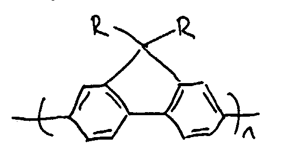
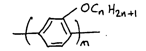
- Materials suitable for the third organic material include polyphenylene derivatives, polyfluorene derivatives, a material such as poly(1,8-octanedioxy-2,6-dimethoxy-1,4-phenylene-1,2-ethenylene-1,4-phenylene-1,2-ethenylene-3,5-dimethoxy-1,4-phenylene), a material such as poly(2,5-diheptyl-1,4-phenylene-alt-2,5-thienylene), thiophene derivatives and PPV-type polymers, especially PPV-type polymers with broken conjugation (e.g. a segmented or meta-linked system).
- Materials suitable for the second organic material include soluble di-alkoxy derivatives of PPV.
- the third organic material is emissive at relatively short visible wavelengths, for example blue.
- the second organic material is emissive at relatively long visible wavelengths, for example red.
- the first organic material is emissive at an intermediate visible wavelength, for example green. Alternatively the first organic material could be non-light-emissive.
- the second component may also comprise a light-emissive material.
- the second component preferably has a wider band gap than the first component.
- the second component preferably comprises a charge transporting and/or charge localising material.
- At least part of one or both of the first and second light-emissive regions preferably lies within 500 ⁇ of one of the charge-carrier injecting layers, preferably the said other of the charge-carrier injecting layers.
- the device may also comprise a third light-emissive region, comprising a fourth organic material, located between the layer of a first organic material and the said one of the charge-carrier injecting layers.
- the fourth organic material preferably has an energy gap between those of the second organic material and the third organic material.
- the third light-emissive region may be integral with the layer of a first organic material, in which case the first organic material and the fourth organic material are preferably the same.
- the device may also comprise a further organic layer, suitably located between the first charge-carrier injecting layer and one or both of the first and second light-emissive regions.
- the further organic layer may comprise a conductive polymer, for example polyaniline, polypyrrole, a derivative of polythiophene or (most preferably) polystyrene sulphonic acid doped polyethylene dioxythiophene ("PEDT-PSS").
- the further organic layer could comprise a molecular or polymeric charge transport material.
- the first emissive region and/or the second emissive region and/or the third emissive region are preferably layers.
- the first region, the second region and the third region are preferably in the same plane in the device structure.
- the first region and/or the second region and/or the third region preferably abut the layer of a first organic material, suitably across the whole of one of their major surfaces.
- the first region and the second region are preferably spaced apart by a zone of the first organic material and/or by the third region.
- the first, second and third regions preferably do not overlap in the device structure.
- the first region and/or the second region and/or the third region are preferably patterned, by any suitable method (e.g. photolithography or ink-jet printing).
- One or both of the charge-injecting layers is preferably patterned to allow the first, second and third regions to be individually addressed for charge-carrier injection.
- the device is preferably a multi-colour display device, preferably a three-colour display device and most preferably a red, green and blue emissive display device.
- Figure 1 shows an electroluminescent device having a glass sheet 1 which carries an anode layer 2 for injecting positive charge-carriers, an organic layer 3, an organic layer 4, an organic layer 5 and a cathode 6.
- the organic layer 3 is formed of PEDT-PSS.
- the organic layer 4 is a blend of PVK blended with a polyfluorene as a blue light-emissive material.
- the organic layer 5 is a layer of PPV (green).
- the anode is formed of ITO and the cathode of an alloy of aluminium and lithium.
- the layers 1 and 2 are provided in the form of a commercially available ITO coated glass substrate, with an ITO resistivity of 15 Ohm/square.
- the ITO is then coated with the layer 3 of PEDT-PSS.
- the PEDT-PSS mixture (see EP 0 686 662 and Bayer AG's Provisional Product Information Sheet for Trial Product Al 4071) is of "EL" grade supplied by Bayer AG. It is filtered and then deposited by spin coating on to the ITO layer at 2000rpm for 60s, yielding a layer roughly 50nm thick.
- the PEDT-PSS layer is then purged in a nitrogen atmosphere for 1 hour, heated for 1 hour at 100°C in a nitrogen atmosphere and then allowed to cool.
- the layer 4 is then deposited.
- the polyfluorene light-emissive component poly(7,7-diheptyl fluorene), in tetrachloroethane solvent, is blended with PVK in tetrachloroethane solvent to give a 2% w/v solution with a 20% w/w/ content of the polyfluorene in PVK.
- This blend is spin-coated over the PEDT-PSS layer at 1100rpm for 50s, yielding a layer approximately 100nm thick.
- the layer 5 is formed by using a roughly 0.5w/v% solution of a precursor to an acetate PPV copolymer spun at 2000rpm for 60s to yield a 15 ⁇ 5nm thickness film. This is purged for 1 hour in a nitrogen atmosphere and then converted for 4 hours at 150°C in a nitrogen atmosphere.
- the precursor polymer and the resulting PPV copolymer are described in more detail in PCT/GB97/02038.
- the cathode 6 is deposited by DC magnetron sputtering from an Al:Li sputter target. During the sputtering process the layer 5 protects the sensitive layer 4 from damage.
- the device is then encapsulated for environmental protection.
- the device can be tested by applying a voltage of 12 to 15V between the anode and the cathode.
- the energy levels of the two components of the organic layer 3 are off-set and the energy-gap of the green PPV is less than that of the blue emitter. Therefore, it would normally be expected that emission of light would principally be from the lower band-gap PPV.
- the voltage is applied across the device, light (of a blue-white colour) is emitted principally from the blue emitter. There is virtually no light emission from the lower band-gap material.
- the through-current at an applied voltage of 12 to 15V is approximately 10 to 15 mA/cm 2 .
- methoxy substituted distyryl benzene with C 8 flexible spacer poly(1,8-octanedioxy-2,6-dimethoxy-1,4-phenylene-1,2-ethenylene-1,4-phenylene-1,2-ethenylene-3,5-dimethoxy-1,4-phenylene) is used.
- the PEDT-PSS layer could be omitted, provided the resulting device had the required stability and current/voltage performance.
- the cathode could be made of other metals or alloys, especially ones having a low work function, for example, calcium.
- Figure 2 shows an embodiment suitable for use as part of a multi-colour display device, in which like components are numbered as for figure 1.
- This embodiment uses the principle described above to provide an improved and simplified structure for a multi-colour device.
- the cathode 6 is patterned to allow the emissive regions 4, 7 and 8 to be individually addressed. In practice it is often necessary to pattern the anode too.
- the device is manufactured as for the one described above, but with the additional red region 7 (which could be of a soluble di-alkoxy PPV derivative) and the green region 8 (which could be of the same material as the layer 5).
- the red region 7 When the red region 7 is addressed the emitted light is red: the red region can emit from lower energy states than the overlying green region.
- the blue region 4 When the blue region 4 is addressed the emitted light is blue, according to the principle described above.
- the green region When the green region is addressed the emitted light is green: it does not matter whether this is emitted from layer 8 or the layer 5, indeed the layers 8 and 5 could be merged and not distinct. Obviously, additional colours and/or colours other than red, green and blue could be provided.
- the present invention may include any feature or combination of features disclosed herein either implicitly or explicitly or any generalisation thereof irrespective of whether it relates to the presently claimed invention.
Landscapes
- Physics & Mathematics (AREA)
- Optics & Photonics (AREA)
- Electroluminescent Light Sources (AREA)
Abstract
Description
- poly(2,5-dihepryl-1,4-phenylene-alt-2,5-thienylene)
in poly(2,5-diheptyl-2',5'-dipentoxy-biphenylene) (see Synthetic Metals 75 (1995) p223)


- a blend of different poly-thiophenes having different energy gaps, including, for
example, poly(3-cyclohexyl-4-methyl-thiophene) (see Nature 372 (1994) p444)

- a blend of soluble polyphenylene derivatives having different energy gaps, such
- s alkyl- and alkoxy-polyphenylenes; - a blend of two or more of the following materials: polyvinylcarbazole ("PVK") (or an equivalent material)






Claims (26)
- An electroluminescent device comprising:a first charge-carrier injecting layer for injecting positive charge-carriers;a second charge-carrier injecting layer for injecting negative charge-carriers;a layer of a first organic material located between the charge-carrier injecting layers; and
located between the layer of a first organic material and one of the charge-carrier injecting layers:a first light-emissive region comprising a light-emissive second organic material having an energy-gap less than that of the first organic material; anda second light-missive region comprising a first component of a light-emissive third organic material having an energy-gap greater than that of the first organic material, and a second component having at least one energy level off-set from that of the first component;
such that when charge-carriers are injected in the first region by the charge-carrier injecting layers light is emitted principally from the second organic material and when charge-carriers are injected in the second region by the charge-carrier injecting layers light is emitted principally from the third organic material. - An electroluminescent device as claimed in claim 1, wherein the first organic material is an at least partially conjugated material.
- An electroluminescent device as claimed in claim 1 or 2, wherein the first organic material is a polymer.
- An electroluminescent device as claimed in any preceding claim, wherein the first organic material is a light-emissive material.
- An electroluminescent device as claimed in any preceding claim, wherein the first organic material comprises poly(p-phenylenevinylene).
- An electroluminescent device as claimed in any preceding claim, wherein the layer of a first organic material is resistant to degradation during a sputter deposition process.
- An electroluminescent device as claimed in any preceding claim, wherein the said one of the charge-injecting layers is the first charge-injecting layer.
- An electroluminescent device as claimed in any preceding claim, wherein the layer of a first organic material abuts the other of the charge-carrier injecting layers.
- An electroluminescent device as claimed in any claim 8, wherein the said other of the charge-carrier injecting layers is a sputter-deposited layer.
- An electroluminescent device as claimed in any preceding claim, wherein the third organic material is an at least partially conjugated material.
- An electroluminescent device as claimed in any preceding claim, wherein the third organic material is a polymer.
- An electroluminescent device as claimed in any preceding claim, wherein the second component comprises a charge transporting and/or charge localising material.
- An electroluminescent device as claimed in any preceding claim, wherein the first organic material is a green-light-emissive material.
- An electroluminescent device as claimed in any preceding claim, wherein the second organic material is a red-light-emissive material.
- An electroluminescent device as claimed in any preceding claim, wherein the third organic material is a blue-light-emissive material.
- An electroluminescent device as claimed in any preceding claim, wherein the second component comprises a light-emissive material.
- An electroluminescent device as claimed in any preceding claim, wherein light emission from the first organic material is essentially suppressed.
- An electroluminescent device as claimed in any preceding claim, wherein the first light-emissive region abuts the layer of a first organic material.
- An electroluminescent device as claimed in any preceding claim, wherein the second light-emissive region abuts the layer of a first organic material.
- An electroluminescent device as claimed in any preceding claim, wherein the second charge-carrier injecting layer is a metal or alloy having a work function less than 3.5eV.
- An electroluminescent device as claimed in any preceding claim, wherein the thickness of the layer of a first organic material is less than 500Å.
- An electroluminescent device as claimed in claim 21, wherein the second light-emissive region is located within 500Å from the said one of the charge-injecting layers.
- An electroluminescent device as claimed in any preceding claim, wherein a further layer comprising a conductive polymer is located between the other of the charge-carrier injecting layers and the first light emissive region.
- A method for producing an electroluminescent device, comprising the steps of:depositing a first charge-carrier injecting layer for injecting positive charge-carriers;depositing a first light-emissive region comprising a light-emissive first organic material; anddepositing a second light-missive region comprising a first component of a light-missive second organic material, and a second component having at least one energy level off-set from that of the first component;depositing a layer of a third organic material resistant to degradation during a sputter deposition process and having an energy gap greater than that of the first organic material and less than that of the second organic material; anddepositing a second charge-carrier injecting layer for injecting negative charge-carriers;
to provide a device such that when charge-carriers are injected in the first region by the charge-carrier injecting layers light is emitted principally from the first organic material and when charge-carriers are injected in the second region by the charge-carrier injecting layers light is emitted principally from the second organic material. - A method as claimed in claim 24, wherein the second charge-carrier injecting layer is deposited by sputtering.
- A method as claimed in claim 25, wherein the second charge-carrier injecting layer is deposited by DC magnetron sputtering.
Applications Claiming Priority (2)
| Application Number | Priority Date | Filing Date | Title |
|---|---|---|---|
| GB9724682 | 1997-11-21 | ||
| GBGB9724682.1A GB9724682D0 (en) | 1997-11-21 | 1997-11-21 | Electroluminescent device |
Publications (3)
| Publication Number | Publication Date |
|---|---|
| EP0921578A2 true EP0921578A2 (en) | 1999-06-09 |
| EP0921578A3 EP0921578A3 (en) | 2001-10-17 |
| EP0921578B1 EP0921578B1 (en) | 2015-07-01 |
Family
ID=10822470
Family Applications (1)
| Application Number | Title | Priority Date | Filing Date |
|---|---|---|---|
| EP98309500.1A Expired - Lifetime EP0921578B1 (en) | 1997-11-21 | 1998-11-19 | Electroluminescent device |
Country Status (3)
| Country | Link |
|---|---|
| US (1) | US6384528B1 (en) |
| EP (1) | EP0921578B1 (en) |
| GB (1) | GB9724682D0 (en) |
Cited By (1)
| Publication number | Priority date | Publication date | Assignee | Title |
|---|---|---|---|---|
| US7829203B2 (en) | 2002-03-09 | 2010-11-09 | Cdt Oxford Limited | Polymerisable compositions and organic light-emitting devices containing them |
Families Citing this family (34)
| Publication number | Priority date | Publication date | Assignee | Title |
|---|---|---|---|---|
| US8853696B1 (en) | 1999-06-04 | 2014-10-07 | Semiconductor Energy Laboratory Co., Ltd. | Electro-optical device and electronic device |
| TW522453B (en) * | 1999-09-17 | 2003-03-01 | Semiconductor Energy Lab | Display device |
| US20020036291A1 (en) | 2000-06-20 | 2002-03-28 | Parker Ian D. | Multilayer structures as stable hole-injecting electrodes for use in high efficiency organic electronic devices |
| KR100478521B1 (en) * | 2001-10-29 | 2005-03-28 | 삼성에스디아이 주식회사 | Emitting composition mixture polymer and electroluminescence device using the same |
| KR100478522B1 (en) * | 2001-11-28 | 2005-03-28 | 삼성에스디아이 주식회사 | Polymeric electroluminescent device comprising organic compound layer and method thereof |
| US7453202B2 (en) | 2001-11-28 | 2008-11-18 | Samsung Sdi Co., Ltd. | Organic EL display device having organic soluble derivative layer |
| US7275972B2 (en) * | 2003-08-22 | 2007-10-02 | 3M Innovative Properties Company | Method of making an electroluminescent device having a patterned emitter layer and non-patterned emitter layer |
| US7011529B2 (en) * | 2004-03-01 | 2006-03-14 | Anritsu Company | Hermetic glass bead assembly having high frequency compensation |
| US20050255253A1 (en) * | 2004-05-13 | 2005-11-17 | White John M | Apparatus and methods for curing ink on a substrate using an electron beam |
| US20060109296A1 (en) * | 2004-11-04 | 2006-05-25 | Bassam Shamoun | Methods and apparatus for inkjet printing color filters for displays |
| US7413272B2 (en) * | 2004-11-04 | 2008-08-19 | Applied Materials, Inc. | Methods and apparatus for precision control of print head assemblies |
| US7556334B2 (en) * | 2004-11-04 | 2009-07-07 | Applied Materials, Inc. | Methods and apparatus for aligning print heads |
| US20060093751A1 (en) * | 2004-11-04 | 2006-05-04 | Applied Materials, Inc. | System and methods for inkjet printing for flat panel displays |
| US20060092218A1 (en) * | 2004-11-04 | 2006-05-04 | Applied Materials, Inc. | Methods and apparatus for inkjet printing |
| US20070042113A1 (en) * | 2004-11-04 | 2007-02-22 | Applied Materials, Inc. | Methods and apparatus for inkjet printing color filters for displays using pattern data |
| US20060185587A1 (en) * | 2005-02-18 | 2006-08-24 | Applied Materials, Inc. | Methods and apparatus for reducing ink conglomerates during inkjet printing for flat panel display manufacturing |
| TWI318685B (en) * | 2005-07-28 | 2009-12-21 | Applied Materials Inc | Methods and apparatus for concurrent inkjet printing and defect inspection |
| US20070070132A1 (en) * | 2005-09-27 | 2007-03-29 | Fan-Cheung Sze | Inkjet delivery module |
| US20070068560A1 (en) * | 2005-09-29 | 2007-03-29 | Quanyuan Shang | Methods and apparatus for inkjet print head cleaning |
| US20070076040A1 (en) * | 2005-09-29 | 2007-04-05 | Applied Materials, Inc. | Methods and apparatus for inkjet nozzle calibration |
| US7611217B2 (en) * | 2005-09-29 | 2009-11-03 | Applied Materials, Inc. | Methods and systems for inkjet drop positioning |
| US20070070109A1 (en) * | 2005-09-29 | 2007-03-29 | White John M | Methods and systems for calibration of inkjet drop positioning |
| US20080018677A1 (en) * | 2005-09-29 | 2008-01-24 | White John M | Methods and apparatus for inkjet print head cleaning using an inflatable bladder |
| US7923057B2 (en) * | 2006-02-07 | 2011-04-12 | Applied Materials, Inc. | Methods and apparatus for reducing irregularities in color filters |
| US20070263026A1 (en) * | 2006-04-29 | 2007-11-15 | Quanyuan Shang | Methods and apparatus for maintaining inkjet print heads using parking structures |
| US20070252863A1 (en) * | 2006-04-29 | 2007-11-01 | Lizhong Sun | Methods and apparatus for maintaining inkjet print heads using parking structures with spray mechanisms |
| US20070256709A1 (en) * | 2006-04-29 | 2007-11-08 | Quanyuan Shang | Methods and apparatus for operating an inkjet printing system |
| US20080024532A1 (en) * | 2006-07-26 | 2008-01-31 | Si-Kyoung Kim | Methods and apparatus for inkjet printing system maintenance |
| WO2008013902A2 (en) * | 2006-07-28 | 2008-01-31 | Applied Materials, Inc. | Methods and apparatus for improved manufacturing of color filters |
| US20080204501A1 (en) * | 2006-12-01 | 2008-08-28 | Shinichi Kurita | Inkjet print head pressure regulator |
| US7857413B2 (en) | 2007-03-01 | 2010-12-28 | Applied Materials, Inc. | Systems and methods for controlling and testing jetting stability in inkjet print heads |
| US7637587B2 (en) * | 2007-08-29 | 2009-12-29 | Applied Materials, Inc. | System and method for reliability testing and troubleshooting inkjet printers |
| WO2009116547A1 (en) | 2008-03-18 | 2009-09-24 | Semiconductor Energy Laboratory Co., Ltd. | Light-emitting element, light-emitting device and electronic device |
| CN101978784B (en) | 2008-03-18 | 2012-12-05 | 株式会社半导体能源研究所 | Light emitting element, light emitting device and electronic device |
Family Cites Families (16)
| Publication number | Priority date | Publication date | Assignee | Title |
|---|---|---|---|---|
| US5104683A (en) * | 1987-12-31 | 1992-04-14 | The United States Of America As Represented By The Administrator Of The National Aeronautics And Space Administration | Single layer multi-color luminescent display and method of making |
| EP0390551B1 (en) | 1989-03-31 | 1996-07-10 | Kabushiki Kaisha Toshiba | Organic electroluminescent device |
| GB8909011D0 (en) | 1989-04-20 | 1989-06-07 | Friend Richard H | Electroluminescent devices |
| US5294870A (en) * | 1991-12-30 | 1994-03-15 | Eastman Kodak Company | Organic electroluminescent multicolor image display device |
| EP0553950A3 (en) | 1992-01-07 | 1994-11-23 | Toshiba Kk | Organic electroluminescent device |
| WO1993021744A1 (en) * | 1992-04-16 | 1993-10-28 | Kabushiki Kaisha Komatsu Seisakusho | Thin-film el element |
| GB9215929D0 (en) | 1992-07-27 | 1992-09-09 | Cambridge Display Tech Ltd | Electroluminescent devices |
| GB9317932D0 (en) | 1993-08-26 | 1993-10-13 | Cambridge Display Tech Ltd | Electroluminescent devices |
| EP0686662B2 (en) | 1994-05-06 | 2006-05-24 | Bayer Ag | Conductive coatings |
| JP2848277B2 (en) * | 1994-08-02 | 1999-01-20 | 株式会社デンソー | EL element manufacturing method |
| US5707745A (en) | 1994-12-13 | 1998-01-13 | The Trustees Of Princeton University | Multicolor organic light emitting devices |
| US5693428A (en) * | 1995-02-06 | 1997-12-02 | Sanyo Electric Co., Ltd. | Organic electroluminescent device |
| JP3143350B2 (en) * | 1995-02-06 | 2001-03-07 | 三洋電機株式会社 | Organic electroluminescence device |
| KR0170490B1 (en) * | 1995-12-22 | 1999-05-01 | 양승택 | Color display element using electroluminescence and its manufacturing method |
| US5773130A (en) * | 1996-06-06 | 1998-06-30 | Motorola, Inc. | Multi-color organic electroluminescent device |
| US6423428B1 (en) | 1996-07-29 | 2002-07-23 | Cambridge Display Technology Limited | Conjugated copolymers for use in luminescent devices |
-
1997
- 1997-11-21 GB GBGB9724682.1A patent/GB9724682D0/en not_active Ceased
-
1998
- 1998-11-19 EP EP98309500.1A patent/EP0921578B1/en not_active Expired - Lifetime
- 1998-11-20 US US09/196,983 patent/US6384528B1/en not_active Expired - Lifetime
Cited By (2)
| Publication number | Priority date | Publication date | Assignee | Title |
|---|---|---|---|---|
| US7829203B2 (en) | 2002-03-09 | 2010-11-09 | Cdt Oxford Limited | Polymerisable compositions and organic light-emitting devices containing them |
| US8883321B2 (en) | 2002-03-09 | 2014-11-11 | Cdt Oxford Limited | Polymerizable compositions and organic light-emitting devices containing them |
Also Published As
| Publication number | Publication date |
|---|---|
| EP0921578B1 (en) | 2015-07-01 |
| EP0921578A3 (en) | 2001-10-17 |
| GB9724682D0 (en) | 1998-01-21 |
| US6384528B1 (en) | 2002-05-07 |
Similar Documents
| Publication | Publication Date | Title |
|---|---|---|
| EP0921578B1 (en) | Electroluminescent device | |
| US6551727B2 (en) | Electroluminescent device | |
| EP1983805B1 (en) | Organic electroluminescent element | |
| US5798170A (en) | Long operating life for polymer light-emitting diodes | |
| Yang et al. | Electron injection polymer for polymer light‐emitting diodes | |
| US6784016B2 (en) | Organic light-emitting devices with blocking and transport layers | |
| Wang et al. | Multicolor multilayer light-emitting devices based on pyridine-containing conjugated polymers and para-sexiphenyl oligomer | |
| Chen et al. | 1 micron wavelength photo-and electroluminescence from a conjugated polymer | |
| US20080003456A1 (en) | Methods for producing electroluminescent devices by screen printing | |
| US20070182316A1 (en) | OLED with Area Defined Multicolor Emission Within a Single Lighting Element | |
| JP4210093B2 (en) | Organic electroluminescent image display device | |
| US7576356B2 (en) | Solution processed crosslinkable hole injection and hole transport polymers for OLEDs | |
| KR20110052599A (en) | Organic electroluminescent device and manufacturing method thereof | |
| US6809472B1 (en) | Light-emitting devices | |
| US7626332B2 (en) | Luminance uniformity enhancement methods for an OLED light source | |
| US6897491B2 (en) | Display with dummy edge electrode | |
| US20090121616A1 (en) | Light-emitting diode with luminescent charge transport layer | |
| TW550971B (en) | Organic light-emitting devices with blocking and transport layers | |
| Onoda et al. | Organic Display Devices Using Poly (Arylene Vinylene) Conducting Polymers | |
| Liu et al. | Dual-color polymer light-emitting diodes based on hybrid films of soluble poly (p-phenylenevinylene) derivatives | |
| HK1051439A (en) | Electroluminescent device |
Legal Events
| Date | Code | Title | Description |
|---|---|---|---|
| PUAI | Public reference made under article 153(3) epc to a published international application that has entered the european phase |
Free format text: ORIGINAL CODE: 0009012 |
|
| AK | Designated contracting states |
Kind code of ref document: A2 Designated state(s): AT BE CH CY DE DK ES FI FR GB GR IE IT LI LU MC NL PT SE Kind code of ref document: A2 Designated state(s): DE FR GB |
|
| AX | Request for extension of the european patent |
Free format text: AL;LT;LV;MK;RO;SI |
|
| PUAL | Search report despatched |
Free format text: ORIGINAL CODE: 0009013 |
|
| AK | Designated contracting states |
Kind code of ref document: A3 Designated state(s): AT BE CH CY DE DK ES FI FR GB GR IE IT LI LU MC NL PT SE |
|
| AX | Request for extension of the european patent |
Free format text: AL;LT;LV;MK;RO;SI |
|
| 17P | Request for examination filed |
Effective date: 20020412 |
|
| AKX | Designation fees paid |
Free format text: DE FR GB |
|
| 111Z | Information provided on other rights and legal means of execution |
Free format text: DEFRGB Effective date: 20040930 |
|
| 17Q | First examination report despatched |
Effective date: 20071221 |
|
| RAP1 | Party data changed (applicant data changed or rights of an application transferred) |
Owner name: CAMBRIDGE DISPLAY TECHNOLOGY LIMITED |
|
| REG | Reference to a national code |
Ref country code: DE Ref legal event code: R079 Ref document number: 69843411 Country of ref document: DE Free format text: PREVIOUS MAIN CLASS: H01L0051200000 Ipc: H01L0051500000 |
|
| GRAP | Despatch of communication of intention to grant a patent |
Free format text: ORIGINAL CODE: EPIDOSNIGR1 |
|
| INTG | Intention to grant announced |
Effective date: 20150130 |
|
| RIC1 | Information provided on ipc code assigned before grant |
Ipc: H01L 27/32 20060101ALI20150116BHEP Ipc: H01L 51/50 20060101AFI20150116BHEP |
|
| GRAS | Grant fee paid |
Free format text: ORIGINAL CODE: EPIDOSNIGR3 |
|
| GRAA | (expected) grant |
Free format text: ORIGINAL CODE: 0009210 |
|
| AK | Designated contracting states |
Kind code of ref document: B1 Designated state(s): DE FR GB |
|
| REG | Reference to a national code |
Ref country code: GB Ref legal event code: FG4D |
|
| REG | Reference to a national code |
Ref country code: DE Ref legal event code: R096 Ref document number: 69843411 Country of ref document: DE |
|
| REG | Reference to a national code |
Ref country code: DE Ref legal event code: R097 Ref document number: 69843411 Country of ref document: DE |
|
| PLBE | No opposition filed within time limit |
Free format text: ORIGINAL CODE: 0009261 |
|
| STAA | Information on the status of an ep patent application or granted ep patent |
Free format text: STATUS: NO OPPOSITION FILED WITHIN TIME LIMIT |
|
| 26N | No opposition filed |
Effective date: 20160404 |
|
| REG | Reference to a national code |
Ref country code: FR Ref legal event code: ST Effective date: 20160729 |
|
| PG25 | Lapsed in a contracting state [announced via postgrant information from national office to epo] |
Ref country code: FR Free format text: LAPSE BECAUSE OF NON-PAYMENT OF DUE FEES Effective date: 20151130 |
|
| PGFP | Annual fee paid to national office [announced via postgrant information from national office to epo] |
Ref country code: DE Payment date: 20171130 Year of fee payment: 20 |
|
| PGFP | Annual fee paid to national office [announced via postgrant information from national office to epo] |
Ref country code: GB Payment date: 20171026 Year of fee payment: 20 |
|
| REG | Reference to a national code |
Ref country code: DE Ref legal event code: R071 Ref document number: 69843411 Country of ref document: DE |
|
| REG | Reference to a national code |
Ref country code: GB Ref legal event code: PE20 Expiry date: 20181118 |
|
| PG25 | Lapsed in a contracting state [announced via postgrant information from national office to epo] |
Ref country code: GB Free format text: LAPSE BECAUSE OF EXPIRATION OF PROTECTION Effective date: 20181118 |