EP0917285B1 - Low-voltage amplifiers - Google Patents
Low-voltage amplifiers Download PDFInfo
- Publication number
- EP0917285B1 EP0917285B1 EP98308484A EP98308484A EP0917285B1 EP 0917285 B1 EP0917285 B1 EP 0917285B1 EP 98308484 A EP98308484 A EP 98308484A EP 98308484 A EP98308484 A EP 98308484A EP 0917285 B1 EP0917285 B1 EP 0917285B1
- Authority
- EP
- European Patent Office
- Prior art keywords
- amplifier
- transistors
- common
- emitter
- transistor
- Prior art date
- Legal status (The legal status is an assumption and is not a legal conclusion. Google has not performed a legal analysis and makes no representation as to the accuracy of the status listed.)
- Expired - Lifetime
Links
Images

Classifications
-
- H—ELECTRICITY
- H03—ELECTRONIC CIRCUITRY
- H03F—AMPLIFIERS
- H03F1/00—Details of amplifiers with only discharge tubes, only semiconductor devices or only unspecified devices as amplifying elements
- H03F1/02—Modifications of amplifiers to raise the efficiency, e.g. gliding Class A stages, use of an auxiliary oscillation
-
- H—ELECTRICITY
- H03—ELECTRONIC CIRCUITRY
- H03D—DEMODULATION OR TRANSFERENCE OF MODULATION FROM ONE CARRIER TO ANOTHER
- H03D7/00—Transference of modulation from one carrier to another, e.g. frequency-changing
- H03D7/14—Balanced arrangements
-
- H—ELECTRICITY
- H03—ELECTRONIC CIRCUITRY
- H03D—DEMODULATION OR TRANSFERENCE OF MODULATION FROM ONE CARRIER TO ANOTHER
- H03D7/00—Transference of modulation from one carrier to another, e.g. frequency-changing
- H03D7/14—Balanced arrangements
- H03D7/1425—Balanced arrangements with transistors
- H03D7/1433—Balanced arrangements with transistors using bipolar transistors
-
- H—ELECTRICITY
- H03—ELECTRONIC CIRCUITRY
- H03D—DEMODULATION OR TRANSFERENCE OF MODULATION FROM ONE CARRIER TO ANOTHER
- H03D7/00—Transference of modulation from one carrier to another, e.g. frequency-changing
- H03D7/14—Balanced arrangements
- H03D7/1425—Balanced arrangements with transistors
- H03D7/1491—Arrangements to linearise a transconductance stage of a mixer arrangement
-
- H—ELECTRICITY
- H03—ELECTRONIC CIRCUITRY
- H03F—AMPLIFIERS
- H03F3/00—Amplifiers with only discharge tubes or only semiconductor devices as amplifying elements
- H03F3/26—Push-pull amplifiers; Phase-splitters therefor
-
- H—ELECTRICITY
- H03—ELECTRONIC CIRCUITRY
- H03D—DEMODULATION OR TRANSFERENCE OF MODULATION FROM ONE CARRIER TO ANOTHER
- H03D2200/00—Indexing scheme relating to details of demodulation or transference of modulation from one carrier to another covered by H03D
- H03D2200/0001—Circuit elements of demodulators
- H03D2200/0033—Current mirrors
-
- H—ELECTRICITY
- H03—ELECTRONIC CIRCUITRY
- H03D—DEMODULATION OR TRANSFERENCE OF MODULATION FROM ONE CARRIER TO ANOTHER
- H03D2200/00—Indexing scheme relating to details of demodulation or transference of modulation from one carrier to another covered by H03D
- H03D2200/0041—Functional aspects of demodulators
- H03D2200/0043—Bias and operating point
-
- H—ELECTRICITY
- H03—ELECTRONIC CIRCUITRY
- H03F—AMPLIFIERS
- H03F2200/00—Indexing scheme relating to amplifiers
- H03F2200/513—Indexing scheme relating to amplifiers the amplifier being made for low supply voltages
Definitions
- the present invention relates to low-voltage amplifiers, and in particular although not exclusively to low-voltage amplifiers for use in radiotelephones.
- the lower supply voltage can make it difficult to design large-signal handling circuits around standard integrated circuit mixer configurations, such as Gilbert cells, which usually require a number of active devices to be stacked between the supply rails in order to be current efficient.
- active devices may include, for example, the transistors of an input amplifier by means of which unbalanced or single-ended radio frequency received signals are amplified and phase-split to provide the balanced or differential current signals required to drive the transistors of a mixer cell.
- EP-A-0584870 shows at Figure 2 thereof a transconductance amplifier comprising a common base transistor and a common emitter transistor arranged to receive a single-ended input signal and to provide differential current signals at their collector electrodes.
- this amplifier is not a low-voltage amplifier, and the present invention seeks to provide a low-voltage amplifier having improved or comparable transfer characteristics yet operable at lower voltages than this prior art amplifier.
- US-A-5365192 describes a single-ended or differential-input radio frequency amplifier integrated circuit which includes a first transistor in a common-emitter configuration coupled to a second transistor in a common-base configuration.
- a low voltage amplifier for providing differential current outputs from a single-ended input comprising first and second transistors connected to receive signals from said input respectively in common-base and common-emitter configuration and means to forward bias the base-emitter junctions of said transistors, the differential outputs being derived from the collector electrodes of said first and second transistors, characterised by the biasing means being arranged such that the emitter electrodes of the first and second transistors may be operated to be at a potential which is substantially that of a common supply line (9) of the amplifier.
- the first transistor is connected to receive signals from said input in common-base configuration by an impedance
- the second transistor is connected to receive signals from said input in a common-emitter configuration by a capacitor.
- the capacitor acts as a d.c. block which therefore allows the base voltage of the common-base connected transistor to be independent of the base voltage of the common-emitter connected transistor. This allows more voltage headroom above the amplifier and can provide linearity and gain prior art common-base/common-emitter transistor amplifiers.
- the means to forward bias the base-emitter junctions of the first and second transistors may comprise a third transistor connected in a current-mirror configuration.
- a low voltage amplifier for selectively providing differential current outputs from one or more of at least two amplifier stages in response to signals applied to a single-ended input (8) common to the amplifier stages, characterised in that each amplifier stage comprises a low voltage amplifier as defined in claim 1, wherein the emitter electrodes of at least two of said first transistors being connected by a common first inductor to input and the emitter electrodes of at least two of said second transistors being connected by a common second inductor to a negative voltage supply line, the differential outputs of an amplifier stage being derived from the collector electrodes of the first and second transistors of that stage.
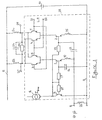
- a low-voltage amplifier comprising first, second and third transistors 1, 2 and 3, forms the input stage for a mixer stage comprising transistors 4, 5, 6 and 7.
- a radio frequency input signal is arranged to be applied between an input terminal 8 and a common negative supply line or rail 9.
- a battery 10 providing, for example, 2.7 volts, may be connected between the line 9 and a positive supply line 11.
- the input terminal 8 is connected by way of a first inductor 12 to the emitter electrode of the first transistor 1 and by way of a first capacitor 13 to the base electrode of the second transistor 2, radio-frequency return paths to the line 9 being completed by way of a second capacitor 14 from the base electrode of the first transistor 1 and by way of a second inductor 15 from the emitter electrode of the second transistor 2.
- Direct-current bias for the first and second transistors 1 and 2 is provided by biasing means comprising a current-mirror arrangement formed by a current source 16 and a third transistor 3, with first, second and third biasing resistors 17, 18 and 19 connecting the collector circuit of the third transistor 3 to the base electrodes respectively of the first and second transistors 1 and 2 and the third transistor 3.
- the values of these resistors may be chosen to set the required values of current flow through the first and second transistors 1 and 2, compensating for their finite current gains.
- the second resistor 18 also provides a measure of radio frequency isolation of the bias arrangement from the radio frequency signals at the base electrode of the second transistor 2, while the first capacitor 13 provides a DC block to the bias at the base electrode of the second transistor 2.
- a direct current path to the line 9 for the emitter current of the first transistor 1 is provided by way of an inductor or rf choke 20 between the input terminal 8 and the line 9, the reactance of this choke 20 being accounted for in the design of the matching network normally provided at the input terminal 8.
- the first transistor 1 is connected in common-base configuration while the second transistor 2 is connected in common-emitter configuration, so that in response to radio frequency signals at the input terminal 8, differential current signals are provided from the collector electrodes of the first and second transistors 1 and 2 to drive the mixer stage transistors 4 and 5 and 6 and 7 respectively.
- differential current signals are mixed in operation with local oscillator signals applied at terminals 21 and 22, and intermediate frequency output signals from the cross-coupled collector electrodes of the mixer transistors 4 to 7 are applied to a load circuit comprising load inductors 23 and 24 and a filter circuit comprising a resistor 25 and a capacitor 26.
- Differential output voltage signals at intermediate frequency may be taken from first and second output terminals 27 and 28.
- the first and second inductors 12 and 15 provide a measure of inductive degeneration, although this is not essential to the operation of the amplifier.
- the inductors 12, 15 and 20 may be considered as very close to DC short circuit.
- the biasing means 3, 16, 14, 15, 12 enables the first and second transistors 1 and 2 to have their emitter electrodes very close to the potential of the line 9, thus maximising the proportion of the supply voltage which remains available to the rest of the circuit, that is, the mixer stage and the load circuit, where the largest voltage swings are to be expected.
- the amplifier and mixer described above may be formed on an integrated circuit chip, indicated by the dashed outline 29, the choke 20 and the components 23 to 26 of the load circuit being provided externally, as shown, or on-chip.
- the inductors 12 and 15 can each take up a large area on the integrated circuit on which they are formed. The inventors have found that these inductors can be used also by one or more further amplifier circuits formed on the same integrated circuit.
- Figure 2 shows a low-voltage amplifier having two amplifying circuits.
- a first amplifier stage comprises the amplifier of Figure 1, from which reference numerals have been re-used for like elements.
- the first amplifier stage is connected to a mixer core formed from transistors 4 to 7, as in Figure 1.
- a second amplifier stage is formed from fourth, fifth and sixth transistors 30, 31 and 32, each biased by their respective one of biasing resistors 34, 33 and 35.
- the base of the fourth transistor 30 is connected to the negative supply line 9 by a third capacitor 36 and the base of the fifth transistor 31 is connected to the input terminal 8 by a fourth capacitor 37.
- the emitter of the fourth transistor 30 is connected to the input terminal 8 by the first inductor 12, which it thereby shares with the first transistor 1.
- the fifth transistor 31 similarly shares the second inductor 15 with the second transistor 2.
- the collector electrodes of the fourth and fifth transistors 30 and 31 form respective ones of differential current inputs to a second mixer core formed by transistors 38, 39, 40 and 41.
- the second mixer core is arranged to receive local oscillator signals on local oscillator input terminals 42 and 43.
- a load circuit formed by load inductors 44 and 45 and a filter circuit formed by a capacitor 46 and a resistor 47 are connected between the output of the second mixer core and the positive supply line 11 and third and fourth output terminals 48 and 49 are provided in much the same way as the load and filter circuit arrangement of the first mixer core formed by the components 23 to 28.
- the first amplifier stage is selected to handle signals applied to the input terminal 8 by switching on the current source 16 with the use of external control circuitry (not shown).
- the second amplifier stage can similarly be selected for handling the signal applied to the input terminal 8 by selection of its current source 50, by the same or similar external control circuitry (not shown). Whichever of the first and second amplifier stages is selected, its performance will not be compromised by the connection of the first and second transistors 1 and 2 or the fourth and fifth transistors 30 and 31 as the case may be because of the high emitter impedance of these transistors.
- Figure 2 low-voltage amplifier arrangement will be of particular use in applications where the use of a variable frequency local oscillator is impractical, expensive or otherwise undesirable.
- the Figure 2 arrangement can allow two, different, fixed frequency local oscillator signals to be mixed with a single input RF signal using the circuitry formed on single integrated circuit. It is possible even to select both the first and the second amplifier stages at the same time, providing output signals on the terminals 27 and 28 and the terminals 48 and 49 simultaneously. Such output signals would of course be derived from the same input signal, but would be dependent on the local oscillator signals applied to their respective local oscillator input terminals 21, 22 and 42, 43.
- the first amplifier stage With the Figure 2 arrangement, it is possible to provide easily the first amplifier stage with a different gain to that of the second amplifier stage. Although this could be achieved by the fabrication of the fourth and fifth transistors 30 and 31 with different properties to those of the first and second transistors 1 and 2, the first and second inductors 12 and 15 could be connected in the following way to achieve the same effect. If, for example, the first and second transistors 1 and 2 are connected to the outermost end of a respective five turn inductor 12 and 15 and the input terminal 8 and the negative supply line 9 are connected respectively to the innermost ends of the inductors 12 and 15, the second amplifier stage could be provided with a higher gain by connecting the fourth and fifth transistors 30 and 31 to the fourth or to the third turn of the inductors 12 and 15.
- each further amplifier stage would require its own voltage biasing means, preferably a current source connected in a current mirror configuration as in the first and second amplifier stages shown in Figure 2.
- These further amplifier stages could share the inductors 12 and 15, or could involve separate inductors.
Description
- The present invention relates to low-voltage amplifiers, and in particular although not exclusively to low-voltage amplifiers for use in radiotelephones.
- The demands for large-signal handling capability in radiotelephones and in particular cellular phone circuits such as low-noise amplifiers and mixers are increasing, while the supply voltages on which they are required to operate are decreasing. For example, a few years ago battery voltages of 4.8 volts were common, whereas today cellular phone circuits may be required to operate from a 2.7 volt supply.
- The lower supply voltage can make it difficult to design large-signal handling circuits around standard integrated circuit mixer configurations, such as Gilbert cells, which usually require a number of active devices to be stacked between the supply rails in order to be current efficient. These active devices may include, for example, the transistors of an input amplifier by means of which unbalanced or single-ended radio frequency received signals are amplified and phase-split to provide the balanced or differential current signals required to drive the transistors of a mixer cell.
- EP-A-0584870 shows at Figure 2 thereof a transconductance amplifier comprising a common base transistor and a common emitter transistor arranged to receive a single-ended input signal and to provide differential current signals at their collector electrodes. However, this amplifier is not a low-voltage amplifier, and the present invention seeks to provide a low-voltage amplifier having improved or comparable transfer characteristics yet operable at lower voltages than this prior art amplifier.
- US-A-5365192 describes a single-ended or differential-input radio frequency amplifier integrated circuit which includes a first transistor in a common-emitter configuration coupled to a second transistor in a common-base configuration.
- According to a first aspect of the present invention, there is provided a low voltage amplifier for providing differential current outputs from a single-ended input comprising first and second transistors connected to receive signals from said input respectively in common-base and common-emitter configuration and means to forward bias the base-emitter junctions of said transistors, the differential outputs being derived from the collector electrodes of said first and second transistors, characterised by the biasing means being arranged such that the emitter electrodes of the first and second transistors may be operated to be at a potential which is substantially that of a common supply line (9) of the amplifier.
- According to a second aspect of the present invention, the first transistor is connected to receive signals from said input in common-base configuration by an impedance, wherein the second transistor is connected to receive signals from said input in a common-emitter configuration by a capacitor.
- The capacitor acts as a d.c. block which therefore allows the base voltage of the common-base connected transistor to be independent of the base voltage of the common-emitter connected transistor. This allows more voltage headroom above the amplifier and can provide linearity and gain prior art common-base/common-emitter transistor amplifiers.
- The means to forward bias the base-emitter junctions of the first and second transistors may comprise a third transistor connected in a current-mirror configuration.
- According to a third aspect of the present invention, there is provided a low voltage amplifier for selectively providing differential current outputs from one or more of at least two amplifier stages in response to signals applied to a single-ended input (8) common to the amplifier stages, characterised in that each amplifier stage comprises a low voltage amplifier as defined in
claim 1, wherein the emitter electrodes of at least two of said first transistors being connected by a common first inductor to input and the emitter electrodes of at least two of said second transistors being connected by a common second inductor to a negative voltage supply line, the differential outputs of an amplifier stage being derived from the collector electrodes of the first and second transistors of that stage. - Embodiments of the present invention will now be described by way of example only with reference to the accompanying drawings of:
- Figure 1 shows a low-voltage amplifier in accordance with the first and second aspects of the present invention; and
- Figure 2 shows a low-voltage amplifier in accordance with the first, second and third aspects of the present invention.
-
- Referring to Figure 1, a low-voltage amplifier, comprising first, second and
third transistors stage comprising transistors input terminal 8 and a common negative supply line orrail 9. Abattery 10 providing, for example, 2.7 volts, may be connected between theline 9 and apositive supply line 11. - The
input terminal 8 is connected by way of afirst inductor 12 to the emitter electrode of thefirst transistor 1 and by way of afirst capacitor 13 to the base electrode of thesecond transistor 2, radio-frequency return paths to theline 9 being completed by way of asecond capacitor 14 from the base electrode of thefirst transistor 1 and by way of asecond inductor 15 from the emitter electrode of thesecond transistor 2. - Direct-current bias for the first and
second transistors current source 16 and athird transistor 3, with first, second andthird biasing resistors third transistor 3 to the base electrodes respectively of the first andsecond transistors third transistor 3. The values of these resistors may be chosen to set the required values of current flow through the first andsecond transistors second resistor 18 also provides a measure of radio frequency isolation of the bias arrangement from the radio frequency signals at the base electrode of thesecond transistor 2, while thefirst capacitor 13 provides a DC block to the bias at the base electrode of thesecond transistor 2. A direct current path to theline 9 for the emitter current of thefirst transistor 1 is provided by way of an inductor or rf choke 20 between theinput terminal 8 and theline 9, the reactance of this choke 20 being accounted for in the design of the matching network normally provided at theinput terminal 8. - It will be seen that for radio frequency signals the
first transistor 1 is connected in common-base configuration while thesecond transistor 2 is connected in common-emitter configuration, so that in response to radio frequency signals at theinput terminal 8, differential current signals are provided from the collector electrodes of the first andsecond transistors mixer stage transistors terminals mixer transistors 4 to 7 are applied to a load circuit comprisingload inductors resistor 25 and acapacitor 26. Differential output voltage signals at intermediate frequency may be taken from first andsecond output terminals - The first and
second inductors inductors second transistors line 9, thus maximising the proportion of the supply voltage which remains available to the rest of the circuit, that is, the mixer stage and the load circuit, where the largest voltage swings are to be expected. - The amplifier and mixer described above may be formed on an integrated circuit chip, indicated by the
dashed outline 29, the choke 20 and thecomponents 23 to 26 of the load circuit being provided externally, as shown, or on-chip. - Although only a preferred feature of the present invention, the
inductors - Referring to Figure 2, a first amplifier stage comprises the amplifier of Figure 1, from which reference numerals have been re-used for like elements. The first amplifier stage is connected to a mixer core formed from
transistors 4 to 7, as in Figure 1. A second amplifier stage is formed from fourth, fifth andsixth transistors biasing resistors fourth transistor 30 is connected to thenegative supply line 9 by a third capacitor 36 and the base of thefifth transistor 31 is connected to theinput terminal 8 by afourth capacitor 37. The emitter of thefourth transistor 30 is connected to theinput terminal 8 by thefirst inductor 12, which it thereby shares with thefirst transistor 1. Thefifth transistor 31 similarly shares thesecond inductor 15 with thesecond transistor 2. - The collector electrodes of the fourth and
fifth transistors transistors oscillator input terminals 42 and 43. A load circuit formed byload inductors resistor 47 are connected between the output of the second mixer core and thepositive supply line 11 and third andfourth output terminals 48 and 49 are provided in much the same way as the load and filter circuit arrangement of the first mixer core formed by thecomponents 23 to 28. - The first amplifier stage is selected to handle signals applied to the
input terminal 8 by switching on thecurrent source 16 with the use of external control circuitry (not shown). The second amplifier stage can similarly be selected for handling the signal applied to theinput terminal 8 by selection of its current source 50, by the same or similar external control circuitry (not shown). Whichever of the first and second amplifier stages is selected, its performance will not be compromised by the connection of the first andsecond transistors fifth transistors - It is contemplated that the Figure 2 low-voltage amplifier arrangement will be of particular use in applications where the use of a variable frequency local oscillator is impractical, expensive or otherwise undesirable. The Figure 2 arrangement can allow two, different, fixed frequency local oscillator signals to be mixed with a single input RF signal using the circuitry formed on single integrated circuit. It is possible even to select both the first and the second amplifier stages at the same time, providing output signals on the
terminals terminals 48 and 49 simultaneously. Such output signals would of course be derived from the same input signal, but would be dependent on the local oscillator signals applied to their respective localoscillator input terminals - If only one of the first and second amplifier stages is to be selected at any one time, further component reuse could be obtained by the connection of the collector electrodes of the
transistors - With the Figure 2 arrangement, it is possible to provide easily the first amplifier stage with a different gain to that of the second amplifier stage. Although this could be achieved by the fabrication of the fourth and
fifth transistors second transistors second inductors second transistors turn inductor input terminal 8 and thenegative supply line 9 are connected respectively to the innermost ends of theinductors fifth transistors inductors - It will be appreciated by the skilled person that further amplifier stages, and further mixer cores and load circuits if necessary, can be connected to the
input terminal 8 in the same way as the second amplifier stage. Each further amplifier stage would require its own voltage biasing means, preferably a current source connected in a current mirror configuration as in the first and second amplifier stages shown in Figure 2. These further amplifier stages could share theinductors
Claims (12)
- A low voltage amplifier for providing differential current outputs (27,28) from a single-ended input (8) comprising first and second transistors (1,2) connected to receive signals from said input respectively in common-base and common-emitter configuration and means to forward bias the base-emitter junctions of said transistors, the differential outputs being derived from the collector electrodes of said first and second transistors, characterised by the biasing means being arranged such that the emitter electrodes of the first and second transistors may be operated to be at a potential which is substantially that of a common supply line (9) of the amplifier.
- An amplifier according to claim 1, characterised in that the emitter electrodes of the first and second transistors (1,2) are connected to the common supply line (9) by means of respective inductors (12,15).
- An amplifier according to claim 1, wherein the first transistor (1) receives signals from said input in common-base configuration by an impedance, while the second transistor (2) receives signals from said input in a common-emitter configuration by a capacitor (13).
- An amplifier in accordance with claim 3 characterised in that the impedance comprises an inductor (12).
- An amplifier in accordance with any preceding claim characterised in that the emitter electrode of the second transistor (2) is connected to ground potential by an inductor (15).
- An amplifier in accordance with any preceding claim characterised in that the means to forward bias the base-emitter junctions of the first and second transistors (1,2) comprises a third transistor (3) connected in current-mirror configuration.
- A low voltage amplifier for selectively providing differential current output signals from one or more of at least two amplifier stages in response to signals applied to a single-ended input (8) common to the amplifier stages, characterised in that each amplifier stage comprises an amplifier in accordance with claim 1, wherein the emitter electrodes of at least two of said first transistors being connected by a common first inductor (12) to the input and the emitter electrodes of at least two of said second transistors being connected by a common second inductor (15) to a negative voltage supply line, the differential outputs of an amplifier stage being derived from the collector electrodes of the first and second transistors of that stage.
- An amplifier in accordance with claim 6 characterised in that at least one of said second transistors (2,31) is connected to receive the signals from the input (8) by a capacitor (13,37).
- An amplifier in accordance with claim 6 or claim 7 characterised in that the amplifier further comprises biasing means associated with each amplifier stage, each biasing means selectable to forward bias the base emitter junctions of the first and second transistors (1,30; 2,31) of its associated amplifier stage.
- An amplifier in accordance with claim 8 characterised in that the biasing means each comprise a third transistor (3) connected in a current-mirror configuration.
- A mixer-circuit arrangement characterised by a low-voltage amplifier in accordance with any preceding claim.
- A radiotelephone characterised by a mixer circuit arrangement in accordance with claim 11.
Applications Claiming Priority (4)
| Application Number | Priority Date | Filing Date | Title |
|---|---|---|---|
| GBGB9724136.8A GB9724136D0 (en) | 1997-11-14 | 1997-11-14 | Low-voltage amplifier |
| GB9724136 | 1997-11-14 | ||
| GB9816128 | 1998-07-24 | ||
| GB9816128A GB2331418B (en) | 1997-11-14 | 1998-07-24 | Low-voltage amplifiers |
Publications (2)
| Publication Number | Publication Date |
|---|---|
| EP0917285A1 EP0917285A1 (en) | 1999-05-19 |
| EP0917285B1 true EP0917285B1 (en) | 2003-05-07 |
Family
ID=26312604
Family Applications (1)
| Application Number | Title | Priority Date | Filing Date |
|---|---|---|---|
| EP98308484A Expired - Lifetime EP0917285B1 (en) | 1997-11-14 | 1998-10-16 | Low-voltage amplifiers |
Country Status (4)
| Country | Link |
|---|---|
| US (1) | US6043710A (en) |
| EP (1) | EP0917285B1 (en) |
| JP (2) | JP3892160B2 (en) |
| DE (1) | DE69814309T2 (en) |
Families Citing this family (17)
| Publication number | Priority date | Publication date | Assignee | Title |
|---|---|---|---|---|
| US6373337B1 (en) * | 1999-06-30 | 2002-04-16 | Infineon Technologies Ag | Differential amplifier |
| US6229395B1 (en) * | 1999-10-01 | 2001-05-08 | Rf Micro Devices, Inc. | Differential transconductance amplifier |
| JP2001344559A (en) * | 2000-05-30 | 2001-12-14 | Matsushita Electric Ind Co Ltd | Analog multiplying circuit and variable gain amplifier circuit |
| JP2002043875A (en) * | 2000-07-24 | 2002-02-08 | Nec Corp | Variable gain amplifier and electronic equipment provided with the same |
| JP2002043852A (en) * | 2000-07-27 | 2002-02-08 | Mitsubishi Electric Corp | Semiconductor integrated circuit |
| FR2814607B1 (en) | 2000-09-26 | 2003-02-07 | St Microelectronics Sa | POLARIZATION OF A MIXER |
| JP4351535B2 (en) * | 2002-01-17 | 2009-10-28 | エヌエックスピー ビー ヴィ | Improved differential inverter |
| US20060114050A1 (en) * | 2002-12-19 | 2006-06-01 | Koninklijke Philips Electronics N.V. | Minimizing i/f noise configuration for zif mixer |
| DE10342569A1 (en) * | 2003-09-15 | 2005-04-14 | Infineon Technologies Ag | Frequency divider for signals in gigahertz (GHZ) range, with mixer of input signal with feedback output signal, containing bandpass characteristic of mixer amplifying (MOS) transistors for working frequencies of several 10 GHz |
| JP2008504845A (en) * | 2004-06-07 | 2008-02-21 | バイオプロセッサーズ コーポレイション | Reactor environmental condition control |
| DE102004027809B4 (en) * | 2004-06-08 | 2006-10-26 | Infineon Technologies Ag | Frequency converter circuit and frequency converter circuit arrangement |
| WO2006032932A1 (en) * | 2004-09-20 | 2006-03-30 | Frontier Silicon Limited | Rf input stage for low noise amplifier or mixer |
| DE102005005332A1 (en) * | 2005-01-28 | 2006-08-10 | Atmel Germany Gmbh | Mixing stage and method for mixing signals of different frequencies |
| JP5044123B2 (en) * | 2006-01-05 | 2012-10-10 | 古野電気株式会社 | High-frequency circuit module with tank circuit |
| JP5643794B2 (en) * | 2012-08-17 | 2014-12-17 | 旭化成エレクトロニクス株式会社 | Single-ended to differential converter and semiconductor device |
| KR102555449B1 (en) * | 2018-07-13 | 2023-07-18 | 에스케이하이닉스 주식회사 | Amplification circuit, receiving circuit, semiconductor apparatus and semiconductor system using the same |
| US10833643B1 (en) * | 2018-12-21 | 2020-11-10 | Inphi Corporation | Method and structure for controlling bandwidth and peaking over gain in a variable gain amplifier (VGA) |
Family Cites Families (10)
| Publication number | Priority date | Publication date | Assignee | Title |
|---|---|---|---|---|
| NL8302438A (en) * | 1983-07-08 | 1985-02-01 | Philips Nv | DOUBLE-BALANCED MIXING CIRCUIT. |
| JP2904787B2 (en) * | 1988-02-22 | 1999-06-14 | 株式会社日立製作所 | Mixer circuit |
| US4885550A (en) * | 1988-12-01 | 1989-12-05 | Motorola, Inc. | Signal input to differential output amplifier |
| US5250911A (en) * | 1992-04-20 | 1993-10-05 | Hughes Aircraft Company | Single-ended and differential transistor amplifier circuits with full signal modulation compensation techniques which are technology independent |
| FR2695272B1 (en) * | 1992-08-26 | 1994-12-09 | Philips Composants | Mixer circuit for radio or television signals. |
| US5379457A (en) * | 1993-06-28 | 1995-01-03 | Hewlett-Packard Company | Low noise active mixer |
| US5365192A (en) * | 1993-08-11 | 1994-11-15 | Trimble Navigation Limited | AC-coupled single-ended or differential-input radio frequency amplifier integrated circuit |
| JP3056933B2 (en) * | 1993-12-16 | 2000-06-26 | 日本電信電話株式会社 | Distributed balun |
| US5497123A (en) * | 1994-12-23 | 1996-03-05 | Motorola, Inc. | Amplifier circuit having high linearity for cancelling third order harmonic distortion |
| US5826182A (en) * | 1995-01-25 | 1998-10-20 | Analog Devices, Inc. | Double balanced RF mixer with predetermined input impedance |
-
1998
- 1998-10-16 DE DE69814309T patent/DE69814309T2/en not_active Expired - Fee Related
- 1998-10-16 EP EP98308484A patent/EP0917285B1/en not_active Expired - Lifetime
- 1998-11-04 US US09/185,837 patent/US6043710A/en not_active Expired - Lifetime
- 1998-11-13 JP JP32340398A patent/JP3892160B2/en not_active Expired - Fee Related
-
2006
- 2006-10-17 JP JP2006282272A patent/JP4794410B2/en not_active Expired - Fee Related
Also Published As
| Publication number | Publication date |
|---|---|
| JPH11251845A (en) | 1999-09-17 |
| JP4794410B2 (en) | 2011-10-19 |
| US6043710A (en) | 2000-03-28 |
| DE69814309T2 (en) | 2004-04-01 |
| JP2007014036A (en) | 2007-01-18 |
| EP0917285A1 (en) | 1999-05-19 |
| JP3892160B2 (en) | 2007-03-14 |
| DE69814309D1 (en) | 2003-06-12 |
Similar Documents
| Publication | Publication Date | Title |
|---|---|---|
| EP0917285B1 (en) | Low-voltage amplifiers | |
| EP0853376B1 (en) | Low voltage double balanced mixer | |
| US5945878A (en) | Single-ended to differential converter | |
| EP1127408B1 (en) | Variable gain amplifier with improved linearity | |
| JP4308925B2 (en) | Transmitter mixer with current mode input | |
| US6704560B1 (en) | Low-voltage transconductance amplifier/filters | |
| US8577322B1 (en) | Signal mixer having a single-ended input and a differential output | |
| US6882194B2 (en) | Class AB differential mixer | |
| US5844443A (en) | Linear high-frequency amplifier with high input impedance and high power efficiency | |
| JP2001127555A (en) | Mixer circuit | |
| US6665527B2 (en) | Double balanced mixer circuit | |
| US7027792B1 (en) | Topology for a single ended input dual balanced mixer | |
| US6687494B1 (en) | Low power radio telephone image reject mixer | |
| US7509111B2 (en) | Integrated circuit having a mixer circuit | |
| US7812675B2 (en) | Receiver comprising an amplifier | |
| WO2002015397A2 (en) | Low-loss bypass mode of an amplifier with high linearity and matched impedance | |
| US6437631B2 (en) | Analog multiplying circuit and variable gain amplifying circuit | |
| JP2002043875A (en) | Variable gain amplifier and electronic equipment provided with the same | |
| JP3097563B2 (en) | Variable gain amplifier | |
| JP2000059147A (en) | Mixer circuit | |
| GB2331418A (en) | Low voltage single-ended to differential amplifier with input transistors in common base and common emitter configurations | |
| US9407220B1 (en) | Digitally controlled variable transductance stage for microwave mixers and amplifiers | |
| US7342432B2 (en) | Mixer circuit having improved linearity and noise figure | |
| EP0853375A1 (en) | Double balanced mixer circuit | |
| US20090295454A1 (en) | Low voltage mixer circuit |
Legal Events
| Date | Code | Title | Description |
|---|---|---|---|
| PUAI | Public reference made under article 153(3) epc to a published international application that has entered the european phase |
Free format text: ORIGINAL CODE: 0009012 |
|
| AK | Designated contracting states |
Kind code of ref document: A1 Designated state(s): DE FR GB |
|
| AX | Request for extension of the european patent |
Free format text: AL;LT;LV;MK;RO;SI |
|
| 17P | Request for examination filed |
Effective date: 19991118 |
|
| AKX | Designation fees paid |
Free format text: DE FR GB |
|
| 17Q | First examination report despatched |
Effective date: 20011228 |
|
| RAP1 | Party data changed (applicant data changed or rights of an application transferred) |
Owner name: ZARLINK SEMICONDUCTOR LIMITED |
|
| GRAH | Despatch of communication of intention to grant a patent |
Free format text: ORIGINAL CODE: EPIDOS IGRA |
|
| GRAH | Despatch of communication of intention to grant a patent |
Free format text: ORIGINAL CODE: EPIDOS IGRA |
|
| GRAA | (expected) grant |
Free format text: ORIGINAL CODE: 0009210 |
|
| AK | Designated contracting states |
Designated state(s): DE FR GB |
|
| REG | Reference to a national code |
Ref country code: GB Ref legal event code: FG4D |
|
| REF | Corresponds to: |
Ref document number: 69814309 Country of ref document: DE Date of ref document: 20030612 Kind code of ref document: P |
|
| PGFP | Annual fee paid to national office [announced via postgrant information from national office to epo] |
Ref country code: FR Payment date: 20031003 Year of fee payment: 6 |
|
| PGFP | Annual fee paid to national office [announced via postgrant information from national office to epo] |
Ref country code: DE Payment date: 20031023 Year of fee payment: 6 |
|
| ET | Fr: translation filed | ||
| PLBE | No opposition filed within time limit |
Free format text: ORIGINAL CODE: 0009261 |
|
| STAA | Information on the status of an ep patent application or granted ep patent |
Free format text: STATUS: NO OPPOSITION FILED WITHIN TIME LIMIT |
|
| 26N | No opposition filed |
Effective date: 20040210 |
|
| PG25 | Lapsed in a contracting state [announced via postgrant information from national office to epo] |
Ref country code: DE Free format text: LAPSE BECAUSE OF NON-PAYMENT OF DUE FEES Effective date: 20050503 |
|
| PG25 | Lapsed in a contracting state [announced via postgrant information from national office to epo] |
Ref country code: FR Free format text: LAPSE BECAUSE OF NON-PAYMENT OF DUE FEES Effective date: 20050630 |
|
| REG | Reference to a national code |
Ref country code: FR Ref legal event code: ST |
|
| REG | Reference to a national code |
Ref country code: GB Ref legal event code: 732E |
|
| PGFP | Annual fee paid to national office [announced via postgrant information from national office to epo] |
Ref country code: GB Payment date: 20101013 Year of fee payment: 13 |
|
| GBPC | Gb: european patent ceased through non-payment of renewal fee |
Effective date: 20121016 |
|
| PG25 | Lapsed in a contracting state [announced via postgrant information from national office to epo] |
Ref country code: GB Free format text: LAPSE BECAUSE OF NON-PAYMENT OF DUE FEES Effective date: 20121016 |