EP0913896A2 - Laser diode driving method and circuit - Google Patents
Laser diode driving method and circuit Download PDFInfo
- Publication number
- EP0913896A2 EP0913896A2 EP98120149A EP98120149A EP0913896A2 EP 0913896 A2 EP0913896 A2 EP 0913896A2 EP 98120149 A EP98120149 A EP 98120149A EP 98120149 A EP98120149 A EP 98120149A EP 0913896 A2 EP0913896 A2 EP 0913896A2
- Authority
- EP
- European Patent Office
- Prior art keywords
- laser diode
- current
- output
- bias current
- deterioration state
- Prior art date
- Legal status (The legal status is an assumption and is not a legal conclusion. Google has not performed a legal analysis and makes no representation as to the accuracy of the status listed.)
- Granted
Links
Images



Classifications
-
- H—ELECTRICITY
- H01—ELECTRIC ELEMENTS
- H01S—DEVICES USING THE PROCESS OF LIGHT AMPLIFICATION BY STIMULATED EMISSION OF RADIATION [LASER] TO AMPLIFY OR GENERATE LIGHT; DEVICES USING STIMULATED EMISSION OF ELECTROMAGNETIC RADIATION IN WAVE RANGES OTHER THAN OPTICAL
- H01S5/00—Semiconductor lasers
- H01S5/06—Arrangements for controlling the laser output parameters, e.g. by operating on the active medium
- H01S5/068—Stabilisation of laser output parameters
- H01S5/0683—Stabilisation of laser output parameters by monitoring the optical output parameters
-
- H—ELECTRICITY
- H01—ELECTRIC ELEMENTS
- H01S—DEVICES USING THE PROCESS OF LIGHT AMPLIFICATION BY STIMULATED EMISSION OF RADIATION [LASER] TO AMPLIFY OR GENERATE LIGHT; DEVICES USING STIMULATED EMISSION OF ELECTROMAGNETIC RADIATION IN WAVE RANGES OTHER THAN OPTICAL
- H01S5/00—Semiconductor lasers
- H01S5/04—Processes or apparatus for excitation, e.g. pumping, e.g. by electron beams
- H01S5/042—Electrical excitation ; Circuits therefor
-
- H—ELECTRICITY
- H01—ELECTRIC ELEMENTS
- H01S—DEVICES USING THE PROCESS OF LIGHT AMPLIFICATION BY STIMULATED EMISSION OF RADIATION [LASER] TO AMPLIFY OR GENERATE LIGHT; DEVICES USING STIMULATED EMISSION OF ELECTROMAGNETIC RADIATION IN WAVE RANGES OTHER THAN OPTICAL
- H01S5/00—Semiconductor lasers
- H01S5/06—Arrangements for controlling the laser output parameters, e.g. by operating on the active medium
- H01S5/068—Stabilisation of laser output parameters
- H01S5/06804—Stabilisation of laser output parameters by monitoring an external parameter, e.g. temperature
Definitions
- the present invention relates to a laser diode driving method and circuit for controlling an optical output and extinction ratio at a constant level in correspondence with deterioration of the laser diode with time.
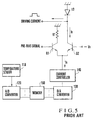
- Fig. 5 shows the arrangement of a conventional laser diode driving circuit for controlling the optical output from the laser diode.
- a laser diode LD is driven by a current prepared by superposing a driving current Id and a bias current Is.
- the driving current Id is a pulse current based on transmission data
- the bias current Is is a base current for causing the LD to emit light by induced emission.
- a temperature sensor 110 generates a voltage corresponding to the ambient temperature and outputs the voltage as an analog temperature signal representing the ambient temperature to an A/D converter 120.
- the A/D converter 120 converts the input temperature signal into a digital signal and outputs the digital signal to a memory 150.
- the memory 150 uses input digital signal as an address signal to read out digital data stored at the corresponding address from the memory 150 and output the data to a D/A converter 130.
- the D/A converter 130 converts the input digital data into an analog signal and outputs the analog signal to a current controller 140.
- the current controller 140 controls an emitter current Is common to transistors Q1 and Q2 in accordance with the analog signal from the D/A converter 130.
- a pre-bias signal is applied to the base of the transistor Q1.
- a state in which the pre-bias signal voltage is higher than a reference voltage (-VR) is a disable state.
- the disable state the transistor Q1 is turned on, the transistor Q2 is turned off, and the laser diode LD is not driven.
- the state in which the pre-bias signal voltage is lower than the reference voltage (-VR) is an enable state.
- the enable state the transistor Q1 is turned off, the transistor Q2 is turned on, and the laser diode LD is driven by a current, i.e., a current which changes between Is and Is+Id, prepared by superposing the driving current Id and the bias current Is generated by the current controller 140.
- the memory 150 data about the bias current corresponding to the ambient temperature is stored.
- data obtained by digitally converting a temperature signal representing the ambient temperature is input from the A/D converter 120 to the address line of the memory 150, the memory 150 outputs data about the bias current corresponding to the ambient temperature to the data line.
- the D/A converter 130 D/A-converts the bias current data output to the data line, and outputs the analog signal to the current controller 140.
- the current controller 140 controls the emitter current of the transistors Q1 and Q2 in accordance with the analog signal output from the D/A converter 130.
- the emitter current Is is adjusted in correspondence with the ambient temperature. That is, when the ambient temperature changes, data on the address line changes, and data about a new bias current appears on the data line.
- the D/A converter 130 D/A-converts the data on the data line, and the current controller 140 converts the signal output from the D/A converter 130 into a current.
- the laser diode LD is driven by a current prepared by superposing the driving current Id on the new bias current Is adjusted in correspondence with the ambient temperature.
- the laser diode driving circuit employs a feed forward controller. Since the circuit performs control for only optical output fluctuation conditions set in advance, it cannot control the optical output from the laser diode in correspondence with optical output fluctuation conditions other than ambient temperature fluctuations. For this reason, e.g., when the laser diode deteriorates with time to decrease the optical output, the optical output may be smaller than its lower limit defined in the optical transmission system.
- the optical output is controlled at a constant level by changing only the bias current without changing the driving current in correspondence with the ambient temperature.
- Figs. 1A and 1B show the current vs. optical output characteristics of a general laser diode.
- Fig. 1A shows current vs. optical output characteristics when the bias current and the driving current are ideally distributed.
- Fig. 1B shows current vs. optical output characteristics when the driving current is kept constant.
- the laser diode driving circuit controls the optical output Po at a constant level at the respective temperatures.
- the laser diode has such a characteristic that both the bias current Is and driving current Id required to obtain a constant optical output Po increase along with an increase in ambient temperature. As shown in Fig. 1A, it is ideal for efficiently driving the laser diode that the bias current Is is set about the light emission threshold current Ith of the laser diode, and the driving current Id is superposed on the bias current Is to keep the optical output constant.
- the bias current Is2 and the driving current Id2 are optimum at an ambient temperature t2, but the ambient temperature decreases to t1, the set value Is1 of the bias current becomes smaller than the light emission threshold current Ith1 to delay light emission. If the ambient temperature increases from t2 to t3, the set value Is3 of the bias current exceeds the light emission threshold current Ith3 to decrease the extinction ratio, failing to obtain a reliable extinction state.
- a laser diode driving method comprising the steps of adjusting, in accordance with an ambient temperature, a bias current set about a light emission threshold current of a laser diode, and a pulse current for causing the laser diode to emit light, and driving the laser diode by a current prepared by superposing the bias current and the pulse current, thereby controlling an optical output and extinction ratio of the laser diode at a constant level.
- Fig. 2 shows the arrangement of a laser diode driving circuit according to the first embodiment of the present invention.
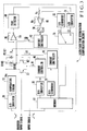
- the laser diode driving circuit of the first embodiment comprises a temperature sensor 10, A/D converters 20 and 21, D/A converters 30 to 32, current controllers 40 to 42, a memory 50, an average detector 57, an inverting amplifier 65, a low-pass filter (LPF) 70, a switch 75, an LD module 80 constituted by a laser diode 81 and a monitor photodiode (to be referred to as a monitor PD hereinafter) 82 for detecting the optical output from the laser diode 81, and transistors Q1 and Q2.
- LPF low-pass filter
- the A/D converter 21, the D/A converter 32, the current controller 42, the memory 50, the average detector 57, the inverting amplifier 65, the LPF 70, and the switch 75 constitute a laser diode time deterioration compensation circuit 1.
- the average detector 57, the inverting amplifier 65, and the LPF 70 constitute a time deterioration state detection means.
- the laser diode 81 and monitor PD 82 constituting the LD module 60 are formed on the same substrate by the same process.
- the temperature sensor 10 generates a voltage in correspondence with the ambient temperature and outputs the voltage as a temperature signal to the A/D converter 20.
- the A/D converter 20 A/D-converts the temperature signal and outputs the analog signal as an address to the memory 50.
- Data about the pulse current, the bias current, and a light-receiving current Ir of the monitor PD 82 before deterioration is stored in the memory 50 at each address corresponding to the ambient temperature.
- the values of the pulse current and bias current stored in the memory 50 are determined to keep the optical output and extinction ratio of the laser diode 81 constant against fluctuations in ambient temperature.
- the memory 50 outputs pulse current data and bias current data stored at the address designated by the A/D converter 20 to the D/A converters 30 and 31, respectively.
- the D/A converters 30 and 31 respectively D/A-convert the digital data output from the memory 50 and output the analog signals to the current controllers 40 and 41.
- the current controller 40 adjusts a constant current Iac common to the transistors Q1 and Q2 in accordance with the analog signal from the D/A converter 30.
- the current controller 41 adjusts a constant current Idc in accordance with the analog signal from the D/A converter 31.
- the light-receiving current Ir of the monitor PD 82 is input to the average detector 57.
- the average detector 57 detects the average of the light-receiving current Ir, converts it into a voltage signal, and outputs the voltage signal to the A/D converter 21 and the inverting input terminal of the inverting amplifier 65.
- the A/D converter 21 A/D-converts the input voltage from the average detector 57.
- the data digitally converted by the A/D converter 21 is output to the memory 50 via the switch 75.
- the data input from the A/D converter 21 is stored at an address corresponding to the temperature detected by the temperature sensor 10. This data serves as a reference voltage in compensating the optical output upon deterioration of the laser diode.
- the memory 50 outputs the reference voltage data to the D/A converter 32 via the switch 75.
- the D/A converter 32 D/A-converts the data and outputs the analog signal to the non-inverting input terminal of the inverting amplifier 65.
- the inverting amplifier 65 uses the voltage input from the D/A converter 32 to the non-inverting input terminal as a reference voltage to invert and amplify the voltage input from the average detector 57 to the inverting input terminal and output the voltage to the LPF 70.
- the LPF 70 smoothes the inverted/amplified voltage and outputs the resultant voltage to the current controller 42.
- the current controller 42 adjusts a constant current Iapc in accordance with the output signal from the LPF 70.
- the temperature sensor 10 detects an ambient temperature of -40 to +115 °C, converts the detected temperature into a voltage of 0 to 2 V, and outputs the voltage.
- the A/D converter 20 converts the voltage output from the temperature sensor 10 into 7-bit digital data and outputs the data as an address to the memory 50.
- the memory 50 outputs to the D/A converter 30 7-bit pulse current data stored at an address output from the A/D converter 20, and outputs to the D/A converter 31 5-bit bias current data stored at the same address.
- the D/A converter 30 D/A-converts the input digital data and outputs the analog signal to the current controller 40.
- the D/A converter 31 D/A-converts the input digital data and outputs the analog signal to the current controller 41.
- the current controller 40 adjusts the constant current Iac common to the transistors Q1 and Q2 between 0 mA and 70 mA in accordance with the analog signal from the D/A converter 30.
- An input signal to the base of the transistor Q2 is a signal based on transmission data
- an inverted input signal to the base of the transistor Q1 is a signal obtained by inverting the input signal.
- the transistor Q2 When the input signal is at high level, the transistor Q2 is turned on, the transistor Q1 is turned off, and the constant current Iac flows through the laser diode 81.
- the transistor Q1 When the input signal is at low level, the transistor Q1 is turned on, the transistor Q2 is turned off, and no constant current Iac flows through the laser diode 81. That is, the constant current Iac drives the laser diode 81 as a pulse current based on transmission data.
- the current controller 41 adjusts the constant current Idc between 0 mA and 50 mA in accordance with the analog signal from the D/A converter 31.
- the constant current Idc directly flows through the laser diode 81 and drives it as a bias current.
- the operation of the laser diode time deterioration compensation circuit 1 will be explained.
- the light-receiving current Ir of the monitor PD 82 is input to the average detector 57.
- the average detector 57 detects the average of the light-receiving current Ir, converts it into a voltage of 0 to 550 mV, and outputs the voltage to the A/D converter 21 and the inverting input terminal of the inverting amplifier 65.
- the A/D converter 21 converts the voltage output from the average detector 57 into 5-bit digital data.
- the data digitally converted by the A/D converter 21 is output to the memory 50 via the switch 75.
- the data input from the A/D converter 21 is stored at an address corresponding to the temperature detected by the temperature sensor 10. This data is used as an initial output value of the monitor PD, i.e., reference voltage data before deterioration of the laser diode 81.
- the memory 50 outputs the reference voltage data to the D/A converter 32 via the switch 75.
- the D/A converter 32 converts the reference voltage data into a voltage of 0 to 550 mV and outputs the voltage to the non-inverting input terminal of the inverting amplifier 65.
- the switch 75 connects either the A/D converter 21 or the D/A converter 32 to the memory 50.
- the switch 75 switches to the A/D converter 21 side (2 ⁇ ) in writing the reference voltage data in the memory 50, and to the D/A converter 32 side (1 ⁇ ) in reading out the reference voltage data from the memory 50.
- the inverting amplifier 65 uses the voltage input from the D/A converter 32 to the non-inverting input terminal as a reference voltage to invert and amplify the voltage input from the average detector 57 to the inverting input terminal and output the voltage to the LPF 70.
- the LPF 70 smoothes the inverted/amplified voltage and outputs the resultant voltage to the current controller 42.
- the current controller 42 adjusts the constant current Iapc between 0 mA and 30 mA in accordance with the output signal from the LPF 70.
- the constant current Iapc directly flows through the laser diode 81 and drives it as a bias current, similarly to the constant current Idc. That is, the current controller 42 adjusts the constant current Iapc in correspondence with a decrease in light-receiving current Ir of the monitor PD 82 caused by deterioration of the laser diode 81 over time. A decrease in bias current caused by deterioration of the laser diode 81 over time is compensated up to 30 mA by the constant current Iapc.
- the optical output fluctuating upon deterioration of the laser diode 81 over time is controlled at a constant level. More specifically, data about the light-receiving current Ir of the monitor PD 82 when the laser diode 81 before deterioration outputs a desired light power is stored in the memory 50 for each temperature. The initial data stored in the memory 50 is used as a reference value. A decrease in light-receiving current Ir of the monitor PD 82 is detected as a decrease in optical output from the laser diode 81 on the basis of the reference value, and feedback control for increasing the bias current is performed. Accordingly, the optical output can be compensated by an amount corresponding to deterioration of the laser diode 81, and the optical output can be controlled at a constant level.
- the measured data of the light-receiving current Ir is used as a reference value, which includes variations in an individual laser diode and another device. Therefore, the optical output and the extinction ratio can be controlled without any special adjustment for the time deterioration compensation circuit 1.
- the bias current and the pulse current can be independently controlled in correspondence with the ambient temperature. More specifically, the bias current and the pulse current are stored in the memory 50 at an address corresponding to the ambient temperature. The bias current and pulse current corresponding to the ambient temperature drive the laser diode 81.
- the bias current and the pulse current can be independently controlled, not only the optical output but also the extinction ratio can be controlled at a constant level in correspondence with the ambient temperature by storing the bias current and the pulse current in the memory 50 in accordance with the current vs. optical output characteristics of each laser diode 81 for each temperature.
- the laser diode driving circuit can drive the laser diode suitably for the transmission system without any light emission delay and any failure to obtain a reliable extinction state due to a decrease in extinction ratio.
- Fig. 3 shows the arrangement of a laser diode driving circuit according to the second embodiment of the present invention.
- the laser diode driving circuit of the second embodiment comprises a preamplifier 55 and a peak detector 60 instead of the average detector 57 in the first embodiment shown in Fig. 2. Since the remaining arrangement is the same as in the first embodiment shown in Fig. 2, the same reference numerals as in Fig. 2 denote the same parts, and a description thereof will be omitted.
- a light-receiving current Ir of a monitor PD 82 is input to the preamplifier 55 and converted into a voltage signal.
- the voltage signal is output to the peak detector 60.
- the peak detector 60 detects the peak voltage of the voltage signal output from the preamplifier 55, and outputs the detection voltage to an A/D converter 21 and the inverting input terminal of an inverting amplifier 65. The remaining operation is the same as in the first embodiment.
- deterioration of the laser diode 81 over time is compensated based on the average of the light-receiving current Ir of the monitor PD 82.
- deterioration of the laser diode 81 over time is compensated based on the peak value of the light-receiving current Ir of the monitor PD 82.
- the average of the light-receiving current Ir of the monitor PD 82 is very low, and fluctuations in light-receiving current Ir of the monitor PD 82 are difficult to detect. For this reason, deterioration of the laser diode 81 cannot be determined.
- the peak value of the light-receiving current Ir of the monitor PD 82 is detected, even if a burst signal is used as transmission data, deterioration of the laser diode 81 over time can be determined, and a decrease in optical output can be compensated in correspondence with a decrease in peak value.
- Fig. 4 shows the arrangement of a laser diode driving circuit according to the third embodiment of the present invention.
- the laser diode driving circuit of the third embodiment has the same constituent elements as in the second embodiment shown in Fig. 3 except that a current controller 42 controls two different constant currents, i.e., a constant current Iapc1 and a constant current Iapc2. Since the remaining arrangement is the same as in the second embodiment shown in Fig. 3, the same reference numerals as in Fig. 3 denote the same parts, and a description thereof will be omitted.
- the constant current Iapc1 serves as a bias current directly flowing through a laser diode 81, whereas the constant current Iapc2 serves as a pulse current controlled by an input signal.
- both the bias current and the pulse current are compensated in accordance with deterioration of the laser diode 81 over time.
- the optical output and the extinction ratio can be controlled at a constant level in correspondence with deterioration of the laser diode 81 over time.
- the third embodiment adopts the preamplifier 55 and the peak detector 60.
- an average detector 57 may replace the preamplifier 55 and the peak detector 60, and deterioration of a laser diode 81 over time may be compensated based on the average of the light-receiving current Ir of a monitor PD 82, similarly to the first embodiment.
Landscapes
- Physics & Mathematics (AREA)
- Condensed Matter Physics & Semiconductors (AREA)
- General Physics & Mathematics (AREA)
- Electromagnetism (AREA)
- Optics & Photonics (AREA)
- Semiconductor Lasers (AREA)
Abstract
Description
Claims (11)
- A laser diode driving method characterized by comprising the steps of:adjusting, in accordance with an ambient temperature, a bias current set about a light emission threshold current of a laser diode (81), and a pulse current for causing the laser diode to emit light; anddriving the laser diode by a current prepared by superposing the bias current (Idc) and the pulse current (Iac), thereby controlling an optical output and extinction ratio of the laser diode at a constant level.
- A laser diode driving method comprising the steps of:adjusting, in accordance with an ambient temperature, a bias current set about a light emission threshold current of a laser diode (81), and a pulse current for causing the laser diode to emit light;adjusting the bias current in accordance with a deterioration state of the laser diode over time; anddriving the laser diode by a current prepared by superposing the bias current (Idc, Iapc) and the pulse current (Iac), thereby controlling an optical output of the laser diode at a constant level.
- A laser diode driving method comprising the steps of:adjusting, in accordance with an ambient temperature and a deterioration state of a laser diode (81) over time, a bias current set about a light emission threshold current of the laser diode, and a pulse current for causing the laser diode to emit light; anddriving the laser diode by a current prepared by superposing the bias current (Idc, Iapc1) and the pulse current (Iac, Iapc2), thereby controlling an optical output and extinction ratio of the laser diode at a constant level.
- A method according to claim 2 or 3, wherein the deterioration state of the laser diode (81) with time is confirmed using an average of outputs of a monitor photodiode (82) for detecting the optical output of the laser diode.
- A method according to claim 2 or 3, wherein the deterioration state of the laser diode (81) with time is confirmed using a peak value of outputs of a monitor photodiode (82) for detecting the optical output of the laser diode.
- A method according to claim 2, 3, 4 or 5 further comprising the steps of:storing, in correspondence with ambient temperatures, initial output values of a monitor photodiode (82) for detecting the optical output of the laser diode (81);obtaining an initial output value corresponding to a current ambient temperature from the stored output values; andcomparing the initial output value with a current output value of the monitor photodiode, thereby confirming the deterioration state of the laser diode over time.
- A laser diode driving circuit comprising:a laser diode (81);a temperature sensor (10) for detecting an ambient temperature;memory means (50) for storing, in correspondence with ambient temperatures, bias current values set about a light emission threshold current of said laser diode, and pulse current values for causing said laser diode to emit light, and outputting a bias current value and pulse current value corresponding to an ambient temperature detected by said temperature sensor; andcurrent control means (40, 41) for determining a bias current (Idc) and pulse current (Iac) for said laser diode on the basis of the values output from said memory means, and driving said laser diode by a current prepared by superposing the bias current and the pulse current.
- A laser diode driving circuit comprising:a laser diode (81);a temperature sensor (10) for detecting an ambient temperature;a monitor photodiode (82) for detecting an optical output of said laser diode;memory means (50) for storing, in correspondence with ambient temperatures, bias current values set about a light emission threshold current of said laser diode, pulse current values for causing said laser diode to emit light, and initial output values of said monitor photodiodes, and outputting a bias current value, pulse current value, and initial output value of said monitor photodiode corresponding to an ambient temperature detected by said temperature sensor;time deterioration state detection means (55, 57, 60, 65, 70) for comparing the initial output value of said monitor photodiode output from said memory means with a current output value, and generating a signal representing a deterioration state of said laser diode over time; andcurrent control means (40, 41, 42) for determining a pulse current (Iac) for said laser diode on the basis of the pulse current value output from said memory means, determining a bias current (Idc, Iac) for said laser diode on the basis of the bias current value output from said memory means and the signal representing the deterioration state over time output from said time deterioration state detection means, and driving said laser diode by a current prepared by superposing the bias current and the pulse current.
- A laser diode driving circuit comprising:a laser diode (81);a temperature sensor (10) for detecting an ambient temperature;a monitor photodiode (82) for detecting an optical output of said laser diode;memory means (50) for storing, in correspondence with ambient temperatures, bias current values set about a light emission threshold current of said laser diode, pulse current values for causing said laser diode to emit light, and initial output values of said monitor photodiodes, and outputting a bias current value, pulse current value, and initial output value of said monitor photodiode corresponding to an ambient temperature detected by said temperature sensor;time deterioration state detection means (55, 57, 60, 65, 70) for comparing the initial output value of said monitor photodiode output from said memory means with a current output value, and generating a signal representing a deterioration state of said laser diode over time; andcurrent control means (40, 41, 42) for determining a bias current (Idc, Iapc1) and pulse current (Iac, Iapc2) for said laser diode on the basis of the bias current value and pulse current value output from said memory means and the signal representing the deterioration state over time output from said time deterioration state detection means, and driving said laser diode by a current prepared by superposing the bias current and the pulse current.
- A circuit according to claim 7, 8 or 9, wherein said memory means stores an average of the initial outputs of said monitor photodiode, andsaid time deterioration state detection means comprises an average detector for detecting an average of current outputs of said monitor photodiode.
- A circuit according to claim 7, 8 or 9, wherein said memory means stores a peak value of the initial outputs of said monitor photodiode, andsaid time deterioration state detection means comprises a peak detector for detecting a peak value of current outputs of said monitor photodiode.
Applications Claiming Priority (3)
| Application Number | Priority Date | Filing Date | Title |
|---|---|---|---|
| JP29574697A JPH11135871A (en) | 1997-10-28 | 1997-10-28 | Method for activating laser diode and circuit thereof |
| JP295746/97 | 1997-10-28 | ||
| JP29574697 | 1997-10-28 |
Publications (3)
| Publication Number | Publication Date |
|---|---|
| EP0913896A2 true EP0913896A2 (en) | 1999-05-06 |
| EP0913896A3 EP0913896A3 (en) | 2002-04-03 |
| EP0913896B1 EP0913896B1 (en) | 2004-02-11 |
Family
ID=17824634
Family Applications (1)
| Application Number | Title | Priority Date | Filing Date |
|---|---|---|---|
| EP19980120149 Expired - Lifetime EP0913896B1 (en) | 1997-10-28 | 1998-10-27 | Laser diode driving method and circuit |
Country Status (4)
| Country | Link |
|---|---|
| US (1) | US6292497B1 (en) |
| EP (1) | EP0913896B1 (en) |
| JP (1) | JPH11135871A (en) |
| DE (1) | DE69821572T2 (en) |
Cited By (14)
| Publication number | Priority date | Publication date | Assignee | Title |
|---|---|---|---|---|
| EP1345296A1 (en) * | 2002-03-16 | 2003-09-17 | Agilent Technologies, Inc. (a Delaware corporation) | System for controlling power, wavelength and extinction ratio in optical sources, and computer program product therefor |
| EP1376557A1 (en) * | 2002-06-26 | 2004-01-02 | Hitachi-LG Data Storage Korea Inc. | Method for controlling an optical power level |
| GB2397169A (en) * | 2003-01-10 | 2004-07-14 | Agilent Technologies Inc | Laser Systems |
| EP1391971A3 (en) * | 2002-08-21 | 2005-06-01 | Siemens Aktiengesellschaft | Device and procedure to reduce the settling time of a laser |
| GB2412025A (en) * | 2002-11-08 | 2005-09-14 | Finisar Corp | Temperature and jitter compensation controller circuit and method for fiber optics device |
| US6947457B2 (en) | 2000-02-14 | 2005-09-20 | Yokogawa Electric Corporation | DFB laser driving device, DFB laser driving method and storage medium |
| EP1472644A4 (en) * | 2002-01-14 | 2005-09-28 | Ceyx Technologies Inc | Laser temperature performance compensation |
| EP1485736A4 (en) * | 2002-02-12 | 2006-01-11 | Finisar Corp | Maintaining desirable performance of optical emitters at extreme temperatures |
| EP1282207A4 (en) * | 2001-02-23 | 2006-08-09 | Fujitsu Ltd | LIGHT EMITTER |
| EP1788413A3 (en) * | 2002-02-12 | 2007-06-13 | Finisar Corporation | Maintaining desirable performance of optical emitters at extreme temperatures |
| CN101447642B (en) * | 2007-11-30 | 2010-12-08 | 株式会社理光 | Semiconductor device, semiconductor laser driving device and image forming device |
| EP1352286B1 (en) * | 2000-11-03 | 2011-05-04 | Microvision, Inc. | Scanned display with variation compensation |
| EP2312911A3 (en) * | 2009-09-17 | 2012-05-23 | Dialog Semiconductor GmbH | Circuit for driving an infrared transmitter LED dependent on the temperature |
| EP2180564A4 (en) * | 2007-08-13 | 2015-06-24 | Omron Tateisi Electronics Co | Semiconductor laser drive apparatus, semiconductor laser drive method, optical transmitter, optical wiring module, and electronic device |
Families Citing this family (73)
| Publication number | Priority date | Publication date | Assignee | Title |
|---|---|---|---|---|
| SE519081C3 (en) * | 1998-01-21 | 2003-02-19 | Altitun Ab | Method and apparatus for optimizing the laser operating point and device |
| JP3668612B2 (en) * | 1998-06-29 | 2005-07-06 | 株式会社東芝 | Optical semiconductor device drive circuit and optical transceiver module |
| SE518827C2 (en) | 1999-02-17 | 2002-11-26 | Altitun Ab | Method for characterizing a tunable laser |
| US6671248B2 (en) * | 2000-05-18 | 2003-12-30 | Matsushita Electric Industrial Co., Ltd. | Apparatus and method of controlling laser power |
| JP3729045B2 (en) * | 2000-08-30 | 2005-12-21 | 日本電気株式会社 | Optical module abnormality detection method and apparatus |
| WO2002037622A2 (en) | 2000-11-06 | 2002-05-10 | Vitesse Semiconductor Corporation | Method of controlling the turn off characteristics of a vcsel diode |
| JP2002217836A (en) * | 2001-01-15 | 2002-08-02 | Oki Electric Ind Co Ltd | Laser diode drive circuit and optical transmission system |
| JP3637872B2 (en) | 2001-02-08 | 2005-04-13 | 日本電気株式会社 | Laser diode drive circuit and method with feedforward type APC circuit |
| US6993459B2 (en) * | 2001-07-17 | 2006-01-31 | Tellabs Operations, Inc. | Extinction ratio calculation and control of a laser |
| EP1413024B1 (en) * | 2001-08-03 | 2004-12-29 | Infineon Technologies AG | Method and device for adjusting a laser |
| US6975642B2 (en) | 2001-09-17 | 2005-12-13 | Finisar Corporation | Optoelectronic device capable of participating in in-band traffic |
| JP3748432B2 (en) * | 2001-12-20 | 2006-02-22 | 株式会社東芝 | LIGHT EMITTING DEVICE CONTROL DEVICE, OPTICAL TRANSMITTER, DRIVE CURRENT DETERMINING METHOD, AND PROGRAM |
| EP1470522A4 (en) * | 2001-12-27 | 2005-10-05 | Ceyx Technologies Inc | Laser optics integrated control system and method of operation |
| US6862302B2 (en) * | 2002-02-12 | 2005-03-01 | Finisar Corporation | Maintaining desirable performance of optical emitters over temperature variations |
| US20030161592A1 (en) * | 2002-02-27 | 2003-08-28 | Optronx, Inc. | Header with temperature sensor positioned proximate the laser |
| US6873632B2 (en) * | 2002-05-22 | 2005-03-29 | Finisar Corporation | Techniques for biasing lasers |
| US6885685B2 (en) * | 2002-06-11 | 2005-04-26 | Sumitomo Electric Industries, Ltd. | Control system for a laser diode and a method for controlling the same |
| US7809275B2 (en) * | 2002-06-25 | 2010-10-05 | Finisar Corporation | XFP transceiver with 8.5G CDR bypass |
| US7561855B2 (en) | 2002-06-25 | 2009-07-14 | Finisar Corporation | Transceiver module and integrated circuit with clock and data recovery clock diplexing |
| US7437079B1 (en) | 2002-06-25 | 2008-10-14 | Finisar Corporation | Automatic selection of data rate for optoelectronic devices |
| US7486894B2 (en) | 2002-06-25 | 2009-02-03 | Finisar Corporation | Transceiver module and integrated circuit with dual eye openers |
| US7664401B2 (en) | 2002-06-25 | 2010-02-16 | Finisar Corporation | Apparatus, system and methods for modifying operating characteristics of optoelectronic devices |
| US7477847B2 (en) * | 2002-09-13 | 2009-01-13 | Finisar Corporation | Optical and electrical channel feedback in optical transceiver module |
| JP2004111827A (en) * | 2002-09-20 | 2004-04-08 | Alps Electric Co Ltd | Optical output control circuit of semiconductor laser |
| US7230961B2 (en) | 2002-11-08 | 2007-06-12 | Finisar Corporation | Temperature and jitter compensation controller circuit and method for fiber optics device |
| US20040131094A1 (en) * | 2002-12-18 | 2004-07-08 | Reza Miremadi | Method of controlling the extinction ratio of a laser |
| US7043997B2 (en) * | 2003-07-09 | 2006-05-16 | Cherry Corporation | Seat for sensing a load |
| US7426586B2 (en) * | 2003-12-15 | 2008-09-16 | Finisar Corporation | Configurable input/output terminals |
| US20050180711A1 (en) * | 2004-02-13 | 2005-08-18 | Kamath Kishore K. | Dual loop automatic power control of optical transmitters |
| US7266136B2 (en) * | 2004-03-25 | 2007-09-04 | Finisar Corporation | Temperature compensation for fiber optic transceivers using optimized convergence algorithms |
| US7630631B2 (en) * | 2004-04-14 | 2009-12-08 | Finisar Corporation | Out-of-band data communication between network transceivers |
| US20050271099A1 (en) * | 2004-06-04 | 2005-12-08 | Optical Communication Products, Inc. | Burst mode transmitter system |
| US7447438B2 (en) | 2004-07-02 | 2008-11-04 | Finisar Corporation | Calibration of digital diagnostics information in an optical transceiver prior to reporting to host |
| US8639122B2 (en) | 2004-07-02 | 2014-01-28 | Finisar Corporation | Filtering digital diagnostics information in an optical transceiver prior to reporting to host |
| US7352784B2 (en) * | 2004-07-20 | 2008-04-01 | Jds Uniphase Corporation | Laser burst boosting method and apparatus |
| US7132805B2 (en) * | 2004-08-09 | 2006-11-07 | Dialight Corporation | Intelligent drive circuit for a light emitting diode (LED) light engine |
| US7504610B2 (en) * | 2004-09-03 | 2009-03-17 | Mindspeed Technologies, Inc. | Optical modulation amplitude compensation system having a laser driver with modulation control signals |
| JP2006080677A (en) * | 2004-09-07 | 2006-03-23 | Sumitomo Electric Ind Ltd | Optical data link |
| US7532820B2 (en) | 2004-10-29 | 2009-05-12 | Finisar Corporation | Systems and methods for providing diagnostic information using EDC transceivers |
| US20060126684A1 (en) * | 2004-12-10 | 2006-06-15 | Chien-Chang Liu | Real time constant excitation ratio (ER) laser driving circuit |
| US7242701B2 (en) * | 2005-02-15 | 2007-07-10 | Lucent Technologies Inc. | Laser wavelength control arrangement and method |
| US20070116076A1 (en) * | 2005-11-21 | 2007-05-24 | Frank Wang | Controlling optical power and extincation ratio of a semiconductor laser |
| US20070160374A1 (en) * | 2005-12-20 | 2007-07-12 | Fujitsu Limited | Optical transmitter and method for controlling optical transmitter |
| US7403214B2 (en) * | 2006-02-21 | 2008-07-22 | Lexmark International, Inc. | Systems and methods for adjusting the dynamic range of a scanning laser beam |
| JP2007324525A (en) * | 2006-06-05 | 2007-12-13 | Fuji Xerox Co Ltd | Optical transmitter, optical communication system, and adjustment method for optical transmitter |
| JP4574650B2 (en) * | 2007-07-09 | 2010-11-04 | キヤノン株式会社 | Laser diode driving device and optical scanning device |
| JP2009070879A (en) * | 2007-09-11 | 2009-04-02 | Nec Corp | Laser diode drive circuit and drive method |
| US7711018B2 (en) * | 2007-12-21 | 2010-05-04 | Microvision, Inc. | Method and apparatus for laser diode compensation |
| US8750341B2 (en) * | 2008-01-04 | 2014-06-10 | Mindspeed Technologies, Inc. | Method and apparatus for reducing optical signal speckle |
| JP5166060B2 (en) * | 2008-02-08 | 2013-03-21 | 富士通テレコムネットワークス株式会社 | Laser diode pulse current control method and operating current control apparatus thereof |
| KR101623996B1 (en) | 2008-03-31 | 2016-05-24 | 마인드스피드 테크놀로지 인크 | Reducing power dissipation in portable lcos/lcd/dlp projection systems |
| TWI408725B (en) * | 2008-12-04 | 2013-09-11 | Ind Tech Res Inst | Electron emission device and package method thereof |
| JP5439970B2 (en) | 2009-06-18 | 2014-03-12 | 住友電気工業株式会社 | Laser diode driving method and optical transmitter |
| JP5749458B2 (en) * | 2010-07-21 | 2015-07-15 | 富士通オプティカルコンポーネンツ株式会社 | Optical transmission module and method for controlling optical transmission module |
| US8643296B2 (en) | 2010-11-22 | 2014-02-04 | Mindspeed Technologies, Inc. | Color mixing and desaturation with reduced number of converters |
| US9000934B1 (en) | 2010-12-17 | 2015-04-07 | Musco Corporation | Apparatus, method, and system for determining end-of-life of a product |
| JP2012142417A (en) | 2010-12-28 | 2012-07-26 | Sumitomo Electric Device Innovations Inc | Control method of laser diode |
| CN103392094B (en) | 2011-02-25 | 2016-12-21 | 玛斯柯有限公司 | Compact adjustable LED light device and the method and system of longtime running |
| US9107245B2 (en) | 2011-06-09 | 2015-08-11 | Mindspeed Technologies, Inc. | High accuracy, high dynamic range LED/laser driver |
| US8872487B2 (en) | 2011-08-28 | 2014-10-28 | Mindspeed Technologies, Inc. | Scalable buck-boost DC-DC converter |
| US9385606B2 (en) | 2012-12-03 | 2016-07-05 | M/A-Com Technology Solutions Holdings, Inc. | Automatic buck/boost mode selection system for DC-DC converter |
| US10097908B2 (en) | 2014-12-31 | 2018-10-09 | Macom Technology Solutions Holdings, Inc. | DC-coupled laser driver with AC-coupled termination element |
| WO2018045093A1 (en) | 2016-08-30 | 2018-03-08 | Macom Technology Solutions Holdings, Inc. | Driver with distributed architecture |
| US10630052B2 (en) | 2017-10-04 | 2020-04-21 | Macom Technology Solutions Holdings, Inc. | Efficiency improved driver for laser diode in optical communication |
| EP3804247B1 (en) | 2018-05-30 | 2024-08-14 | MACOM Technology Solutions Holdings, Inc. | Integrated circuit based ac coupling topology |
| US11005573B2 (en) | 2018-11-20 | 2021-05-11 | Macom Technology Solutions Holdings, Inc. | Optic signal receiver with dynamic control |
| US11438064B2 (en) | 2020-01-10 | 2022-09-06 | Macom Technology Solutions Holdings, Inc. | Optimal equalization partitioning |
| US11575437B2 (en) | 2020-01-10 | 2023-02-07 | Macom Technology Solutions Holdings, Inc. | Optimal equalization partitioning |
| US12013423B2 (en) | 2020-09-30 | 2024-06-18 | Macom Technology Solutions Holdings, Inc. | TIA bandwidth testing system and method |
| US11658630B2 (en) | 2020-12-04 | 2023-05-23 | Macom Technology Solutions Holdings, Inc. | Single servo loop controlling an automatic gain control and current sourcing mechanism |
| US11616529B2 (en) | 2021-02-12 | 2023-03-28 | Macom Technology Solutions Holdings, Inc. | Adaptive cable equalizer |
| US12395130B2 (en) | 2022-12-27 | 2025-08-19 | Macom Technology Solutions Holdings, Inc. | Variable gain optical modulator with open collector driver amplifier and method of operation |
| US12567847B2 (en) | 2022-12-27 | 2026-03-03 | Macom Technology Solutions Holdings, Inc. | Variable gain optical modulator with open collector driver amplifier and method of operation |
Family Cites Families (11)
| Publication number | Priority date | Publication date | Assignee | Title |
|---|---|---|---|---|
| JPS59112670A (en) | 1982-12-20 | 1984-06-29 | Hitachi Ltd | Output stabilizing circuit for optical digital transmitter |
| JPS60251731A (en) | 1984-05-29 | 1985-12-12 | Fujitsu Ltd | Optical output controller |
| JP2507387B2 (en) * | 1987-02-13 | 1996-06-12 | 株式会社東芝 | Power converter |
| JPH02308584A (en) * | 1989-05-24 | 1990-12-21 | Toshiba Corp | Light output control circuit of laser diode |
| JPH0356871A (en) | 1989-07-24 | 1991-03-12 | Nec Corp | Deterioration detection circuit |
| JP2546080B2 (en) * | 1991-05-10 | 1996-10-23 | 富士通株式会社 | Semiconductor laser control device |
| US5278404A (en) * | 1992-07-20 | 1994-01-11 | At&T Bell Laboratories | Optical sub-system utilizing an embedded micro-controller |
| DE4316811A1 (en) * | 1993-05-19 | 1994-11-24 | Philips Patentverwaltung | Optical transmission system with a laser diode |
| JP3596963B2 (en) * | 1995-12-06 | 2004-12-02 | 株式会社ルネサステクノロジ | Semiconductor device mounted module, optical transmitter, method for creating characteristic information of laser diode, and optical transmission device |
| US5812572A (en) * | 1996-07-01 | 1998-09-22 | Pacific Fiberoptics, Inc. | Intelligent fiberoptic transmitters and methods of operating and manufacturing the same |
| US6055252A (en) * | 1998-09-10 | 2000-04-25 | Photonic Solutions, Inc. | Fiberoptic transmitter using thermistor to maintain stable operating conditions over a range of temperature |
-
1997
- 1997-10-28 JP JP29574697A patent/JPH11135871A/en active Pending
-
1998
- 1998-10-27 US US09/179,561 patent/US6292497B1/en not_active Expired - Fee Related
- 1998-10-27 EP EP19980120149 patent/EP0913896B1/en not_active Expired - Lifetime
- 1998-10-27 DE DE1998621572 patent/DE69821572T2/en not_active Expired - Lifetime
Cited By (21)
| Publication number | Priority date | Publication date | Assignee | Title |
|---|---|---|---|---|
| US6947457B2 (en) | 2000-02-14 | 2005-09-20 | Yokogawa Electric Corporation | DFB laser driving device, DFB laser driving method and storage medium |
| EP1352286B1 (en) * | 2000-11-03 | 2011-05-04 | Microvision, Inc. | Scanned display with variation compensation |
| EP1282207A4 (en) * | 2001-02-23 | 2006-08-09 | Fujitsu Ltd | LIGHT EMITTER |
| EP1472644A4 (en) * | 2002-01-14 | 2005-09-28 | Ceyx Technologies Inc | Laser temperature performance compensation |
| EP1485736A4 (en) * | 2002-02-12 | 2006-01-11 | Finisar Corp | Maintaining desirable performance of optical emitters at extreme temperatures |
| EP1788413A3 (en) * | 2002-02-12 | 2007-06-13 | Finisar Corporation | Maintaining desirable performance of optical emitters at extreme temperatures |
| EP1345296A1 (en) * | 2002-03-16 | 2003-09-17 | Agilent Technologies, Inc. (a Delaware corporation) | System for controlling power, wavelength and extinction ratio in optical sources, and computer program product therefor |
| EP1376557A1 (en) * | 2002-06-26 | 2004-01-02 | Hitachi-LG Data Storage Korea Inc. | Method for controlling an optical power level |
| US7414934B2 (en) | 2002-06-26 | 2008-08-19 | Hitachi-Lg Data Storage Korea, Inc. | Method for controlling optical power level |
| EP1391971A3 (en) * | 2002-08-21 | 2005-06-01 | Siemens Aktiengesellschaft | Device and procedure to reduce the settling time of a laser |
| GB2423879A (en) * | 2002-11-08 | 2006-09-06 | Finisar Corp | Temperature controller for optical device |
| GB2412025B (en) * | 2002-11-08 | 2006-06-28 | Finisar Corp | Temperature and jitter compensation controller circuit and method for fiber optics device |
| GB2423879B (en) * | 2002-11-08 | 2007-10-10 | Finisar Corp | Temperature and jitter compensation controller circuit and method for fiber optics device |
| GB2412025A (en) * | 2002-11-08 | 2005-09-14 | Finisar Corp | Temperature and jitter compensation controller circuit and method for fiber optics device |
| GB2397169B (en) * | 2003-01-10 | 2007-05-16 | Agilent Technologies Inc | Laser systems |
| US7830936B2 (en) | 2003-01-10 | 2010-11-09 | Avago Technologies Fiber Ip (Singapore) Pte. Ltd. | Calibration of laser systems |
| GB2397169A (en) * | 2003-01-10 | 2004-07-14 | Agilent Technologies Inc | Laser Systems |
| EP2180564A4 (en) * | 2007-08-13 | 2015-06-24 | Omron Tateisi Electronics Co | Semiconductor laser drive apparatus, semiconductor laser drive method, optical transmitter, optical wiring module, and electronic device |
| CN101447642B (en) * | 2007-11-30 | 2010-12-08 | 株式会社理光 | Semiconductor device, semiconductor laser driving device and image forming device |
| EP2312911A3 (en) * | 2009-09-17 | 2012-05-23 | Dialog Semiconductor GmbH | Circuit for driving an infrared transmitter LED dependent on the temperature |
| US8283876B2 (en) | 2009-09-17 | 2012-10-09 | Dialog Semiconductor Gmbh | Circuit for driving an infrared transmitter LED with temperature compensation |
Also Published As
| Publication number | Publication date |
|---|---|
| EP0913896B1 (en) | 2004-02-11 |
| EP0913896A3 (en) | 2002-04-03 |
| US6292497B1 (en) | 2001-09-18 |
| DE69821572T2 (en) | 2004-12-16 |
| JPH11135871A (en) | 1999-05-21 |
| DE69821572D1 (en) | 2004-03-18 |
Similar Documents
| Publication | Publication Date | Title |
|---|---|---|
| EP0913896B1 (en) | Laser diode driving method and circuit | |
| CA2284259C (en) | Laser modulation control method and apparatus | |
| EP0660471B1 (en) | Current driven voltage sensed laser diode driver (CDVS LDD) | |
| US20040028099A1 (en) | Drive circuit and drive method of semiconductor laser module provided with electro-absorption type optical modulator | |
| US20010020670A1 (en) | Automatic power control circuit | |
| US5036519A (en) | Semiconductor laser controller | |
| US7760780B2 (en) | Laser diode driving device and optical scanning device | |
| US20030016426A1 (en) | Apparatus and method for detecting beam power in optical drive | |
| US20050046448A1 (en) | Current-voltage transforming circuit employing limiter circuit | |
| US20040190569A1 (en) | Apparatus for compensating for characteristics of laser diode and optical transmitter including the apparatus | |
| US6560258B1 (en) | Direct-coupled laser diode driver structures and methods | |
| US20020093999A1 (en) | Laser diode drive circuit and optical transmission system | |
| JPH09214043A (en) | Optical transmitting circuit | |
| KR20200110986A (en) | Controller of optical transmitter | |
| JP2005057216A (en) | Laser diode drive circuit and optical transmitter | |
| US6466594B1 (en) | Laser modulating device | |
| US6445401B2 (en) | Light power modulating system | |
| JPH02205086A (en) | Semiconductor laser control device | |
| JP4810787B2 (en) | Light emitting element driving device and image forming apparatus | |
| JP4830606B2 (en) | Optical output control circuit, optical communication device, optical output control method, and optical output control program | |
| KR100268466B1 (en) | Optical power adjusting device according to RF level of optical disc player | |
| JPS61224385A (en) | Semiconductor laser drive circuit | |
| JP2009070879A (en) | Laser diode drive circuit and drive method | |
| JP3463741B2 (en) | Optical output stabilization device for integrated semiconductor laser array | |
| JPH04129284A (en) | Laser diode drive circuit |
Legal Events
| Date | Code | Title | Description |
|---|---|---|---|
| PUAI | Public reference made under article 153(3) epc to a published international application that has entered the european phase |
Free format text: ORIGINAL CODE: 0009012 |
|
| AK | Designated contracting states |
Kind code of ref document: A2 Designated state(s): AT BE CH CY DE DK ES FI FR GB GR IE IT LI LU MC NL PT SE Kind code of ref document: A2 Designated state(s): DE FR GB |
|
| AX | Request for extension of the european patent |
Free format text: AL;LT;LV;MK;RO;SI |
|
| PUAL | Search report despatched |
Free format text: ORIGINAL CODE: 0009013 |
|
| AK | Designated contracting states |
Kind code of ref document: A3 Designated state(s): AT BE CH CY DE DK ES FI FR GB GR IE IT LI LU MC NL PT SE |
|
| AX | Request for extension of the european patent |
Free format text: AL;LT;LV;MK;RO;SI |
|
| RIC1 | Information provided on ipc code assigned before grant |
Free format text: 7H 01S 3/096 A, 7H 01S 3/133 B, 7H 01S 5/042 B, 7H 01S 5/068 B |
|
| 17P | Request for examination filed |
Effective date: 20020226 |
|
| 17Q | First examination report despatched |
Effective date: 20020709 |
|
| AKX | Designation fees paid |
Free format text: DE FR GB |
|
| RIC1 | Information provided on ipc code assigned before grant |
Ipc: 7H 01S 5/068 B Ipc: 7H 01S 5/042 A |
|
| RIC1 | Information provided on ipc code assigned before grant |
Ipc: 7H 01S 5/068 B Ipc: 7H 01S 5/042 A |
|
| GRAP | Despatch of communication of intention to grant a patent |
Free format text: ORIGINAL CODE: EPIDOSNIGR1 |
|
| GRAS | Grant fee paid |
Free format text: ORIGINAL CODE: EPIDOSNIGR3 |
|
| GRAA | (expected) grant |
Free format text: ORIGINAL CODE: 0009210 |
|
| AK | Designated contracting states |
Kind code of ref document: B1 Designated state(s): DE FR GB |
|
| REG | Reference to a national code |
Ref country code: GB Ref legal event code: FG4D |
|
| REG | Reference to a national code |
Ref country code: IE Ref legal event code: FG4D |
|
| REF | Corresponds to: |
Ref document number: 69821572 Country of ref document: DE Date of ref document: 20040318 Kind code of ref document: P |
|
| ET | Fr: translation filed | ||
| PLBE | No opposition filed within time limit |
Free format text: ORIGINAL CODE: 0009261 |
|
| STAA | Information on the status of an ep patent application or granted ep patent |
Free format text: STATUS: NO OPPOSITION FILED WITHIN TIME LIMIT |
|
| 26N | No opposition filed |
Effective date: 20041112 |
|
| PGFP | Annual fee paid to national office [announced via postgrant information from national office to epo] |
Ref country code: DE Payment date: 20091022 Year of fee payment: 12 |
|
| PGFP | Annual fee paid to national office [announced via postgrant information from national office to epo] |
Ref country code: GB Payment date: 20091021 Year of fee payment: 12 Ref country code: FR Payment date: 20091029 Year of fee payment: 12 |
|
| GBPC | Gb: european patent ceased through non-payment of renewal fee |
Effective date: 20101027 |
|
| PG25 | Lapsed in a contracting state [announced via postgrant information from national office to epo] |
Ref country code: FR Free format text: LAPSE BECAUSE OF NON-PAYMENT OF DUE FEES Effective date: 20101102 |
|
| REG | Reference to a national code |
Ref country code: FR Ref legal event code: ST Effective date: 20110630 |
|
| REG | Reference to a national code |
Ref country code: DE Ref legal event code: R119 Ref document number: 69821572 Country of ref document: DE Effective date: 20110502 |
|
| PG25 | Lapsed in a contracting state [announced via postgrant information from national office to epo] |
Ref country code: GB Free format text: LAPSE BECAUSE OF NON-PAYMENT OF DUE FEES Effective date: 20101027 |
|
| PG25 | Lapsed in a contracting state [announced via postgrant information from national office to epo] |
Ref country code: DE Free format text: LAPSE BECAUSE OF NON-PAYMENT OF DUE FEES Effective date: 20110502 |