EP0907219B1 - Punched sheet coax header - Google Patents
Punched sheet coax header Download PDFInfo
- Publication number
- EP0907219B1 EP0907219B1 EP98118459A EP98118459A EP0907219B1 EP 0907219 B1 EP0907219 B1 EP 0907219B1 EP 98118459 A EP98118459 A EP 98118459A EP 98118459 A EP98118459 A EP 98118459A EP 0907219 B1 EP0907219 B1 EP 0907219B1
- Authority
- EP
- European Patent Office
- Prior art keywords
- connector
- signal
- ground
- protrusions
- receptacle
- Prior art date
- Legal status (The legal status is an assumption and is not a legal conclusion. Google has not performed a legal analysis and makes no representation as to the accuracy of the status listed.)
- Expired - Lifetime
Links
Images


Classifications
-
- H—ELECTRICITY
- H01—ELECTRIC ELEMENTS
- H01R—ELECTRICALLY-CONDUCTIVE CONNECTIONS; STRUCTURAL ASSOCIATIONS OF A PLURALITY OF MUTUALLY-INSULATED ELECTRICAL CONNECTING ELEMENTS; COUPLING DEVICES; CURRENT COLLECTORS
- H01R9/00—Structural associations of a plurality of mutually-insulated electrical connecting elements, e.g. terminal strips or terminal blocks; Terminals or binding posts mounted upon a base or in a case; Bases therefor
- H01R9/03—Connectors arranged to contact a plurality of the conductors of a multiconductor cable, e.g. tapping connections
- H01R9/05—Connectors arranged to contact a plurality of the conductors of a multiconductor cable, e.g. tapping connections for coaxial cables
-
- H—ELECTRICITY
- H01—ELECTRIC ELEMENTS
- H01R—ELECTRICALLY-CONDUCTIVE CONNECTIONS; STRUCTURAL ASSOCIATIONS OF A PLURALITY OF MUTUALLY-INSULATED ELECTRICAL CONNECTING ELEMENTS; COUPLING DEVICES; CURRENT COLLECTORS
- H01R13/00—Details of coupling devices of the kinds covered by groups H01R12/70 or H01R24/00 - H01R33/00
- H01R13/40—Securing contact members in or to a base or case; Insulating of contact members
- H01R13/405—Securing in non-demountable manner, e.g. moulding, riveting
-
- H—ELECTRICITY
- H01—ELECTRIC ELEMENTS
- H01R—ELECTRICALLY-CONDUCTIVE CONNECTIONS; STRUCTURAL ASSOCIATIONS OF A PLURALITY OF MUTUALLY-INSULATED ELECTRICAL CONNECTING ELEMENTS; COUPLING DEVICES; CURRENT COLLECTORS
- H01R13/00—Details of coupling devices of the kinds covered by groups H01R12/70 or H01R24/00 - H01R33/00
- H01R13/646—Details of coupling devices of the kinds covered by groups H01R12/70 or H01R24/00 - H01R33/00 specially adapted for high-frequency, e.g. structures providing an impedance match or phase match
- H01R13/6461—Means for preventing cross-talk
- H01R13/6471—Means for preventing cross-talk by special arrangement of ground and signal conductors, e.g. GSGS [Ground-Signal-Ground-Signal]
-
- H—ELECTRICITY
- H01—ELECTRIC ELEMENTS
- H01R—ELECTRICALLY-CONDUCTIVE CONNECTIONS; STRUCTURAL ASSOCIATIONS OF A PLURALITY OF MUTUALLY-INSULATED ELECTRICAL CONNECTING ELEMENTS; COUPLING DEVICES; CURRENT COLLECTORS
- H01R13/00—Details of coupling devices of the kinds covered by groups H01R12/70 or H01R24/00 - H01R33/00
- H01R13/648—Protective earth or shield arrangements on coupling devices, e.g. anti-static shielding
- H01R13/658—High frequency shielding arrangements, e.g. against EMI [Electro-Magnetic Interference] or EMP [Electro-Magnetic Pulse]
- H01R13/6581—Shield structure
- H01R13/6585—Shielding material individually surrounding or interposed between mutually spaced contacts
- H01R13/6586—Shielding material individually surrounding or interposed between mutually spaced contacts for separating multiple connector modules
-
- H—ELECTRICITY
- H01—ELECTRIC ELEMENTS
- H01R—ELECTRICALLY-CONDUCTIVE CONNECTIONS; STRUCTURAL ASSOCIATIONS OF A PLURALITY OF MUTUALLY-INSULATED ELECTRICAL CONNECTING ELEMENTS; COUPLING DEVICES; CURRENT COLLECTORS
- H01R13/00—Details of coupling devices of the kinds covered by groups H01R12/70 or H01R24/00 - H01R33/00
- H01R13/646—Details of coupling devices of the kinds covered by groups H01R12/70 or H01R24/00 - H01R33/00 specially adapted for high-frequency, e.g. structures providing an impedance match or phase match
- H01R13/6473—Impedance matching
Definitions
- the present invention relates in general to electrical connectors. More particularly, the present invention relates to a connector assembly for use in connection with circuit boards. Even more particularly, the present invention relates to a connector assembly for providing electrical interconnection between two printed circuit boards or the like.
- low crosstalk between signal currents passing through the connector is desirable. Additionally, maximizing signal density is also desirable. Low crosstalk allows the electronics to switch at higher frequencies without problems. High density increases the number of circuits that can be routed through the connector.
- the document EP 0 692 845 A1 discloses a shielded coaxial connector which comprises a parallelepiped conducting housing of two hollow parts. Said housing is riveted to a separate conducting ground plate from which mass contacts protrude.
- a connector for the high-speed transmission of signals comprises a flat conductive member, having first arms at one side of the member, which are cut and raised to contact ground pins and second arms at the other side of the member, which are cut and raised to contact coaxial pins of a coaxial cable.
- the present invention is directed to a connector comprising a conductive ground plate having first and second faces, a plurality of first protrusions protruding from the first face, and a plurality of second protrusions protruding from the second face, the second protrusions being substantially cylindrical, hollow and forming respective raised ground surfaces; a plurality of insulator elements, each being disposed around the inner surface of the second protrusions, and having a pinhole; a plurality of signal pins, one signal pin extending through each of the pinholes in the insulator elements and through the conductive ground plate and separated from the conductive ground plate by the insulator elements, and one of the raised ground surfaces surrounding respective insulator elements and signal pins.
- the second protrusions are drawn.
- Each of the second protrusions have a top surface and a lower surface, the top surfaces being disposed in a first common plane, and the lower surfaces being disposed in a second common plane.
- a connector system for mounting to a circuit substrate comprises a housing and a connector module supported by the housing.
- the connector module includes a conductive ground plate having first and second faces, a plurality of first protrusions protruding from the first face, and a plurality of second protrusions protruding from the second face, the second protrusions being hollow and forming a raised ground surface; a plurality of insulator elements, each respective insulator element having a pinhole disposed around the inner surface of each of the second protrusions; a plurality of signal pins, one of the signal pins extending through respective ones of the pinholes in the insulator elements and through the conductive ground plate and separated from the conductive ground plate by the insulator elements, and one of the raised ground surfaces surrounding respective insulator elements and signal pins; and a plurality of socket connectors, each having a plurality of signal receptacle contacts and a plurality of ground receptacle contacts
- each socket connector comprising a receptacle housing
- each socket connector is a right angle type of socket connector
- each signal receptacle contact is a single cantilevered signal receptacle contact
- each ground receptacle contact is a dual cantilevered ground receptacle contact.
- each socket connector comprising a receptacle housing
- each socket connector is a right angle type of socket connector
- each signal receptacle contact is a tuning fork style signal contact
- each ground receptacle contact is a dual cantilevered ground receptacle contact.
- the present invention is directed to a coaxial style backplane header connector and socket receptacle connector.
- the present invention uses a coax style extruded plate as a central element.
- a mating connector employs a strip line construction for reduced crosstalk and controlled impedance.
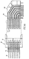
- Fig. 1A is a side view of an exemplary conductive (ground) plate 10 having a series of extruded or drawn barrels 15 and a series of pins or lances 20.
- the conductive plate 10 preferably comprises an electrically conductive metal.
- the conductive plate 10 connects to a ground plane (not shown).
- Each of the drawn barrels 15 is elongated and tubular, and preferably possesses a generally cylindrical configuration.
- the drawn barrels 15 are hollow throughout their length and are positioned so that the longitudinal axes of all the drawn barrels 15 are parallel to one another. Although the drawn barrels 15 are illustrated as being cylindrical, other shapes are possible.
- the top surfaces of all of the drawn barrels 15 are disposed in a common plane.
- the lower end surfaces of all of the drawn barrels 15 are coplanar.
- the drawn barrels 15 are disposed in aligned rows and columns so that the center of each drawn barrel 15 in a given row (column) lies along a straight line with respect to a drawn barrel 15 in the immediately adjacent rows (columns).
- Each of the pins 20 are preferably essentially flat lanced pins (hereinafter referred to as lances) and are positioned so that the longitudinal axes of all the lances 20 are parallel to one another.
- the top surfaces of all of the lances 20 are disposed in a common plane.
- the lower end surfaces of all of the lances 20 are coplanar.
- the lances 20 are disposed in aligned rows and columns so that the center of each lance 20 in a given row (column) lies along a straight line with respect to a lance 20 in the immediately adjacent rows (columns).
- the preferable pitch of drawn barrels and lances is 2mm, and preferably a lance is interposed between two adjacently located barrels.
- Each of the drawn barrels 15 receive a pin, preferably a signal pin, and each of the lances 20 act as ground connection and are formed of the conductive plate 10 between the drawn barrels 15.
- Figs. 2A and 2B show the exemplary structure of Figs. 1A and 1B with an overmolding of a polymer.
- Figs. 2A and 2B contain elements similar to those described above with respect to Figs. 1A and 1B. These elements are labeled identically and their description is omitted for brevity.
- a polymer overmold 30 is disposed over portions of the conductive plate 10 and on the interior surface (preferably, circumference) of the drawn barrels 15.
- the polymer overmold 30 effects a coaxial style construction.
- the overmold 30 acts as an insulator element and electrically and mechanically separates the drawn barrels 15 from the lances 20 (i.e., the signal pins from the ground connection).
- the lances 20 remain in electrical contact with ground connection portions 35 of the conductive plate 10 on the surface of the conductive plate 10 between the drawn barrels 15.
- the inner circumference of the barrels 15 have the polymer overmold 30.
- a hollow pinhole 40 remains in the center of each of the drawn barrels 15 to receive a signal pin 50 in each pinhole 40, as shown in Figs. 3A and 3B.
- Each signal pin 50 is generally circular and installed in the pinhole 40 in each barrel 15.
- the polymer 30 provides electrical and mechanical insulation between the signal pin 50 and the ground connection portions 35.
- the signal pin 50 acts as a contact receiving member.
- the structure in Figs. 3A and 3B effect a header connector 60.
- the header connector 60 can be mounted on or connected to a first printed card, called a motherboard.
- the header connector 60 can be formed by insert molding in which a housing, acting as the header connector 60, and insulator elements having the pinholes are formed of a continuous molded material, such as a polymer.
- Fig. 4A is a sectional side elevational view of an embodiment of a high speed transmission connector, with the parts separated, according to the present invention.
- a straight type of header connector 60 is comprised of a header housing 33 and pins (male contacts) 50 for a signal transmission line and pins (male contacts) 20 for a ground line. These pins 50 and 20 are alternately arranged in a plurality of rows on the header housing 33 of the associated connector 60.
- the pins are preferably stamped and formed with the preferred material being phosphor bronze or beryllium copper.
- a right angle type of socket connector 100 is comprised of a receptacle housing 102, ground receptacle contacts 110 for a ground line, and signal receptacle contacts 115 for a signal transmission line.
- a plurality of rows of the contacts 110 and 115 are regularly arranged so as to correspond to those of the header connector 60.
- the housing 102 is preferably molded, using a plastic material such as a high temperature thermoplastic.
- the contacts are preferably stamped and formed of beryllium copper or phosphor bronze.
- the socket connector 100 can be connected to or mounted on a second printed card, called a daughterboard.
- a daughterboard By bringing the header connector 60 and the socket connector 100 together, the header connector 60 is mated with the socket connector 100, thereby connecting the motherboard to the daughterboard.
- the ground contact 110 mates with the ground connection 35 and the signal contact 115 mates with the signal pin 50.
- the raised surface ground connection 35 engages the ground receptacle contact 110
- the signal pin 50 engages the signal receptacle contact 115 to provide electrical isolation to other signal contacts that are within the connector module in the contact engagement area.
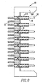
- a plurality of the connectors of Fig. 4A can be arranged in a housing 1 in an array pattern, as shown in Fig. 4B.
- the housing 1 is preferably formed of an electrically insulating material and comprises a header housing 3 having an array of header connectors 60, and a socket housing 5 having an array of socket connectors 100.
- Fig. 4C shows the header connector 60 in contact, but prior to full engagement, with the contacts 110 and 115 of a socket connector.
- the ground receptacle contacts are preferably a plurality of dual cantilever beam ground contacts 110 and are positioned for mating with respective ground connection portions 35 of the conductive plate.
- the signal receptacle contacts are preferably a plurality of single cantilever beam signal contacts 115 and are positioned for mating with respective signal pins 50.
- a top view of this arrangement is shown in Fig. 4D.
- Figs. 5A and 5B are similar to Figs. 4C and 4D, and include a ground plane 210 mated to the header connector 60.
- Fig. 5C is a side view of an exemplary mating interface in accordance with the present invention in which the header connector 60 is matingly engaged with the socket connector.
- the cantilever beam contacts 110 (only one of each pair is shown) of the socket connector housing 102 contact ground connections 35 which are electrically coupled with lances (ground pins) 20.
- the cantilever beam signal contacts 115 contact signal pins 50.
- Figs. 6A through 6C show another exemplary connector in accordance with the present invention.
- Figs. 6A through 6C are similar to Figs. 5A through 5C, but tuning fork style signal contacts 120 are used as signal contacts instead of cantilever beam signal contacts 115.
- Figs. 7A through 7C show another exemplary connector in accordance with the present invention.
- Figs. 7A through 7C are similar to Figs. 6A through 6C, but the tuning fork style signal contacts 120 are rotated approximately 45 degrees in a clockwise or counterclockwise direction around the signal pins 50. This rotation increases the distance between signals and brings the signals closer to the ground plane, for increased signal integrity.
- Fig. 8 is a side view of an exemplary perforated plate and individual cylinders 310, preferably metal, in accordance with the present invention.
- Fig. 8 is similar to Fig. 3A except an extruded conductive plate is not used. Instead, a perforated plate 300 is used.
- Individual cylinders 310 are formed to receive the signal pins 50.
- the cylinders 310 can be drawn, rolled, or cut.
- a polymer overmold 30 is inserted in the cylinders 310 to separate the signal pins 50 from the ground connections 35.
- the embodiment of Fig. 8 is used to extend the ground bus all the way through the header connector to a backplane.
- the cylinders are attached to the plate by soldering, welding, press-fitting, or swaging.
- the socket connector of the illustrated embodiments is provided with right angle portion, the present invention is not limited thereto.
- the present invention can be applied to a socket connector (not shown) having a straight type ground contact and a straight type signal contact, without a right angle portion.
Description
- The present invention relates in general to electrical connectors. More particularly, the present invention relates to a connector assembly for use in connection with circuit boards. Even more particularly, the present invention relates to a connector assembly for providing electrical interconnection between two printed circuit boards or the like.
- In electronic equipment, there is a need for electrical connectors providing connections in signal paths, and often the signal paths are so closely spaced that difficulties arise from interference between signals being transmitted along adjacent paths.
- As a general matter, many types of connectors are not well suited for preventing electrical interference or crosstalk between adjacent signal connections. As the signal speed becomes higher and the signal connections located closer to one another, this interference or crosstalk becomes even more problematic. This concern with electrical interference or crosstalk also arises in other contexts such as, for example, when one printed circuit board (e.g., a daughterboard) is mounted on another printed circuit board (e.g., a motherboard) and in the case of fast clock speed or high speed data transmission.
- Thus, in high speed backplane applications, low crosstalk between signal currents passing through the connector is desirable. Additionally, maximizing signal density is also desirable. Low crosstalk allows the electronics to switch at higher frequencies without problems. High density increases the number of circuits that can be routed through the connector.
- The
document EP 0 692 845 A1 discloses a shielded coaxial connector which comprises a parallelepiped conducting housing of two hollow parts. Said housing is riveted to a separate conducting ground plate from which mass contacts protrude. - From the
document EP 0 311 041 A2 a connector for the high-speed transmission of signals is known. It comprises a flat conductive member, having first arms at one side of the member, which are cut and raised to contact ground pins and second arms at the other side of the member, which are cut and raised to contact coaxial pins of a coaxial cable. - Although the art of connector assemblies is well developed, there remain some problems inherent in this technology, particularly electrical interference and crosstalk between adjacent signal connections. Therefore, a need exists for a connector assembly that is well suited for preventing interference or crosstalk between adjacent signal connections.
- The present invention is directed to a connector comprising a conductive ground plate having first and second faces, a plurality of first protrusions protruding from the first face, and a plurality of second protrusions protruding from the second face, the second protrusions being substantially cylindrical, hollow and forming respective raised ground surfaces; a plurality of insulator elements, each being disposed around the inner surface of the second protrusions, and having a pinhole; a plurality of signal pins, one signal pin extending through each of the pinholes in the insulator elements and through the conductive ground plate and separated from the conductive ground plate by the insulator elements, and one of the raised ground surfaces surrounding respective insulator elements and signal pins.
- In the present invention, the second protrusions are drawn. Each of the second protrusions have a top surface and a lower surface, the top surfaces being disposed in a first common plane, and the lower surfaces being disposed in a second common plane.
- In a further embodiment within the scope of the present invention, a connector system for mounting to a circuit substrate comprises a housing and a connector module supported by the housing. The connector module includes a conductive ground plate having first and second faces, a plurality of first protrusions protruding from the first face, and a plurality of second protrusions protruding from the second face, the second protrusions being hollow and forming a raised ground surface; a plurality of insulator elements, each respective insulator element having a pinhole disposed around the inner surface of each of the second protrusions; a plurality of signal pins, one of the signal pins extending through respective ones of the pinholes in the insulator elements and through the conductive ground plate and separated from the conductive ground plate by the insulator elements, and one of the raised ground surfaces surrounding respective insulator elements and signal pins; and a plurality of socket connectors, each having a plurality of signal receptacle contacts and a plurality of ground receptacle contacts, so that, in mated condition, each respective signal contact mechanically connects and electrically contacts with each respective signal pin, and each of the ground contacts mechanically connects and electrically contacts with respective raised ground surfaces.
- Another embodiment within the scope of this invention includes each socket connector comprising a receptacle housing, and each socket connector is a right angle type of socket connector, each signal receptacle contact is a single cantilevered signal receptacle contact, and each ground receptacle contact is a dual cantilevered ground receptacle contact.
- Another embodiment within the scope of this invention includes each socket connector comprising a receptacle housing, and each socket connector is a right angle type of socket connector, each signal receptacle contact is a tuning fork style signal contact, and each ground receptacle contact is a dual cantilevered ground receptacle contact.
- The foregoing and other aspects of the present invention will become apparent from the following detailed description of the invention when considered in conjunction with the accompanying drawing.
-
- Fig. 1A is a side view of an exemplary conductive plate with an array of drawn barrels and a lanced section in accordance with the present invention;
- Fig. 1B is a top view of the array of Fig. 1A;
- Fig. 2A is a side view of an exemplary plate overmolded with a polymer in accordance with the present invention;
- Fig. 2B is a top view of the plate of Fig. 2A;
- Fig. 3A is a side view of an exemplary plate with installed pins;
- Fig. 3B is a top view of the plate of Fig. 3A;
- Fig. 4A is a sectional side elevational view of an embodiment of a high speed transmission connector, with the parts separated, according to the present invention;
- Fig. 4B is a perspective view of an array of a plurality of the connectors of Fig. 4A arranged in a housing, with the parts separated;
- Fig. 4C is a side view of an exemplary plate having dual cantilever beam ground contacts and single cantilever beam signal contacts;
- Fig. 4D is a top view of the plate of Fig. 4C;
- Fig 5A is a side view of an exemplary a ground plane in accordance with the present invention;
- Fig. 5B is a top view showing of the ground plane of Fig. 5A;
- Fig. 5C is a side view of an exemplary mating interface in accordance with the present invention;
- Fig. 6A is a side view of an exemplary ground plane mated to a coaxial header with tuning fork style signal contacts in accordance with the present invention;
- Fig. 6B is a top view of the ground plane and tuning fork style contacts of Fig. 6A;
- Fig. 6C is a side view of a further exemplary mating interface in accordance with the present invention;
- Fig. 7A is a side view of an exemplary ground plane having a tuning fork interface that is rotated 45 degrees;
- Fig. 7B is a top view of the exemplary ground plane of Fig. 7A;
- Fig. 7C is a side view of a further exemplary mating interface in accordance with the present invention; and
- Fig. 8 is a side view of an exemplary perforated plate and individual drawn cylinders in accordance with the present invention.
-
- The present invention is directed to a coaxial style backplane header connector and socket receptacle connector. The present invention uses a coax style extruded plate as a central element. A mating connector employs a strip line construction for reduced crosstalk and controlled impedance.
- Fig. 1A is a side view of an exemplary conductive (ground)
plate 10 having a series of extruded or drawnbarrels 15 and a series of pins or lances 20. Theconductive plate 10 preferably comprises an electrically conductive metal. Theconductive plate 10 connects to a ground plane (not shown). Each of the drawn barrels 15 is elongated and tubular, and preferably possesses a generally cylindrical configuration. The drawn barrels 15 are hollow throughout their length and are positioned so that the longitudinal axes of all the drawn barrels 15 are parallel to one another. Although the drawn barrels 15 are illustrated as being cylindrical, other shapes are possible. - Preferably, the top surfaces of all of the drawn barrels 15 are disposed in a common plane. Likewise, the lower end surfaces of all of the drawn barrels 15 are coplanar. Also, as illustrated in Fig. 1B, the drawn barrels 15 are disposed in aligned rows and columns so that the center of each drawn
barrel 15 in a given row (column) lies along a straight line with respect to a drawnbarrel 15 in the immediately adjacent rows (columns). - Each of the
pins 20 are preferably essentially flat lanced pins (hereinafter referred to as lances) and are positioned so that the longitudinal axes of all thelances 20 are parallel to one another. Preferably, the top surfaces of all of thelances 20 are disposed in a common plane. Likewise, the lower end surfaces of all of thelances 20 are coplanar. Also, thelances 20 are disposed in aligned rows and columns so that the center of eachlance 20 in a given row (column) lies along a straight line with respect to alance 20 in the immediately adjacent rows (columns). - The preferable pitch of drawn barrels and lances is 2mm, and preferably a lance is interposed between two adjacently located barrels.
- Each of the drawn barrels 15 receive a pin, preferably a signal pin, and each of the
lances 20 act as ground connection and are formed of theconductive plate 10 between the drawn barrels 15. - Figs. 2A and 2B show the exemplary structure of Figs. 1A and 1B with an overmolding of a polymer. Figs. 2A and 2B contain elements similar to those described above with respect to Figs. 1A and 1B. These elements are labeled identically and their description is omitted for brevity.
- A
polymer overmold 30 is disposed over portions of theconductive plate 10 and on the interior surface (preferably, circumference) of the drawn barrels 15. Thepolymer overmold 30 effects a coaxial style construction. Theovermold 30 acts as an insulator element and electrically and mechanically separates the drawn barrels 15 from the lances 20 (i.e., the signal pins from the ground connection). Thelances 20 remain in electrical contact withground connection portions 35 of theconductive plate 10 on the surface of theconductive plate 10 between the drawn barrels 15. - As shown in Fig. 2B, the inner circumference of the
barrels 15 have thepolymer overmold 30. A hollow pinhole 40 remains in the center of each of the drawn barrels 15 to receive asignal pin 50 in each pinhole 40, as shown in Figs. 3A and 3B. Eachsignal pin 50 is generally circular and installed in the pinhole 40 in eachbarrel 15. Thepolymer 30 provides electrical and mechanical insulation between thesignal pin 50 and theground connection portions 35. Thesignal pin 50 acts as a contact receiving member. The structure in Figs. 3A and 3B effect aheader connector 60. Theheader connector 60 can be mounted on or connected to a first printed card, called a motherboard. Theheader connector 60 can be formed by insert molding in which a housing, acting as theheader connector 60, and insulator elements having the pinholes are formed of a continuous molded material, such as a polymer. - Fig. 4A is a sectional side elevational view of an embodiment of a high speed transmission connector, with the parts separated, according to the present invention. A straight type of
header connector 60 is comprised of aheader housing 33 and pins (male contacts) 50 for a signal transmission line and pins (male contacts) 20 for a ground line. Thesepins header housing 33 of the associatedconnector 60. The pins are preferably stamped and formed with the preferred material being phosphor bronze or beryllium copper. - A right angle type of
socket connector 100 is comprised of areceptacle housing 102,ground receptacle contacts 110 for a ground line, and signalreceptacle contacts 115 for a signal transmission line. A plurality of rows of thecontacts header connector 60. Thehousing 102 is preferably molded, using a plastic material such as a high temperature thermoplastic. The contacts are preferably stamped and formed of beryllium copper or phosphor bronze. - The
socket connector 100 can be connected to or mounted on a second printed card, called a daughterboard. By bringing theheader connector 60 and thesocket connector 100 together, theheader connector 60 is mated with thesocket connector 100, thereby connecting the motherboard to the daughterboard. When mated, theground contact 110 mates with theground connection 35 and thesignal contact 115 mates with thesignal pin 50. In other words, the raisedsurface ground connection 35 engages theground receptacle contact 110, and thesignal pin 50 engages thesignal receptacle contact 115 to provide electrical isolation to other signal contacts that are within the connector module in the contact engagement area. - A plurality of the connectors of Fig. 4A can be arranged in a housing 1 in an array pattern, as shown in Fig. 4B. The housing 1 is preferably formed of an electrically insulating material and comprises a
header housing 3 having an array ofheader connectors 60, and a socket housing 5 having an array ofsocket connectors 100. - Fig. 4C shows the
header connector 60 in contact, but prior to full engagement, with thecontacts beam ground contacts 110 and are positioned for mating with respectiveground connection portions 35 of the conductive plate. The signal receptacle contacts are preferably a plurality of single cantileverbeam signal contacts 115 and are positioned for mating with respective signal pins 50. A top view of this arrangement is shown in Fig. 4D. - Figs. 5A and 5B are similar to Figs. 4C and 4D, and include a
ground plane 210 mated to theheader connector 60. Fig. 5C is a side view of an exemplary mating interface in accordance with the present invention in which theheader connector 60 is matingly engaged with the socket connector. The cantilever beam contacts 110 (only one of each pair is shown) of thesocket connector housing 102contact ground connections 35 which are electrically coupled with lances (ground pins) 20. The cantileverbeam signal contacts 115 contact signal pins 50. By bringing theheader connector 60 and the socket connector together, theheader connector 60 is mated with the socket connector, thereby connecting the motherboard to the daughterboard. - Figs. 6A through 6C show another exemplary connector in accordance with the present invention. Figs. 6A through 6C are similar to Figs. 5A through 5C, but tuning fork
style signal contacts 120 are used as signal contacts instead of cantileverbeam signal contacts 115. - Figs. 7A through 7C show another exemplary connector in accordance with the present invention. Figs. 7A through 7C are similar to Figs. 6A through 6C, but the tuning fork
style signal contacts 120 are rotated approximately 45 degrees in a clockwise or counterclockwise direction around the signal pins 50. This rotation increases the distance between signals and brings the signals closer to the ground plane, for increased signal integrity. - Fig. 8 is a side view of an exemplary perforated plate and
individual cylinders 310, preferably metal, in accordance with the present invention. Fig. 8 is similar to Fig. 3A except an extruded conductive plate is not used. Instead, aperforated plate 300 is used.Individual cylinders 310 are formed to receive the signal pins 50. Thecylinders 310 can be drawn, rolled, or cut. Apolymer overmold 30 is inserted in thecylinders 310 to separate the signal pins 50 from theground connections 35. The embodiment of Fig. 8 is used to extend the ground bus all the way through the header connector to a backplane. The cylinders are attached to the plate by soldering, welding, press-fitting, or swaging. - It should be noted that although the socket connector of the illustrated embodiments is provided with right angle portion, the present invention is not limited thereto. For example, the present invention can be applied to a socket connector (not shown) having a straight type ground contact and a straight type signal contact, without a right angle portion.
- Although illustrated and described herein with reference to certain specific embodiments, the present invention is nevertheless not intended to be limited to the details shown. Rather, various modifications may be made in the details within the scope and range of equivalents of the claims and without departing from the invention.
Claims (10)
- A connector comprising:a. a conductive ground plate (10) having first and second faces, and a plurality of first protrusions (20) protruding from said first face; andb. a plurality of second protrusions (15) protruding from said second face, said second protrusions (15) being substantially cylindrical, hollow and forming respective raised ground surfaces (35);c. a plurality of insulator elements (30), each being disposed around the inner surface of said second protrusions (15), and having a pinhole (40); andd. a plurality of signal pins (50), one signal pin (50) extending through each of said pinholes (40) in said insulator elements (30) and through said conductive ground plate (10) and separated from said conductive ground plate (10) by said insulator elements (30), and one of said raised ground surfaces (15) surrounding respective insulator elements (30) and signal pins (50).
- The connector of claim 1, wherein said second protrusions (15) are drawn.
- The connector of claim 1, wherein each of said second protrusions (15) have a top surface and a lower surface, said top surfaces being disposed in a first common plane, and said lower surfaces being disposed in a second common plane; or wherein said first protrusions (20) are substantially flat lanced pins.
- The connector of claim 1, wherein the longitudinal axes of each of said first protrusions (20) are parallel to one another; or wherein each of said first protrusions (20) have a top surface and a lower surface, said top surfaces being coplanar, and said lower surfaces being coplanar.
- The connector of claim 1, wherein each respective first protrusion (20) is interposed between two adjacent second protrusions (15); or wherein the conductive ground plate (10) comprises an electrically conductive metal; or wherein each of said insulator elements (30) is a polymer.
- The connector of claim 1, further comprising:a. a housing (1);b. a plurality of socket connectors (100), each having a plurality of signal receptacle contacts (115); and a plurality of ground receptacle contacts (110), so that,c. in mated condition, each respective signal contact (115) mechanically connects and electrically contacts with each respective signal pin (50), and each of said ground contacts (115) mechanically connects and electrically contacts with respective raised ground surfaces (15).
- The connector of claim 6, wherein each of said socket connectors (100) further comprises a receptacle housing, and
therein each said socket connector (100) is a right angle type of socket connector, each said signal receptacle contact (115) is a single cantilevered signal receptacle contact, and each said ground receptacle contact (110) is a dual cantilevered ground receptacle contact. - The connector of claim 7, wherein each of said socket connectors (100) further comprises a receptacle housing, and
wherein each said socket connector (100) is a right angle type of socket connector, each said signal receptacle contact is a tuning fork style signal contact (120), and each said ground receptacle contact (110) is a dual cantilevered ground receptacle contact; and in particular wherein each said tuning fork style signal contact (120) is rotated 45 degrees around a respective signal pin. - The connector of claim 1 or 6, wherein said conductive ground plate (10) is extruded; or wherein said conductive ground plate (10) is perforated.
- The connector of claim 6, wherein said housing (1) and insulator elements (30) having said pinholes are formed of a continuous molded material.
Applications Claiming Priority (2)
| Application Number | Priority Date | Filing Date | Title |
|---|---|---|---|
| US08/942,082 US6056559A (en) | 1997-10-01 | 1997-10-01 | Punched sheet coax header |
| US942082 | 1997-10-01 |
Publications (3)
| Publication Number | Publication Date |
|---|---|
| EP0907219A2 EP0907219A2 (en) | 1999-04-07 |
| EP0907219A3 EP0907219A3 (en) | 2000-05-10 |
| EP0907219B1 true EP0907219B1 (en) | 2004-07-14 |
Family
ID=25477549
Family Applications (1)
| Application Number | Title | Priority Date | Filing Date |
|---|---|---|---|
| EP98118459A Expired - Lifetime EP0907219B1 (en) | 1997-10-01 | 1998-09-30 | Punched sheet coax header |
Country Status (6)
| Country | Link |
|---|---|
| US (1) | US6056559A (en) |
| EP (1) | EP0907219B1 (en) |
| JP (1) | JPH11162579A (en) |
| CN (1) | CN1115748C (en) |
| DE (1) | DE69825005T2 (en) |
| TW (1) | TW390536U (en) |
Families Citing this family (16)
| Publication number | Priority date | Publication date | Assignee | Title |
|---|---|---|---|---|
| US6227882B1 (en) * | 1997-10-01 | 2001-05-08 | Berg Technology, Inc. | Connector for electrical isolation in a condensed area |
| US6364710B1 (en) * | 2000-03-29 | 2002-04-02 | Berg Technology, Inc. | Electrical connector with grounding system |
| JP4434422B2 (en) * | 2000-04-04 | 2010-03-17 | Necトーキン株式会社 | High frequency current suppression type connector |
| US6787116B2 (en) | 2001-05-02 | 2004-09-07 | Aquatherm Industries, Inc. | Overmolding insert for heat exchanger, process for manufacturing a heat exchanger, and heat exchanger produced thereby |
| US6905367B2 (en) * | 2002-07-16 | 2005-06-14 | Silicon Bandwidth, Inc. | Modular coaxial electrical interconnect system having a modular frame and electrically shielded signal paths and a method of making the same |
| MXPA06012162A (en) * | 2004-04-27 | 2007-03-30 | Galapagos Nv | Methods, agents, and compound screening assays for inducing differentiation of undifferentiated mammalian cells into osteoblasts. |
| US7371117B2 (en) * | 2004-09-30 | 2008-05-13 | Amphenol Corporation | High speed, high density electrical connector |
| US6986682B1 (en) * | 2005-05-11 | 2006-01-17 | Myoungsoo Jeon | High speed connector assembly with laterally displaceable head portion |
| US7850489B1 (en) | 2009-08-10 | 2010-12-14 | 3M Innovative Properties Company | Electrical connector system |
| US7997933B2 (en) | 2009-08-10 | 2011-08-16 | 3M Innovative Properties Company | Electrical connector system |
| US7927144B2 (en) * | 2009-08-10 | 2011-04-19 | 3M Innovative Properties Company | Electrical connector with interlocking plates |
| US7909646B2 (en) * | 2009-08-10 | 2011-03-22 | 3M Innovative Properties Company | Electrical carrier assembly and system of electrical carrier assemblies |
| US9099820B2 (en) * | 2013-09-18 | 2015-08-04 | Delphi Technologies, Inc. | Electronics module with a side entry connection |
| KR102214509B1 (en) | 2014-09-01 | 2021-02-09 | 삼성전자 주식회사 | Test socket for semiconductor devices and test equipment comprising the same |
| CN110265838B (en) * | 2019-07-05 | 2024-03-22 | 上海航天科工电器研究院有限公司 | Radio frequency coaxial connector |
| DE102021205038A1 (en) * | 2021-05-18 | 2022-11-24 | Robert Bosch Gesellschaft mit beschränkter Haftung | Connector element and electronic module |
Family Cites Families (22)
| Publication number | Priority date | Publication date | Assignee | Title |
|---|---|---|---|---|
| US3435387A (en) * | 1965-09-01 | 1969-03-25 | Allen Bradley Co | Solderless mounting filter connection |
| US3587028A (en) * | 1969-04-28 | 1971-06-22 | Ibm | Coaxial connector guide and grounding structure |
| US4020430A (en) * | 1975-04-28 | 1977-04-26 | Amp Incorporated | Filtered connector assembly with composite ground plane |
| US4046445A (en) * | 1976-08-23 | 1977-09-06 | International Telephone And Telegraph Corporation | Spring bushing for conductive back-plane connection |
| US4296990A (en) * | 1980-02-22 | 1981-10-27 | Virginia Panel Corporation | Electrical connector having insulated locking shell for use on panel having metal ground plane |
| US4606598A (en) * | 1985-05-02 | 1986-08-19 | Itt Corporation | Grounding plate connector |
| US4749355A (en) * | 1987-04-30 | 1988-06-07 | Amphenol Corporation | Coaxial contact for termination to printed circuit boards and the like |
| JPH0821450B2 (en) * | 1987-10-05 | 1996-03-04 | 日本電気株式会社 | High-speed signal connector |
| US4867690A (en) * | 1988-06-17 | 1989-09-19 | Amp Incorporated | Electrical connector system |
| JP2739608B2 (en) * | 1990-11-15 | 1998-04-15 | 日本エー・エム・ピー株式会社 | Multi-contact type connector for signal transmission |
| US5169343A (en) * | 1990-11-29 | 1992-12-08 | E. I. Du Pont De Nemours And Company | Coax connector module |
| US5198958A (en) * | 1991-06-03 | 1993-03-30 | Amphenol Corporation | Transient suppression component |
| US5194020A (en) * | 1991-06-17 | 1993-03-16 | W. L. Gore & Associates, Inc. | High-density coaxial interconnect system |
| EP0608220B1 (en) * | 1991-10-17 | 1996-02-28 | Itt Industries, Inc. | Connector with interchangeable contacts |
| FR2685553A1 (en) * | 1991-12-18 | 1993-06-25 | Radiall Sa | COAXIAL CONNECTOR ELEMENT ELBOW FIXED TO A PRINTED BOARD. |
| DE9210810U1 (en) * | 1992-08-12 | 1992-10-15 | Siemens Ag, 8000 Muenchen, De | |
| FR2702095B1 (en) * | 1993-02-26 | 1995-04-14 | Radiall Sa | Angled coaxial connector element capable of being fixed to a printed circuit board. |
| JPH07122335A (en) * | 1993-10-20 | 1995-05-12 | Minnesota Mining & Mfg Co <3M> | Connector for high-speed transmission |
| JP2901878B2 (en) * | 1994-07-15 | 1999-06-07 | オリンパス光学工業株式会社 | Wire connector |
| US5562462A (en) * | 1994-07-19 | 1996-10-08 | Matsuba; Stanley | Reduced crosstalk and shielded adapter for mounting an integrated chip package on a circuit board like member |
| DE4438872C1 (en) * | 1994-11-03 | 1995-12-07 | Harting Elektronik Gmbh | Coaxial angle connector for PCB |
| US5795191A (en) * | 1996-09-11 | 1998-08-18 | Preputnick; George | Connector assembly with shielded modules and method of making same |
-
1997
- 1997-10-01 US US08/942,082 patent/US6056559A/en not_active Expired - Lifetime
-
1998
- 1998-09-11 TW TW087215020U patent/TW390536U/en not_active IP Right Cessation
- 1998-09-30 EP EP98118459A patent/EP0907219B1/en not_active Expired - Lifetime
- 1998-09-30 JP JP10276276A patent/JPH11162579A/en active Pending
- 1998-09-30 CN CN98120852A patent/CN1115748C/en not_active Expired - Fee Related
- 1998-09-30 DE DE69825005T patent/DE69825005T2/en not_active Expired - Fee Related
Also Published As
| Publication number | Publication date |
|---|---|
| CN1115748C (en) | 2003-07-23 |
| JPH11162579A (en) | 1999-06-18 |
| EP0907219A3 (en) | 2000-05-10 |
| US6056559A (en) | 2000-05-02 |
| EP0907219A2 (en) | 1999-04-07 |
| DE69825005T2 (en) | 2005-07-21 |
| CN1213875A (en) | 1999-04-14 |
| TW390536U (en) | 2000-05-11 |
| DE69825005D1 (en) | 2004-08-19 |
Similar Documents
| Publication | Publication Date | Title |
|---|---|---|
| EP0446980B2 (en) | Connector assembly for printed circuit boards | |
| US6042394A (en) | Right-angle connector | |
| EP0632933B1 (en) | A miniaturized high-density coaxial connector system with staggered grouper modules | |
| US4992052A (en) | Modular connector system with high contact element density | |
| US5197893A (en) | Connector assembly for printed circuit boards | |
| US6712646B2 (en) | High-speed transmission connector with a ground structure having an improved shielding function | |
| US5620340A (en) | Connector with improved shielding | |
| EP0620616B1 (en) | Connector for coaxial and/or twinaxial cables | |
| US6551140B2 (en) | Electrical connector having differential pair terminals with equal length | |
| EP2250707B1 (en) | High-speed backplane connector | |
| US7179127B2 (en) | Connector minimized in cross-talk and electrical interference | |
| US6120306A (en) | Cast coax header/socket connector system | |
| US7044748B2 (en) | Electrical device for interconnecting two printed circuit boards at a large distance | |
| EP0907219B1 (en) | Punched sheet coax header | |
| US20100009571A1 (en) | Carrier assembly and system configured to commonly ground a header | |
| US6837741B2 (en) | Connector and cable positioning member of connector | |
| US6592407B2 (en) | High-speed card edge connector | |
| US20220173550A1 (en) | Integrally shielded cable connector | |
| US6918774B2 (en) | Electrical connector having long circuit boards | |
| EP0677215B1 (en) | A connector with improved shielding | |
| US6443740B1 (en) | Connector system | |
| EP0393251B1 (en) | Modular connector system with high contact element density surface mounted connectors | |
| US5013261A (en) | Device for connecting a coaxial cable | |
| CA2089461C (en) | Circuit board connector | |
| KR100513179B1 (en) | Punched sheet coax header |
Legal Events
| Date | Code | Title | Description |
|---|---|---|---|
| PUAI | Public reference made under article 153(3) epc to a published international application that has entered the european phase |
Free format text: ORIGINAL CODE: 0009012 |
|
| AK | Designated contracting states |
Kind code of ref document: A2 Designated state(s): CH DE FR GB IT LI |
|
| AX | Request for extension of the european patent |
Free format text: AL;LT;LV;MK;RO;SI |
|
| RIC1 | Information provided on ipc code assigned before grant |
Free format text: 7H 01R 9/05 A, 7H 01R 23/68 B, 7H 01R 17/12 B |
|
| PUAL | Search report despatched |
Free format text: ORIGINAL CODE: 0009013 |
|
| RIC1 | Information provided on ipc code assigned before grant |
Free format text: 7H 01R 9/05 A, 7H 01R 23/68 B, 7H 01R 17/12 B, 7H 01R 23/70 B |
|
| AK | Designated contracting states |
Kind code of ref document: A3 Designated state(s): AT BE CH CY DE DK ES FI FR GB GR IE IT LI LU MC NL PT SE |
|
| AX | Request for extension of the european patent |
Free format text: AL;LT;LV;MK;RO;SI |
|
| 17P | Request for examination filed |
Effective date: 20000927 |
|
| AKX | Designation fees paid |
Free format text: CH DE FR GB IT LI |
|
| 17Q | First examination report despatched |
Effective date: 20010926 |
|
| GRAP | Despatch of communication of intention to grant a patent |
Free format text: ORIGINAL CODE: EPIDOSNIGR1 |
|
| GRAS | Grant fee paid |
Free format text: ORIGINAL CODE: EPIDOSNIGR3 |
|
| RAP1 | Party data changed (applicant data changed or rights of an application transferred) |
Owner name: FCI |
|
| GRAA | (expected) grant |
Free format text: ORIGINAL CODE: 0009210 |
|
| RIC1 | Information provided on ipc code assigned before grant |
Ipc: 7H 01R 12/18 B Ipc: 7H 01R 12/16 B Ipc: 7H 01R 13/646 B Ipc: 7H 01R 9/05 A |
|
| RIC1 | Information provided on ipc code assigned before grant |
Ipc: 7H 01R 9/05 A |
|
| AK | Designated contracting states |
Kind code of ref document: B1 Designated state(s): CH DE FR GB IT LI |
|
| PG25 | Lapsed in a contracting state [announced via postgrant information from national office to epo] |
Ref country code: LI Free format text: LAPSE BECAUSE OF FAILURE TO SUBMIT A TRANSLATION OF THE DESCRIPTION OR TO PAY THE FEE WITHIN THE PRESCRIBED TIME-LIMIT Effective date: 20040714 Ref country code: CH Free format text: LAPSE BECAUSE OF FAILURE TO SUBMIT A TRANSLATION OF THE DESCRIPTION OR TO PAY THE FEE WITHIN THE PRESCRIBED TIME-LIMIT Effective date: 20040714 |
|
| REG | Reference to a national code |
Ref country code: GB Ref legal event code: FG4D |
|
| REG | Reference to a national code |
Ref country code: CH Ref legal event code: EP |
|
| REF | Corresponds to: |
Ref document number: 69825005 Country of ref document: DE Date of ref document: 20040819 Kind code of ref document: P |
|
| REG | Reference to a national code |
Ref country code: CH Ref legal event code: PL |
|
| ET | Fr: translation filed | ||
| PLBE | No opposition filed within time limit |
Free format text: ORIGINAL CODE: 0009261 |
|
| STAA | Information on the status of an ep patent application or granted ep patent |
Free format text: STATUS: NO OPPOSITION FILED WITHIN TIME LIMIT |
|
| 26N | No opposition filed |
Effective date: 20050415 |
|
| PGFP | Annual fee paid to national office [announced via postgrant information from national office to epo] |
Ref country code: GB Payment date: 20070809 Year of fee payment: 10 |
|
| PGFP | Annual fee paid to national office [announced via postgrant information from national office to epo] |
Ref country code: IT Payment date: 20070913 Year of fee payment: 10 Ref country code: DE Payment date: 20070928 Year of fee payment: 10 |
|
| PGFP | Annual fee paid to national office [announced via postgrant information from national office to epo] |
Ref country code: FR Payment date: 20070904 Year of fee payment: 10 |
|
| GBPC | Gb: european patent ceased through non-payment of renewal fee |
Effective date: 20080930 |
|
| REG | Reference to a national code |
Ref country code: FR Ref legal event code: ST Effective date: 20090529 |
|
| PG25 | Lapsed in a contracting state [announced via postgrant information from national office to epo] |
Ref country code: IT Free format text: LAPSE BECAUSE OF NON-PAYMENT OF DUE FEES Effective date: 20080930 Ref country code: DE Free format text: LAPSE BECAUSE OF NON-PAYMENT OF DUE FEES Effective date: 20090401 |
|
| PG25 | Lapsed in a contracting state [announced via postgrant information from national office to epo] |
Ref country code: FR Free format text: LAPSE BECAUSE OF NON-PAYMENT OF DUE FEES Effective date: 20080930 |
|
| PG25 | Lapsed in a contracting state [announced via postgrant information from national office to epo] |
Ref country code: GB Free format text: LAPSE BECAUSE OF NON-PAYMENT OF DUE FEES Effective date: 20080930 |