EP0903852A1 - Aligning method for a multistage selective amplifier - Google Patents
Aligning method for a multistage selective amplifier Download PDFInfo
- Publication number
- EP0903852A1 EP0903852A1 EP98116588A EP98116588A EP0903852A1 EP 0903852 A1 EP0903852 A1 EP 0903852A1 EP 98116588 A EP98116588 A EP 98116588A EP 98116588 A EP98116588 A EP 98116588A EP 0903852 A1 EP0903852 A1 EP 0903852A1
- Authority
- EP
- European Patent Office
- Prior art keywords
- tuning
- frequency
- amplifier
- oscillator
- tuning voltage
- Prior art date
- Legal status (The legal status is an assumption and is not a legal conclusion. Google has not performed a legal analysis and makes no representation as to the accuracy of the status listed.)
- Granted
Links
- 238000000034 method Methods 0.000 title claims abstract description 25
- 238000004519 manufacturing process Methods 0.000 claims abstract description 7
- 230000001419 dependent effect Effects 0.000 abstract description 5
- 239000000654 additive Substances 0.000 description 7
- 230000000996 additive effect Effects 0.000 description 7
- 230000008569 process Effects 0.000 description 5
- 230000008859 change Effects 0.000 description 3
- 230000006870 function Effects 0.000 description 3
- 230000008901 benefit Effects 0.000 description 2
- 238000010586 diagram Methods 0.000 description 2
- 230000005669 field effect Effects 0.000 description 2
- 235000008694 Humulus lupulus Nutrition 0.000 description 1
- 238000004364 calculation method Methods 0.000 description 1
- 230000002542 deteriorative effect Effects 0.000 description 1
- 238000011161 development Methods 0.000 description 1
- 230000018109 developmental process Effects 0.000 description 1
- 230000000694 effects Effects 0.000 description 1
- 238000012886 linear function Methods 0.000 description 1
- 230000010355 oscillation Effects 0.000 description 1
- 230000002787 reinforcement Effects 0.000 description 1
- 230000004044 response Effects 0.000 description 1
- 230000001360 synchronised effect Effects 0.000 description 1
- 238000009966 trimming Methods 0.000 description 1
Images


Classifications
-
- H—ELECTRICITY
- H03—ELECTRONIC CIRCUITRY
- H03J—TUNING RESONANT CIRCUITS; SELECTING RESONANT CIRCUITS
- H03J1/00—Details of adjusting, driving, indicating, or mechanical control arrangements for resonant circuits in general
- H03J1/0008—Details of adjusting, driving, indicating, or mechanical control arrangements for resonant circuits in general using a central processing unit, e.g. a microprocessor
- H03J1/0033—Details of adjusting, driving, indicating, or mechanical control arrangements for resonant circuits in general using a central processing unit, e.g. a microprocessor for voltage synthesis with a D/A converter
-
- H—ELECTRICITY
- H03—ELECTRONIC CIRCUITRY
- H03J—TUNING RESONANT CIRCUITS; SELECTING RESONANT CIRCUITS
- H03J3/00—Continuous tuning
- H03J3/28—Continuous tuning of more than one resonant circuit simultaneously, the tuning frequencies of the circuits having a substantially constant difference throughout the tuning range
- H03J3/32—Arrangements for ensuring tracking with variable capacitors
Definitions
- the invention relates to a method for comparing a multi-stage selective amplifier, according to the preamble of patent claims 1 and 2.
- Tuning circuits are used to adjust the desired frequency needed to receive a particular Ensure signal that is transmitted on this frequency.
- an oscillator frequency is set on an oscillator circuit, around a fixed intermediate frequency to the desired reception frequency is shifted and fed to a mixer. From the Oscillator frequency and the pre-filtered received signal, which is also is fed to the mixer, the fixed intermediate frequency is formed.
- the mixer In front the mixer is therefore the preliminary, drain or intermediate circles, which serve as frequency filters for the reception frequency.
- the Tuning circuit serves the Tuning circuit to the fact that pre, drain or intermediate circuits on the desired reception frequency, the oscillator circuit to the one around the IF frequency offset corresponding oscillation frequency is tuned. If all circles are tuned to the target frequency, this is called Identifies synchronism with which optimal reception is guaranteed.
- EP 0 044 237 A1 describes the tuning of an electronic one Circuit, especially a television receiver, with several variable elements and the control of the oscillator frequency via a Phase locked loop known. This document mentions in particular the Matching a filter or oscillator with capacitance diodes.
- the known adjustment device contains one already at the time of Production of permanently programmed memory (PROM). It includes the Characteristic function with which the desired value can be calculated. The stored information is used to generate Control signals for electronic voting.
- the disadvantage here is that the characteristic curve is already entered into the memory during manufacture and any changes that may occur over time cannot be taken into account. Device-specific deviations cannot be included with this method either. Furthermore, it is important in this method to store as many points of the characteristic as possible in the memory, since the accuracy of this method depends on the number of characteristic points stored. Another disadvantage is the busy data traffic when changing frequencies. With each frequency change, new values must be written from the memory into the phase locked loop.
- the individual circles are compared one after the other by variation the tuning voltage assigned to the respective element.
- About one the detector connected to the output of the last circuit becomes the Adjustment of individual circles ended when the maximum of Pass curve is reached. After finishing the whole The adjustment process will switch the antenna back on instead of the oscillator switched the preliminary circuit.
- the tuning voltages determined in this way are stored digitally until a new channel is selected and the adjustment process expires again.
- the invention is therefore based on the object of demonstrating a method for comparing a multi-stage selective amplifier which sets a synchronous operation precisely, quickly and reliably without storing large amounts of data or requiring heavy traffic.
- FIG. 1 the value of the required tuning voltage, which generates the frequency required for tuning, is calculated from a mathematical relationship, the mathematical relationship being determined and stored during production or when the device is first switched on.
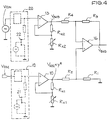
- FIG. 1 shows the principle of the tuning circuit according to the invention.
- the incoming signals S E at the pre-circuit 2 are filtered according to the reception frequency and then amplified at a first amplifier 3 .
- the signals filtered and amplified with regard to the reception frequency of the preliminary circuit 2 then pass into an intermediate circuit 4 , which again filters the signals according to the reception frequency or frequency range.
- These remaining signals are then passed on to a mixer 5 , which filters out the remaining signals exactly at a predetermined third frequency by setting an oscillator frequency on the oscillator circuit 6 which determines the desired reception frequency.
- the output signal S A is forwarded to a signal processing unit.
- the frequencies or frequency ranges of the preliminary circuit 2 and the intermediate circuit 4 must match or at least contain the reception frequency, which is determined by the oscillator frequency on the oscillator circuit 6 .
- the oscillator frequency and thus also the desired reception frequency are set via the adjustable oscillator tuning voltage.
- the oscillator circuit is controlled by a microprocessor 8 , which transmits the desired reception frequency or oscillator frequency via a phase locked loop 7 .
- the microprocessor 8 sets the corresponding oscillator tuning voltage V OSZ for the oscillator 6 in the control loop of the oscillator phase locked loop 7 .
- the phase control loop 7 is assigned the corresponding actuators for the respective tuning voltages of the associated further selection circuits.
- the preliminary and intermediate circuits 2 , 4 have the tuning voltages V VOR and V ZWI , which then set these circuits to the reception frequency defined by the oscillator circuit.
- the basis for this is an existing fixed relationship between the oscillator tuning voltage V OSZ and the tuning voltage of the pre-circuit 2 V VOR or the tuning voltage of the intermediate circuit 4 V ZWI .
- FIGS. 2A and 2B each show an example for determining the tuning curves.
- curve 1 in FIG. 2A shows the relationship between the oscillator tuning voltage V OSZ and the reception frequency f .
- V OSZ oscillator tuning voltage
- f reception frequency
- Curve 2 is obtained by multiplying curve 1 by a coefficient Y.
- Curve 3 this is the tuning curve of the preliminary or intermediate circuit, results from curve 2 and an addition with a coefficient X.
- the coefficients Y and X relevant for the respective tuning circuit can be determined once during manufacture or when the device is switched on. These values are then read into the microprocessor's memory and loaded from there into the phase locked loop.
- the coefficients are determined by first setting the oscillator to the first synchronization point A at a low reception frequency f N via the phase locked loop. Then, the corresponding receiving frequency f is fed via a signal generator and the field strength voltage in the further course of the receiver measured as known. Via the microprocessor, the associated values of all X and Y manipulated variables are varied in the sense of a maximum adjustment of this field strength voltage and the resulting values for the maxima are recorded. At the second synchronization point B at a higher reception frequency f H , this process is repeated and the values are recorded, and the respective voltages V (A) and V (B) are calculated therefrom.
- Curve 2b shows the relationship between the oscillator tuning voltage V OSZ and the reception frequency f . This relationship is logarithmic. The curves can be described by a logarithmic functional equation. Curve 2 is obtained by multiplying curve 1 by a coefficient Y as shown in FIG. 2A. Curve 3 , this is the tuning curve of the preliminary or intermediate circuit, results from curve 2 and an addition with a coefficient X.
- the type of function i.e. the basic curve of the function curve, e.g. a linear or logarithmic curve curve
- two known points on this functional curve are also sufficient to calculate all voltage values V at a given reception frequency f at least for this sub-area .
- the two coefficients Y and X are determined either once during manufacture or when the device is switched on, or again and again when the device is switched on. During the operating time of the device, these two coefficients are permanently stored in a memory.
- the respective tuning values can be calculated from the applied oscillator tuning voltage using the flow diagrams shown in FIGS. 3A and 3B .
- FIG. 3A shows the first possibility in which, starting from the oscillator tuning voltage V OSZ , the additive coefficient X is first added and then this value is multiplied by the coefficient Y.
- the second possibility shows a flow chart in which the oscillator tuning voltage V OSZ is first multiplied by another coefficient Y and only then is the other additive coefficient X added to this value.
- a circuit that realizes this possibility is shown in FIG . Both methods lead to the same result of the tuning voltage V of the preliminary circuit or intermediate circuit V VOR or V ZWI . Coefficients Y and X differ depending on the method used.
- FIG. 4 shows a tuning circuit according to the invention. This arrangement is essentially fed by two voltage sources.
- the adjustable, variable oscillator tuning voltage V OSZ is applied to the non-inverting input of a first operational amplifier 10 .
- a prescaler 19 can be installed between the oscillator tuning voltage V OSZ and the non-inverting input of the operational amplifier 10 . This alternative is shown in dashed lines in the figure.
- the prescaler 19 consists of two resistors, a field-effect transistor 21, also called an FET, and a DC voltage source.
- the DC voltage source lies between the gate and source connection of the FET 21 .
- a resistor is connected to the drain terminal, which is connected on the one hand to the oscillator tuning voltage V OSZ via another resistor and on the other hand to the non-inverting input of the first operational amplifier 10 .
- the inverting input of the first operational amplifier 10 is connected to a voltage divider, the voltage divider consists of two resistors R N1 , R X1 .
- One resistor R N1 is connected to the output of operational amplifier 10 , to the inverting input of operational amplifier 10 and to the other variable resistor R X1 , which is connected to ground on the one hand and to the inverting input of operational amplifier 10 on the other hand. This amplifies the voltage V OSZ applied to the non-inverting input.
- This amplified voltage V OSZ ⁇ Y * is applied via a resistor R 2 to the non-inverting input of a second operational amplifier 16 .
- This resistor R 2 is in turn connected to another resistor R 1 , which is also applied to the non-inverting input of the second operational amplifier 16 and to ground.
- a fixed input voltage V IN is applied to the non-inverting input of a third operational amplifier 13 .
- a prescaler 20 can be installed between the fixed input voltage V IN and the non-inverting input. This alternative is shown in dashed lines in the figure.
- the prescaler 20 consists of two resistors: a field effect transistor 22, also called an FET, and a DC voltage source.
- the DC voltage source is located between the gate and source connection of the FET 20 .
- a resistor is connected to the drain terminal, which is connected on the one hand to the fixed input voltage V IN via another resistor and on the other hand to the non-inverting input of the third operational amplifier 13 .
- the inverting input of the third operational amplifier 13 is connected to a voltage divider, as is customary in an amplifier circuit, the voltage divider consists of two resistors R X2 , R N2 .
- One resistor R N2 is connected to the output of the third operational amplifier 13 , to the inverting input of the third operational amplifier 13 and to the other variable resistor R X2 , which is connected to ground on the one hand and to the inverting input of the third operational amplifier 13 on the other hand.
- This voltage V OUT reaches the inverting input of the second operational amplifier 16 via a resistor R 4 .
- This resistor R 4 is connected to another resistor R 3 , this resistor R 3 is also connected to the inverting input of the second operational amplifier 16 and to the output of the second operational amplifier 16 .
- the voltage V END is then present at the output of the second operational amplifier 16 .
- the task of such a circuit is that the amplifier 10 amplifies the input voltage in the application example the oscillator tuning voltage V OSZ or a voltage dependent thereon by the factor Y * .
- the gain can be set linearly in a specified step size and resolution.
- the linearity can be achieved, for example, by connecting the resistor R N1 with binary graded values from the resistor R X1 .
- the variable resistor R X1 then actually consists of several resistors connected in parallel, which can be connected depending on the level of the desired resistance value.
- the gain factor Y * can be set linearly.
- the other operational amplifier 13 supplies a linearly adjustable output voltage (DA converter).
- DA converter linearly adjustable output voltage
- the predetermined X and Y coefficients can be set with this circuit.
Landscapes
- Engineering & Computer Science (AREA)
- Computer Hardware Design (AREA)
- Microelectronics & Electronic Packaging (AREA)
- Stabilization Of Oscillater, Synchronisation, Frequency Synthesizers (AREA)
- Television Receiver Circuits (AREA)
- Superheterodyne Receivers (AREA)
Abstract
Description
Die Erfindung betrifft ein Verfahren zum Abgleich eines mehrstufigen selektiven Verstärkers, gemäß dem Oberbegriff des Patentanspruches 1 und 2. The invention relates to a method for comparing a multi-stage selective amplifier, according to the preamble of patent claims 1 and 2.
Mit Tunern können verschiedene Programme oder allgemeiner Signale auf unterschiedlichen Frequenzen empfangen, verstärkt und wiedergegeben werden. Abstimmschaltungen werden zur Einstellung der gewünschten Frequenz benötigt, die den Empfang eines bestimmten Signals, welches auf dieser Frequenz übertragen wird, gewährleisten. Hierbei wird an einem Oszillatorkreis eine Oszillatorfrequenz eingestellt, die um eine feste Zwischenfrequenz zur gewünschten Empfangsfrequenz verschoben ist und einem Mischer zugeführt wird. Aus der Oszillatorfrequenz und dem vorgefilterten Empfangssignal, das gleichfalls dem Mischer zugeführt ist, wird die feste Zwischenfrequenz gebildet. Vor dem Mischer befinden sich daher die Vor-, Drain- bzw. Zwischenkreise, die als Frequenzfilter für die Empfangsfrequenz dienen. Hierbei dient die Abstimmschaltung dazu, daß Vor-, Drain- bzw. Zwischenkreise auf die gewünschte Empfangsfrequenz, der Oszillatorkreis auf die um die ZF-Frequenz versetzte entsprechende Oszillatonfrequenz abgestimmt wird. Sind alle Kreise auf die Sollfrequenz abgestimmt, so wird dies als Gleichlauf bezeichnet, mit dem optimaler Empfang gewährleistet ist.With tuners you can use different programs or more general signals received, amplified and on different frequencies are reproduced. Tuning circuits are used to adjust the desired frequency needed to receive a particular Ensure signal that is transmitted on this frequency. Here, an oscillator frequency is set on an oscillator circuit, around a fixed intermediate frequency to the desired reception frequency is shifted and fed to a mixer. From the Oscillator frequency and the pre-filtered received signal, which is also is fed to the mixer, the fixed intermediate frequency is formed. In front the mixer is therefore the preliminary, drain or intermediate circles, which serve as frequency filters for the reception frequency. Here serves the Tuning circuit to the fact that pre, drain or intermediate circuits on the desired reception frequency, the oscillator circuit to the one around the IF frequency offset corresponding oscillation frequency is tuned. If all circles are tuned to the target frequency, this is called Identifies synchronism with which optimal reception is guaranteed.
Aus der EP 0 044 237 A1 ist die Abstimmung eines elektronischen Schaltkreises, insbesondere eines Fernsehempfängers, mit mehreren variablen Elementen und die Regelung der Oszillatorfrequenz über einen Phasenregelkreis bekannt. Dieses Dokument erwähnt insbesondere die Abstimmung eines Filters oder Oszillators mit Kapazitätsdioden. Die bekannte Abgleichvorrichtung enthält einen bereits zum Zeitpunkt der Herstellung fest programmierten Speicher (PROM). Er beinhaltet die Kennlinienfunktion mit der der gewünschte Wert berechnet werden kann. Die abgespeicherten Informationen dienen der Erzeugung von Steuersignalen für die elektronische Abstimmung.EP 0 044 237 A1 describes the tuning of an electronic one Circuit, especially a television receiver, with several variable elements and the control of the oscillator frequency via a Phase locked loop known. This document mentions in particular the Matching a filter or oscillator with capacitance diodes. The known adjustment device contains one already at the time of Production of permanently programmed memory (PROM). It includes the Characteristic function with which the desired value can be calculated. The stored information is used to generate Control signals for electronic voting.
Nachteilig hierbei ist jedoch, daß die Kennlinie bereits bei der Herstellung in den Speicher eingegeben wird und etwaige Änderungen, die sich im Laufe der Zeit ergeben, nicht mitberücksichtigt werden können. Auch können mit diesem Verfahren gerätespezifische Abweichungen nicht miteinbezogen werden. Desweiteren ist es bei diesem Verfahren von Bedeutung möglichst viele Punkte der Kennlinie im Speicher abzuspeichern, da die Genauigkeit dieses Verfahrens von der Anzahl der abgespeicherten Kennlinienpunkte abhängig ist. Als weiterer Nachteil ist der rege Datenverkehr beim Frequenzwechsel anzusehen. Bei jedem Frequenzwechsel müssen neue Werte vom Speicher in den Phasenregelkreis geschrieben werden. The disadvantage here, however, is that the characteristic curve is already entered into the memory during manufacture and any changes that may occur over time cannot be taken into account. Device-specific deviations cannot be included with this method either. Furthermore, it is important in this method to store as many points of the characteristic as possible in the memory, since the accuracy of this method depends on the number of characteristic points stored. Another disadvantage is the busy data traffic when changing frequencies. With each frequency change, new values must be written from the memory into the phase locked loop.
Bei bekannten elektronisch abstimmbaren selektiven Verstärkern, insbesondere Tunern, werden in den Vor-, Zwischen- und Oszillatorkreisen meist spannungsgesteuerte Reaktanzelemente (Kapazitätsdioden) zur Abstimmung verwendet. Dort werden den für die Abstimmung verwendeten Kapazitätsdioden getrennte und voneinander unabhängige veränderbare Abstimmspannungen zugeführt. Jeweils nach Wahl eines neuen Kanals wird der Tuner von einem Mikroprozessor mit Hilfe der unabhängig voneinander veränderbaren Abstimmspannungen automatisch auf diesen Kanal abgeglichen. Hierzu trennt zunächst der Mikroprozessor die Antenne vom Eingang des Vorkreises ab und koppelt anstelle dessen einen PLL gesteuerten Oszillator mit der aktuellen Frequenz des betreffenden Kanals ein.With known electronically tunable selective amplifiers, especially tuners, are in the pre, intermediate and Oscillator circuits mostly voltage-controlled reactance elements (Capacitance diodes) used for voting. There are those for Tuning used capacitance diodes separately and from each other Independent adjustable tuning voltages supplied. Each time When a new channel is selected, the tuner is supported by a microprocessor Help of the independently adjustable tuning voltages automatically adjusted to this channel. To do this, the Microprocessor disconnects the antenna from the input of the pre-circuit and couples instead a PLL controlled oscillator with the current one Frequency of the channel concerned.
Der Abgleich der einzelnen Kreise erfolgt nacheinander durch Variation der dem jeweiligen Element zugeordneten Abstimmspannung. Über einen am Ausgang des letzten Kreises angeschlossener Detektor wird der Abgleich der einzelnen Kreise beendet, wenn das Maximum der Durchlaßkurve erreicht ist. Nach Beendigung des gesamten Abgleichvorganges wird anstelle des Oszillators wieder die Antenne an den Vorkreis geschaltet. Die so ermittelten Abstimmspannungen werden digital abgelegt bis ein neuer Kanal gewählt wird und der Abgleichvorgang neu abläuft.The individual circles are compared one after the other by variation the tuning voltage assigned to the respective element. About one the detector connected to the output of the last circuit becomes the Adjustment of individual circles ended when the maximum of Pass curve is reached. After finishing the whole The adjustment process will switch the antenna back on instead of the oscillator switched the preliminary circuit. The tuning voltages determined in this way are stored digitally until a new channel is selected and the adjustment process expires again.
Aus der EP 0 147 518 B1 ist es weiterhin bekannt, im Gegensatz zu dem zuvor beschriebenen Verfahren, den Abgleichvorgang über eine anschließbare, externe automatische oder manuelle Abgleichvorrichtung durchzuführen. Diese Abgleichvorrichtungen beinhalten einen externen Zwischenspeicher, der die bei dem iterativen Abgleich gewonnenen Abgleichschritten zwischenspeichert und die optimierten Abgleichwerte in einem Verstärker bzw. Tuner zugeordneten, nichtflüchtigen internen Speicher überträgt. Bei der späteren Kanalwahl werden diese gespeicherten Werte dann abgerufen und die einzelnen Abstimmspannungen entsprechend eingestellt. Da dieser interne Speicher erhebliche Datenmengen beinhalten muß, ist auch vorgesehen, nur jeden n-ten Kanal abzugleichen und die dazwischenliegenden Werte zu interpolierenIn contrast to that, it is also known from EP 0 147 518 B1 previously described method, the adjustment process via a connectable, external automatic or manual adjustment device perform. These balancing devices include an external one Buffer that stores the iterative comparison Adjustment steps are buffered and the optimized adjustment values in non-volatile internal assigned to an amplifier or tuner Memory transfers. When you later select a channel, these will be stored values then retrieved and the individual Tuning voltages set accordingly. Because this internal storage significant amounts of data must also be provided, just everyone calibrate the nth channel and the values in between interpolate
Der Nachteil der zuvor genannten, bekannten Verfahren liegt zum einen in dem hohen Speicherplatzbedarf, zum anderen in dem bei jedem Frequenzwechsel (Kanalwechsel) notwendigen Datenverkehr, der einen schnellen Suchlaufvorgang oder Frequenzsprung erheblich beeinträchtigt. Dieser schnelle Suchlauf oder Frequenzsprung ist im TV-Bereich weniger bedeutsam, bei derzeitigen Autoradios aber außerordentlich wichtig, um bei sich verschlechternder Empfangsqualität sehr schnell und damit möglichst unhörbar auf einen alternativen Sender gleichen Programminhaltes zu springen, oder in einem kurzfristigen Frequenzsprung verschiedene Frequenzen auf alternative Sender zu überprüfen.The disadvantages of the aforementioned known methods lie on the one hand in the high storage space requirement and on the other hand in the data traffic required for each frequency change (channel change), which significantly impairs a fast search process or frequency jump. This fast search or frequency hopping is less significant in the TV area, but is extremely important in current car radios in order to jump very quickly and thus inaudibly to an alternative station with the same program content in the event of a deteriorating reception quality, or different frequencies to alternative stations in a short-term frequency hopping to check.
Auch beim Anlegen einer Tabelle der zu empfangenden Programme sind derartige schnelle Frequenzsprünge notwendig.Also when creating a table of the programs to be received such rapid frequency hops are necessary.
Aus der Patentschrift DE 25 24 171 C2 ist eine Abstimmschaltung bekannt, die mittels eines Abstimmpotentiometers die Abstimmspannung liefert und bei der zur Erzielung des Gleichlaufs zwischen den einzelnen Abstimmkreisen weitere Trimmpotentiometer vorgesehen sind.From the patent DE 25 24 171 C2 is a tuning circuit known that the tuning voltage by means of a tuning potentiometer delivers and in order to achieve the synchronization between the individual Additional trimming potentiometers are provided.
Weiter ist es bekannt, statt des Abstimmpotentiometers eine PLL-Schleife zur Regelung der Oszillatorfrequenz zu verwenden. Die letztere Anordnung hat den Vorteil, daß lediglich der PLL über einen Prozessor die gewünschte Oszillatorfrequenz übermittelt wird und der Gleichlauf zwangsweise über die Stellung der Abgleichpotentiometer definiert ist.It is also known to use a PLL loop instead of the tuning potentiometer to control the oscillator frequency. The latter The arrangement has the advantage that only the PLL has a processor the desired oscillator frequency is transmitted and the synchronization is defined by the position of the adjustment potentiometer.
Der Erfindung liegt daher die Aufgabe zugrunde ein Verfahren zum Abgleich eines mehrstufigen selektiven Verstärkers aufzuzeigen, das einen Gleichlauf exakt, schnell und zuverlässig einstellt ohne große Datenmengen abzuspeichern oder einen regen Datenverkehr zu beanspruchen.The invention is therefore based on the object of demonstrating a method for comparing a multi-stage selective amplifier which sets a synchronous operation precisely, quickly and reliably without storing large amounts of data or requiring heavy traffic.
Diese Aufgabe wird erfindungsgemäß durch die Merkmale im
Kennzeichen der Patentansprüche 1 und 2 gelöst. Hierbei wird der Wert
der benötigten Abstimmspannung, welche die zur Abstimmung
erforderliche Frequenz erzeugt, aus einer mathematischen Beziehung
berechnet, wobei die mathematische Beziehung bei der Produktion oder
beim ersten Einschalten ders Gerätes ermittelt und abgespeichert wird.This object is achieved by the features in the characterizing part of
Die mit der Erfindung erzielten Vorteile liegen darin, daß keine großen Datenmengen zur Erzielung des Gleichlaufs in einem Speicher abgelegt bzw. abgerufen werden müssen. Dadurch wird die Abstimmgeschwindigkeit gesteigert ohne daß zusätzliche Speicherkapazitäten oder andere Raum einnehmende Vorrichtungen verwendet werden müssen. Die durch dieses Vertahren ermittelten Werte sind immer genau und nahezu unabhängig von Gerätetoleranzen.The advantages achieved by the invention are that no large amounts of data have to be stored or called up in a memory in order to achieve synchronism. This increases the tuning speed without having to use additional storage capacities or other space-consuming devices. The values determined by this procedure are always precise and almost independent of device tolerances.
Weitere vorteilhafte Ausbildungen ergeben sich daraus, daß die Abstimmspannung der Vor-, Drain- bzw Zwischenkreise, jeweils einzeln aus der Oszillatorabstimmung über eine mathematische Beziehung abgeleitet werden, die bei jedem Einschalten aktualisiert wird. Für die weitere Berechnung müssen nur zwei Werte: ein multiplikativer Faktor und ein additiver Koeffizient abgespeichert werden. Weiterhin müssen beim Einschalten des Gerätes nur zwei Werte vom Speicher in den Phasenregelkreis eingelesen werden. Further advantageous developments result from the fact that the tuning voltage of the pre, drain and intermediate circuits are each individually derived from the oscillator tuning via a mathematical relationship which is updated each time the device is switched on. For the further calculation only two values have to be saved: a multiplicative factor and an additive coefficient. Furthermore, only two values have to be read from the memory into the phase locked loop when the device is switched on.
Im folgenden soll die Erfindung anhand von Ausführungsbeispielen im Zusammenhang mit den Zeichnungen dargestellt und erläutert werden.
- Figur 1:
- Prinzip der erfindungsgemäßen Verfahrens
- Figur 2A:
- Erstes Beispiel der Abstimmkurven für Oszillator-, Vor- und Zwischenkreis
- Figur 2B:
- Zweites Beispiel der Abstimmkurven für Oszillator-, Vor- und Zwischenkreis
- Figur 3A:
- Erstes Ablaufdiagramm zur Einstellung des Gleichlaufs
- Figur 3B:
- Zweites Ablaufdiagramm zur Einstellung des Gleichlaufs
- Figur 4:
- Erfindungsgemäße Verfahren gemäß dem zweiten Ablaufdiagramm von Figur 3B
- Figure 1:
- Principle of the method according to the invention
- Figure 2A:
- First example of the tuning curves for oscillator, pre-and intermediate circuit
- Figure 2B:
- Second example of the tuning curves for oscillator, pre and intermediate circuit
- Figure 3A:
- First flow chart for setting the synchronization
- Figure 3B:
- Second flow chart for setting the synchronization
- Figure 4:
- Method according to the invention in accordance with the second flow diagram of FIG. 3B
Figur 1 zeigt das Prinzip der erfindungsgemäßen Abstimmschaltung. Bei
dieser Abbildung werden die eingehenden Signale SE am Vorkreis 2
entsprechend der Empfangsfrequenz gefiltert und dann an einem ersten
Verstärker 3 verstärkt. Die hinsichtlich der Empfangsfrequenz des
Vorkreises 2 gefilterten und verstärkten Signale gelangen sodann in einen
Zwischenkreis 4, der die Signale nochmals entsprechend der
Empfangsfrequenz bzw. Frequenzbereich filtert. Diese verbleibenden
Signale werden dann an einen Mischer 5 weitergeleitet, der die
verbliebenen Signale exakt auf einer vorgegebenen dritten Frequenz
herausfiltert, indem am Oszillatorkreis 6 eine Oszillatorfrequenz eingestellt
wird, die die gewünschte Empfangsfrequenz bestimmt. Dann wird das
Ausgangssignal SA an eine Signalverarbeitungseinheit weitergeleitet. Zur
Erzielung des Gleichlaufs müssen die Frequenzen oder Frequenzbereiche
von Vorkreis 2 und Zwischenkreis 4 mit der Empfangsfrequenz, die durch
die Oszillatorfrequenz am Oszillatorkreis 6 bestimmt ist, übereinstimmen
oder zumindest beinhalten. Die Einstellung der Oszillatorfrequenz und
damit auch der gewünschten Empfangsfrequenz erfolgt über die
regulierbare Oszillatorabstimmspannung. Der Oszillatorkreis wird über
einen Mikroprozessor 8 angesteuert, der über wird einen
Phasenregelkreis 7 die gewünschte Empfangsfrequenz bzw.
Oszillatorfrequenz übermittelt. Der Mikroprozessor 8 stellt in der
Regelschleife des Oszillator-Phasenregelkreis 7 die entsprechende
Oszillatorabstimmspannung VOSZ für den Oszillator 6 ein. Dem
Phasenregelkreis 7 sind die entsprechenden Stellglieder für die jeweiligen
Abstimmspannungen der zugehörigen weiteren Selektionskreise
zugeordnet. In diesem Fall weisen der Vor- und Zwischenkreis 2, 4 die
Abstimmspannungen VVOR und VZWI auf, die dann diese Kreise auf die mit
dem Oszillatorkreis definierte Empfangsfrequenz einstellen. Grundlage
hierfür ist eine bestehende feste Relation zwischen der
Oszillatorabstimmspannung VOSZ und der Abstimmspannung des
Vorkreises 2 VVOR bzw. der Abstimmspannung des Zwischenkreises 4 VZWI .
Diese Relation zwischen den Spannungen ist gekennzeichnet durch einen
multiplikativen Koeffizienten Y und einem additiven Koeffizienten X. Ist die
Oszillatorabstimmspannung VOSZ bekannt so gilt:
Damit müssen nur die Koeffizienten Y und X pro Abstimmkreis 2, 4 zur
Realisierung des Gleichlaufs im Gerätespeicher 8 abgelegt werden. Es
besteht eine feste Relation zwischen der Oszillatorabstimmspannung VOSZ
und der Vorkreisabstimmspannung VVOR bzw. der Zwischenkreisabstimmspannung
VZWI . Der additive Koeffizient X und der multiplikative
Koeffizient Y für jeden Kreis 2, 4 und damit die exakte mathematische
Beziehung wird entweder einmal bei der Herstellung des Gerätes oder
beim Einschalten des Gerätes ermittelt, wie in Figur 2 beschrieben wird.
Dadurch können Bauteilschwankungen oder sogar zeit- und
umgebungsabhängige Veränderungen der Gerätes mitberücksichtigt
werden.Thus, only the coefficients Y and X per
Figur 2A und Figur 2B zeigen jeweils ein Beispiel zur Bestimmung der
Abstimmkurven. Hierbei zeigt die Kurve 1 in Figur 2A die Beziehung
zwischen Oszillatorabstimmspannung VOSZ und der Empfangsfrequenz f.
Diese Beziehung ist beispielsweise linear. Die Kurve ist dann eine Gerade
und kann durch eine lineare Funktionsgleichung beschrieben werden. Die
Kurve 2 ergibt sich durch eine Multiplikation der Kurve 1 mit einem
Koeffizienten Y. Die Kurve 3, hierbei handelt es sich um die Abstimmkurve
des Vor- oder Zwischenkreises ergibt sich aus der Kurve 2 und einer
Addition mit einem Koeffizienten X. Die für die jeweiligen Abstimmkreis
relevanten Koeffizienten Y und X können einmalig bei der Herstellung
oder beim Einschalten des Gerätes ermittelt werden. Diese Werte werden
dann in den Speicher des Mikroprozessors eingelesen und von dort in den
Phasenregelkreis geladen. Die Bestimmung der Koeffizienten erfolgt
dadurch, daß zunächst über den Phasenregelkreis der Oszillator auf den
ersten Gleichlaufpunkt A bei einer niedrigen Empfangsfrequenz fN
eingestellt wird. Dann wird die entsprechende Empfangsfrequenz f über
einen Meßsender eingespeist und die Feldstärkespannung im weiteren
Zuge des Empfängers wie bekannt gemessen. Über den Mikroprozessor
werden die zugehörigen Werte aller X und Y Stellgrößen im Sinne eines
Maximumabgleichs dieser Feldstärkespannung variiert und die sich
ergebenden Werte für die Maxima festgehalten. Beim zweiten
Gleichlaufpunkt B bei einer höheren Empfangsfrequenz fH wird diese
Verfahren wiederholt und die Werte festgehalten und daraus die jeweilige
Spannungen V (A) und V (B) berechnet.FIGS. 2A and 2B each show an example for determining the tuning curves. Here, curve 1 in FIG. 2A shows the relationship between the oscillator tuning voltage V OSZ and the reception frequency f . For example, this relationship is linear. The curve is then a straight line and can be described by a linear function equation.
Die Abstimmspannung für den Vorkreis ergibt sich dann für den Punkt A
zu:
Weiterhin muß gelten:
Aus diesen Gleichungen kann dann der Koeffizient Y und der additive
Koeffizient X berechnet werden:
Entsprechendes gilt für den Zwischenkreis oder allgemein:
Damit können diese neuen für beide Abgleichpunkte A und B geltenden
Werte für jeden Selektionskreis berechnet werden und im Speicher
abgelegt werden. Diese Werte werden jeweils einmal beim Einschalten
des Gerätes in den Phasenregelkreis 7 gemäß Figur 1 eingelesen.
Anschließend braucht nur noch die aktuelle, die Empfangsfrequenz f
erzeugende Oszillatorfrequenz fOSZ übertragen zu werden, der
Zweipunktgleichlauf ist gesichert. Die für den Abstimmkreise verwendeten
Bauelemente bestimmen den Kurvenverlauf. In Figur 2A ist der
Abstimmkreis so aufgebaut, daß die Kurve 1 eine Gerade ist. Durch
Bestimmung von zwei Punkten auf einer Geraden können alle anderen
Punkte daraus berechnet werden. In Figur 2B sind die Abstimmkreise
derart aufgebaut, daß die Kurve 1 und damit auch die Kurve 2 und 3
einen logarithmischen Verlauf hat. Hierbei zeigt die Kurve 1 in Figur 2b die
Beziehung zwischen Oszillatorabstimmspannung VOSZ und der
Empfangsfrequenz f. Diese Beziehung ist logarithmisch. Die Kurven
können durch eine logarithmische Funktionsgleichung beschrieben
werden. Die Kurve 2 ergibt sich durch eine Multiplikation der Kurve 1 mit
einem Koeffizienten Y wie in Figur 2A dargestellt. Die Kurve 3, hierbei
handelt es sich um die Abstimmkurve des Vor- oder Zwischenkreises
ergibt sich aus der Kurve 2 und einer Addition mit einem Koeffizienten X.This means that these new values for both adjustment points A and B can be calculated for each selection circle and saved in the memory. These values are each read once into the phase-locked
Ist die Funktionsart, also der prinzipielle Verlauf der Funktionskurve, z.B. ein linearer oder logarithmischer Kurvenverlauf, zumindest in einem Teilbereich bekannt, so reichen gleichfalls zwei bekannte Punkte auf dieser Funktionskurve aus um daraus alle Spannungswerte V bei einer gegebenen Empfangsfrequenz f zumindest für diesen Teilbereich zu berechnen. Die beiden Koeffizienten Y und X werden entweder bei der Herstellung oder beim Einschalten des Gerätes einmalig oder immer wieder beim Einschalten des Gerätes neu bestimmt. Während der Betriebsdauer des Gerätes sind diese beiden Koeffizienten in einem Speicher fest abgespeichert.If the type of function, i.e. the basic curve of the function curve, e.g. a linear or logarithmic curve curve, is known at least in one sub-area, then two known points on this functional curve are also sufficient to calculate all voltage values V at a given reception frequency f at least for this sub-area . The two coefficients Y and X are determined either once during manufacture or when the device is switched on, or again and again when the device is switched on. During the operating time of the device, these two coefficients are permanently stored in a memory.
Die Berechnung der jeweiligen Abstimmwerte aus der anliegenden Oszillatorabstimmspannung kann durch die in Figur 3A und 3B dargestellten Ablaufdiagramme erfolgen.The respective tuning values can be calculated from the applied oscillator tuning voltage using the flow diagrams shown in FIGS. 3A and 3B .
Hierbei zeigt Figur 3A die erste Möglichkeit bei der ausgehend von der Oszillatorabstimmspannung VOSZ zuerst der additive Koeffizient X addiert wird und dann dieser Wert um den Koeffizienten Y multiplikativ verstärkt wird. Die zweite Möglichkeit, wie sie in Figur 3B dargestellt ist, zeigt ein Ablaufdiagramm bei dem die Oszillatorabstimmspannung VOSZ zuerst um einen anderen Koeffizienten Y multiplikativ verstärkt wird und dann erst zu diesem Wert der andere additive Koeffizient X hinzu addiert wird. Eine Schaltung, die diese Möglichkeit realisiert ist in Figur 4 dargestellt. Beide Verfahren führen zum gleichen Ergebnis der Abstimmspannung V des Vorkreises bzw. Zwischenkreises VVOR oder VZWI . Koeffizienten Y und X sind je nach angewendetem Verfahren unterschiedlich. 3A shows the first possibility in which, starting from the oscillator tuning voltage V OSZ , the additive coefficient X is first added and then this value is multiplied by the coefficient Y. The second possibility, as shown in FIG. 3B , shows a flow chart in which the oscillator tuning voltage V OSZ is first multiplied by another coefficient Y and only then is the other additive coefficient X added to this value. A circuit that realizes this possibility is shown in FIG . Both methods lead to the same result of the tuning voltage V of the preliminary circuit or intermediate circuit V VOR or V ZWI . Coefficients Y and X differ depending on the method used.
Figur 4 zeigt eine erfindungsgemäße Abstimmschaltung. Im wesentlichen
wird diese Anordnung von zwei Spannungsquellen gespeist. Zum einen
wird die einstellbare, variable Oszillatorabstimmspannung VOSZ an den
nicht invertierenden Eingang eines ersten Operationsverstärkers 10
angelegt. Alternativ hierzu kann zwischen die Oszillatorabstimmspannung
VOSZ und dem nicht invertierenden Eingang des Operationsverstärkers 10
ein Vorteiler 19 eingebaut werden. Diese Alternative ist gestrichelt in der
Figur eingezeichnet. Der Vorteiler 19 besteht aus zwei Widerständen
einem Feldeffekttransistor 21 auch FET genannt und einer
Gleichspannungsquelle. Die Gleichspannungsquelle liegt zwischen dem
Gate und Source Anschluß des FET 21. Am Drain Anschluß ist ein
Widerstand angeschlossen, welcher einerseits über einen anderen
Widerstand mit der Oszillatorabstimmspannung VOSZ und andererseits mit
dem nicht invertierenden Eingang des ersten Operationsverstärkers 10
verbunden ist. Der invertierende Eingang des ersten
Operationsverstärkers 10 ist wie bei einer Verstärkerschaltung üblich mit
einem Spannungsteiler verbunden, der Spannungsteiler besteht aus zwei
Widerständen RN1 , RX1 . Der eine Widerstand RN1 ist mit dem Ausgang des
Operationsverstärkers 10, mit dem invertierenden Eingang des
Operationsverstärkers 10 und mit dem anderen variablen Widerstand RX1 ,
welcher einerseits auf Masse und andererseits am invertierenden Eingang
des Operationsverstärkers 10 anliegt, verbunden. Dadurch wird die am
nicht invertierenden Eingang angelegte Spannung VOSZ verstärkt. Diese
verstärkte Spannung VOSZ·Y* wird über einen Widerstand R2 an den nicht
invertierenden Eingang eines zweiten Operationsverstärkers 16 angelegt.
Dieser Widerstand R2 wiederum ist mit einem anderen Widerstand R1
verbunden, der gleichfalls an den nicht invertierenden Eingang des
zweiten Operationsverstärkers 16 und an Masse angelegt ist. Figure 4 shows a tuning circuit according to the invention. This arrangement is essentially fed by two voltage sources. On the one hand, the adjustable, variable oscillator tuning voltage V OSZ is applied to the non-inverting input of a first
Zum anderen wird eine feste Eingangsspannung VEIN an den nicht
invertierenden Eingang eines dritten Operationsverstärkers 13 angelegt.
Alternativ hierzu kann zwischen der festen Eingangsspannung VEIN und
dem nicht invertierenden Eingang ein Vorteiler 20 eingebaut werden.
Diese Alternative ist gestrichelt in der Figur eingezeichnet. Der Vorteiler
20 besteht aus zwei Widerständen: einem Feldeffekttransistor 22 auch
FET genannt und einer Gleichspannungsquelle Die Gleichspannungsquelle
liegt zwischen dem Gate und Source Anschluß des FET 20. Am
Drain Anschluß ist ein Widerstand angeschlossen, welcher einerseits über
einen anderen Widerstand mit der festen Eingangsspannung VEIN
verbunden ist und andererseits mit dem nicht invertierenden Eingang des
dritten Operationsverstärkers 13. Der invertierende Eingang des dritten
Operationsverstärkers 13 ist wie bei einer Verstärkerschaltung üblich mit
einem Spannungsteiler verbunden, der Spannungsteiler besteht aus zwei
Widerständen RX2 , RN2 . Der eine Widerstand RN2 ist mit dem Ausgang des
dritten Operationsverstärkers 13, mit dem invertierenden Eingang des
dritten Operationsverstärkers 13 und mit dem anderen variablen
Widerstand RX2 , welcher einerseits auf Masse und andererseits am
invertierenden Eingang des dritten Operationsverstärkers 13 anliegt,
verbunden. Dadurch wird die am nicht invertierenden Eingang angelegte
Spannung VEIN verstärkt. Diese Spannung VAUS gelangt über einen
Widerstand R4 an den invertierenden Eingang des zweiten
Operationsverstärkers 16. Dieser Widerstand R4 ist mit einem anderen
Widerstand R3 verbunden, dieser Widerstand R3 ist auch an den
invertierenden Eingang des zweiten Operationsverstärkers 16 und an den
Ausgang des zweiten Operationsverstärkers 16 angeschlossen. Am
Ausgang des zweiten Operationsverstärkers 16 liegt dann die Spannung
VEND an.On the other hand, a fixed input voltage V IN is applied to the non-inverting input of a third
Die Aufgabe einer solchen Schaltung besteht darin, daß der Verstärker 10
die Eingangsspannung im Anwendungsbeispiel die
Oszillatorabstimmspannung VOSZ oder eine davon abhängige Spannung
um den Faktor Y* verstärkt. Die Verstärkung ist dabei linear in einer
vorgegebenen Schrittweite und Auflösung einstellbar. Die Linearität kann
z.B. dadurch erreicht werden, daß dem Widerstand RN1 binär abgestufte
Werte vom Widerstand RX1 zugeschaltet werden. Der variable Widerstand
RX1 besteht dann tatsächlich aus mehreren parallel geschalteten
Widerständen, die je nach Höhe des gewünschten Widerstandswertes
dazugeschaltet werden können. Die Verstärkung ergibt sich hierbei durch:
Der Verstärkungsfaktor Y* kann hierbei linear eingestellt werden.The gain factor Y * can be set linearly.
Der andere Operationsverstärker 13 liefert eine linear einstellbare
Ausgangsspannung (DA-Wandler). Am Eingang des Verstärkers liegt eine
feste Eingangsspannung VEIN an, welche mit den Widerständen RX2 und
RN2 nach dem gleichen oben beschriebenen Prinzip verstärkt werden
kann. Somit ergibt sich die Ausgangsspannung VAUS vom
Operationsverstärker 13 zu:
Der dritte Operationsverstärker 16 ist mit den Widerständen R3 und R4
bzw. R2 und R1 als Summierverstärker geschaltet. Ist der Wert von R3
gleich dem Wert von R1 und der Wert von R4 gleich dem Wert von R2,
dann bildet der Operationsverstärker 16 eine Ausgangsspannung VEND
mit:
Der Koeffizient Y dieser Schaltung ist damit:
Die vorab bestimmten X und Y Koeffizienten können mit dieser Schaltung beliebig eingestellt werden.The predetermined X and Y coefficients can be set with this circuit.
Abschließend muß noch erwähnt werden, daß bei der Zuschaltung der
binär abgestuften Widerstände, die dann den Wert von RX1 bzw. RX2
bilden, temperaturbedingte Abweichungen auftreten können, die dadurch
zustande kommen, daß die nicht abgebildeten FET Transistoren, die als
Schalter für die Zuschaltung der binären Widerstände verwendet werden,
temperaturabhängig sind. Dadurch ändert sich der Verstärkungsfaktor
über die Temperatur. Um diesen Effekt zu kompensieren wird, werden,
wie der gestrichelte Block zeigt, Vorteiler 19, 20 eingebaut, die ebenfalls
einen FET Schalter 21, 22 beinhalten. Diese kompensieren den oben
erwähnten Temperaturgang der als Schalter verwendeten FET-Transistoren
bei der binären Abstufung der Widerstände.Finally, it must also be mentioned that when the binary graded resistors are connected, which then form the value of R X1 or R X2 , temperature-related deviations can occur, which are caused by the fact that the FET transistors (not shown), which act as switches for the Connection of the binary resistors are used, are temperature-dependent. As a result, the gain factor changes over temperature. In order to compensate for this effect, as the dashed block shows,
Claims (5)
Applications Claiming Priority (2)
| Application Number | Priority Date | Filing Date | Title |
|---|---|---|---|
| DE19741325A DE19741325C2 (en) | 1997-09-19 | 1997-09-19 | Method of balancing a multi-stage selective amplifier |
| DE19741325 | 1997-09-19 |
Publications (2)
| Publication Number | Publication Date |
|---|---|
| EP0903852A1 true EP0903852A1 (en) | 1999-03-24 |
| EP0903852B1 EP0903852B1 (en) | 2004-02-18 |
Family
ID=7842910
Family Applications (1)
| Application Number | Title | Priority Date | Filing Date |
|---|---|---|---|
| EP98116588A Expired - Lifetime EP0903852B1 (en) | 1997-09-19 | 1998-09-02 | Aligning method for a multistage selective amplifier |
Country Status (4)
| Country | Link |
|---|---|
| US (1) | US6188970B1 (en) |
| EP (1) | EP0903852B1 (en) |
| JP (1) | JPH11225084A (en) |
| DE (2) | DE19741325C2 (en) |
Families Citing this family (5)
| Publication number | Priority date | Publication date | Assignee | Title |
|---|---|---|---|---|
| US6411343B1 (en) | 1998-05-21 | 2002-06-25 | E Guide, Inc. | Smart-channel: learning-capable television channel changing apparatus, system and method |
| US6535722B1 (en) * | 1998-07-09 | 2003-03-18 | Sarnoff Corporation | Television tuner employing micro-electro-mechanically-switched tuning matrix |
| DE19957365A1 (en) * | 1999-11-29 | 2001-05-31 | Thomson Brandt Gmbh | Video frequency response improvement |
| JP3974497B2 (en) * | 2002-10-29 | 2007-09-12 | 新潟精密株式会社 | Receiver, digital-analog converter and tuning circuit |
| US7236756B2 (en) * | 2002-12-13 | 2007-06-26 | Freescale Semiconductors, Inc. | Tuning signal generator and method thereof |
Citations (4)
| Publication number | Priority date | Publication date | Assignee | Title |
|---|---|---|---|---|
| EP0601743A1 (en) * | 1992-12-10 | 1994-06-15 | Nokia Mobile Phones Ltd. | Tuning of a radio receiver |
| EP0624949A1 (en) * | 1993-05-12 | 1994-11-17 | Laboratoires D'electronique Philips S.A.S. | Apparatus comprising a circuit with a transfer function which is controllable by a command signal and approximating method |
| US5428829A (en) * | 1992-09-28 | 1995-06-27 | Delco Electronics Corporation | Method and apparatus for tuning and aligning an FM receiver |
| EP0766391A1 (en) * | 1995-09-29 | 1997-04-02 | Sanyo Electric Co., Ltd. | Radio receiver |
Family Cites Families (4)
| Publication number | Priority date | Publication date | Assignee | Title |
|---|---|---|---|---|
| DE2524171C2 (en) * | 1975-05-31 | 1984-11-08 | Telefunken electronic GmbH, 7100 Heilbronn | Voting circuit |
| FR2486332B1 (en) * | 1980-07-04 | 1986-05-30 | Thomson Brandt | DEVICE FOR ADJUSTING THE OPERATING POINT OF AN ELECTRONIC CIRCUIT COMPRISING SEVERAL VARIABLE ELEMENTS, PARTICULARLY IN SATELLITE TELEVISION |
| DE3332206A1 (en) * | 1983-09-07 | 1985-04-25 | Grundig E.M.V. Elektro-Mechanische Versuchsanstalt Max Grundig holländ. Stiftung & Co KG, 8510 Fürth | METHOD FOR MATCHING A MULTI-STAGE SELECTIVE AMPLIFIER AND ARRANGEMENT FOR IMPLEMENTING THE METHOD |
| DE3930361C2 (en) | 1989-09-12 | 1993-11-04 | Simon Desanta | CHAIR, ESPECIALLY OFFICE CHAIR |
-
1997
- 1997-09-19 DE DE19741325A patent/DE19741325C2/en not_active Expired - Fee Related
-
1998
- 1998-09-02 DE DE59810779T patent/DE59810779D1/en not_active Expired - Lifetime
- 1998-09-02 EP EP98116588A patent/EP0903852B1/en not_active Expired - Lifetime
- 1998-09-02 JP JP10285816A patent/JPH11225084A/en active Pending
- 1998-09-17 US US09/156,366 patent/US6188970B1/en not_active Expired - Lifetime
Patent Citations (4)
| Publication number | Priority date | Publication date | Assignee | Title |
|---|---|---|---|---|
| US5428829A (en) * | 1992-09-28 | 1995-06-27 | Delco Electronics Corporation | Method and apparatus for tuning and aligning an FM receiver |
| EP0601743A1 (en) * | 1992-12-10 | 1994-06-15 | Nokia Mobile Phones Ltd. | Tuning of a radio receiver |
| EP0624949A1 (en) * | 1993-05-12 | 1994-11-17 | Laboratoires D'electronique Philips S.A.S. | Apparatus comprising a circuit with a transfer function which is controllable by a command signal and approximating method |
| EP0766391A1 (en) * | 1995-09-29 | 1997-04-02 | Sanyo Electric Co., Ltd. | Radio receiver |
Also Published As
| Publication number | Publication date |
|---|---|
| DE19741325C2 (en) | 1999-10-07 |
| US6188970B1 (en) | 2001-02-13 |
| EP0903852B1 (en) | 2004-02-18 |
| DE19741325A1 (en) | 1999-04-08 |
| JPH11225084A (en) | 1999-08-17 |
| DE59810779D1 (en) | 2004-03-25 |
Similar Documents
| Publication | Publication Date | Title |
|---|---|---|
| DE2622594C2 (en) | ||
| DE3234236C2 (en) | Voting system | |
| DE3303711C2 (en) | Voting unit for telecommunications equipment | |
| EP1069680A2 (en) | Tuner with at least a first and a second frequency band | |
| DE2728600C2 (en) | Signal receiver with frequency tuning device | |
| DE3406150C2 (en) | ||
| DE3332206A1 (en) | METHOD FOR MATCHING A MULTI-STAGE SELECTIVE AMPLIFIER AND ARRANGEMENT FOR IMPLEMENTING THE METHOD | |
| DE2803028C2 (en) | Presettable tuner | |
| DE19734265C2 (en) | TV tuner | |
| DE3036351A1 (en) | SEARCH TUNING SYSTEM WITH DIRECTLY ADDRESSING CHANNEL SELECTION | |
| EP0623992A2 (en) | Oscillator | |
| EP0903852B1 (en) | Aligning method for a multistage selective amplifier | |
| DE3411241A1 (en) | SIMULTANEOUS SHIFTING FOR TUNER USING A PROM MEMORY | |
| DE2501818A1 (en) | OVERLAY OSCILLATOR FOR CHANNEL SELECTOR | |
| DE2718746C2 (en) | Channel selection device | |
| DE2403162C2 (en) | Automatic frequency adjustment circuit | |
| DE19650524A1 (en) | Double tuning circuit for TV tuner | |
| DE2522055A1 (en) | ELECTRONIC CHANNEL SELECTION SYSTEM, IN PARTICULAR FOR TELEVISIONS | |
| DE3609349A1 (en) | SUPERHET TELEVISION TUNER | |
| DE2709751A1 (en) | Tuner for TV or radio receivers - has store to hold data word corresp. to tuned frequency which is output by generator connected to tuner unit and feedback circuit | |
| DE2744213C2 (en) | Method for coordinating a multi-circuit band filter arranged in the signal path within a circuit system and arrangement for carrying out the method | |
| DE2814429A1 (en) | RECEIVER CONNECTION WITH A FREQUENCY SYNTHETIZER IN RECEIVING DEVICES | |
| DE69423539T3 (en) | Tuning device for a radio wave receiver with windings made using printing technology | |
| EP0252272B1 (en) | High-frequency receiver with a digital indication of the reception frequency | |
| WO1995006359A1 (en) | Pll system |
Legal Events
| Date | Code | Title | Description |
|---|---|---|---|
| PUAI | Public reference made under article 153(3) epc to a published international application that has entered the european phase |
Free format text: ORIGINAL CODE: 0009012 |
|
| AK | Designated contracting states |
Kind code of ref document: A1 Designated state(s): DE FR GB IT |
|
| AX | Request for extension of the european patent |
Free format text: AL;LT;LV;MK;RO;SI |
|
| 17P | Request for examination filed |
Effective date: 19990804 |
|
| AKX | Designation fees paid |
Free format text: DE FR GB IT |
|
| RAP1 | Party data changed (applicant data changed or rights of an application transferred) |
Owner name: BECKER GMBH Owner name: ATMEL GERMANY GMBH |
|
| 17Q | First examination report despatched |
Effective date: 20020827 |
|
| GRAP | Despatch of communication of intention to grant a patent |
Free format text: ORIGINAL CODE: EPIDOSNIGR1 |
|
| GRAS | Grant fee paid |
Free format text: ORIGINAL CODE: EPIDOSNIGR3 |
|
| GRAA | (expected) grant |
Free format text: ORIGINAL CODE: 0009210 |
|
| AK | Designated contracting states |
Kind code of ref document: B1 Designated state(s): DE FR GB IT |
|
| REG | Reference to a national code |
Ref country code: GB Ref legal event code: FG4D Free format text: NOT ENGLISH |
|
| REF | Corresponds to: |
Ref document number: 59810779 Country of ref document: DE Date of ref document: 20040325 Kind code of ref document: P |
|
| GBT | Gb: translation of ep patent filed (gb section 77(6)(a)/1977) |
Effective date: 20040623 |
|
| ET | Fr: translation filed | ||
| PLBE | No opposition filed within time limit |
Free format text: ORIGINAL CODE: 0009261 |
|
| STAA | Information on the status of an ep patent application or granted ep patent |
Free format text: STATUS: NO OPPOSITION FILED WITHIN TIME LIMIT |
|
| 26N | No opposition filed |
Effective date: 20041119 |
|
| PGFP | Annual fee paid to national office [announced via postgrant information from national office to epo] |
Ref country code: IT Payment date: 20080924 Year of fee payment: 11 Ref country code: FR Payment date: 20080912 Year of fee payment: 11 |
|
| PGFP | Annual fee paid to national office [announced via postgrant information from national office to epo] |
Ref country code: GB Payment date: 20080918 Year of fee payment: 11 |
|
| GBPC | Gb: european patent ceased through non-payment of renewal fee |
Effective date: 20090902 |
|
| REG | Reference to a national code |
Ref country code: FR Ref legal event code: ST Effective date: 20100531 |
|
| PG25 | Lapsed in a contracting state [announced via postgrant information from national office to epo] |
Ref country code: FR Free format text: LAPSE BECAUSE OF NON-PAYMENT OF DUE FEES Effective date: 20090930 |
|
| PG25 | Lapsed in a contracting state [announced via postgrant information from national office to epo] |
Ref country code: GB Free format text: LAPSE BECAUSE OF NON-PAYMENT OF DUE FEES Effective date: 20090902 |
|
| PG25 | Lapsed in a contracting state [announced via postgrant information from national office to epo] |
Ref country code: IT Free format text: LAPSE BECAUSE OF NON-PAYMENT OF DUE FEES Effective date: 20090902 |
|
| PGFP | Annual fee paid to national office [announced via postgrant information from national office to epo] |
Ref country code: DE Payment date: 20170821 Year of fee payment: 20 |
|
| REG | Reference to a national code |
Ref country code: DE Ref legal event code: R071 Ref document number: 59810779 Country of ref document: DE |