EP0903816A2 - Three row plug and receptacle connectors with ground shield - Google Patents
Three row plug and receptacle connectors with ground shield Download PDFInfo
- Publication number
- EP0903816A2 EP0903816A2 EP98117591A EP98117591A EP0903816A2 EP 0903816 A2 EP0903816 A2 EP 0903816A2 EP 98117591 A EP98117591 A EP 98117591A EP 98117591 A EP98117591 A EP 98117591A EP 0903816 A2 EP0903816 A2 EP 0903816A2
- Authority
- EP
- European Patent Office
- Prior art keywords
- walls
- receptacle
- plug
- contact
- contact elements
- Prior art date
- Legal status (The legal status is an assumption and is not a legal conclusion. Google has not performed a legal analysis and makes no representation as to the accuracy of the status listed.)
- Granted
Links
Images


Classifications
-
- H—ELECTRICITY
- H01—ELECTRIC ELEMENTS
- H01R—ELECTRICALLY-CONDUCTIVE CONNECTIONS; STRUCTURAL ASSOCIATIONS OF A PLURALITY OF MUTUALLY-INSULATED ELECTRICAL CONNECTING ELEMENTS; COUPLING DEVICES; CURRENT COLLECTORS
- H01R13/00—Details of coupling devices of the kinds covered by groups H01R12/70 or H01R24/00 - H01R33/00
- H01R13/648—Protective earth or shield arrangements on coupling devices, e.g. anti-static shielding
- H01R13/658—High frequency shielding arrangements, e.g. against EMI [Electro-Magnetic Interference] or EMP [Electro-Magnetic Pulse]
-
- H—ELECTRICITY
- H01—ELECTRIC ELEMENTS
- H01R—ELECTRICALLY-CONDUCTIVE CONNECTIONS; STRUCTURAL ASSOCIATIONS OF A PLURALITY OF MUTUALLY-INSULATED ELECTRICAL CONNECTING ELEMENTS; COUPLING DEVICES; CURRENT COLLECTORS
- H01R12/00—Structural associations of a plurality of mutually-insulated electrical connecting elements, specially adapted for printed circuits, e.g. printed circuit boards [PCB], flat or ribbon cables, or like generally planar structures, e.g. terminal strips, terminal blocks; Coupling devices specially adapted for printed circuits, flat or ribbon cables, or like generally planar structures; Terminals specially adapted for contact with, or insertion into, printed circuits, flat or ribbon cables, or like generally planar structures
- H01R12/70—Coupling devices
- H01R12/7005—Guiding, mounting, polarizing or locking means; Extractors
-
- H—ELECTRICITY
- H01—ELECTRIC ELEMENTS
- H01R—ELECTRICALLY-CONDUCTIVE CONNECTIONS; STRUCTURAL ASSOCIATIONS OF A PLURALITY OF MUTUALLY-INSULATED ELECTRICAL CONNECTING ELEMENTS; COUPLING DEVICES; CURRENT COLLECTORS
- H01R12/00—Structural associations of a plurality of mutually-insulated electrical connecting elements, specially adapted for printed circuits, e.g. printed circuit boards [PCB], flat or ribbon cables, or like generally planar structures, e.g. terminal strips, terminal blocks; Coupling devices specially adapted for printed circuits, flat or ribbon cables, or like generally planar structures; Terminals specially adapted for contact with, or insertion into, printed circuits, flat or ribbon cables, or like generally planar structures
- H01R12/70—Coupling devices
- H01R12/71—Coupling devices for rigid printing circuits or like structures
- H01R12/712—Coupling devices for rigid printing circuits or like structures co-operating with the surface of the printed circuit or with a coupling device exclusively provided on the surface of the printed circuit
- H01R12/716—Coupling device provided on the PCB
-
- H—ELECTRICITY
- H01—ELECTRIC ELEMENTS
- H01R—ELECTRICALLY-CONDUCTIVE CONNECTIONS; STRUCTURAL ASSOCIATIONS OF A PLURALITY OF MUTUALLY-INSULATED ELECTRICAL CONNECTING ELEMENTS; COUPLING DEVICES; CURRENT COLLECTORS
- H01R12/00—Structural associations of a plurality of mutually-insulated electrical connecting elements, specially adapted for printed circuits, e.g. printed circuit boards [PCB], flat or ribbon cables, or like generally planar structures, e.g. terminal strips, terminal blocks; Coupling devices specially adapted for printed circuits, flat or ribbon cables, or like generally planar structures; Terminals specially adapted for contact with, or insertion into, printed circuits, flat or ribbon cables, or like generally planar structures
- H01R12/70—Coupling devices
- H01R12/71—Coupling devices for rigid printing circuits or like structures
- H01R12/72—Coupling devices for rigid printing circuits or like structures coupling with the edge of the rigid printed circuits or like structures
- H01R12/722—Coupling devices for rigid printing circuits or like structures coupling with the edge of the rigid printed circuits or like structures coupling devices mounted on the edge of the printed circuits
- H01R12/724—Coupling devices for rigid printing circuits or like structures coupling with the edge of the rigid printed circuits or like structures coupling devices mounted on the edge of the printed circuits containing contact members forming a right angle
Definitions
- the present invention relates to electrical connectors, and more particularly, to plug and receptacle connectors wherein the plug and receptacle are provided with multiple layers of contact elements and each layer is electrically isolated from other layers.
- Density and pin count are often viewed interchangeably, but there are important differences. Density refers to the number of contacts provided per unit length. In contrast, the number of contact elements that can reasonably withstand the mating and unmating forces is referred to as the pin count.
- each PCB or flexible circuit must provide more inputs and outputs (I/Os).
- I/Os inputs and outputs
- the demand for more I/Os directly translates to a demand for greater density.
- many system components are capable of operation at faster speeds than previously. Faster speed can result in the generation of potentially interfering signals, i.e., crosstalk and noise.
- the connectors used in such high-speed board-to-board, board-to-cable and cable-to-cable communications may be treated for design purposes like transmission lines in which crosstalk and noise become significant concerns. Indeed, the electrical performance of high-speed board-to-board, board-to-cable and cable-to-cable communications is dependent upon the amount of crosstalk and noise introduced at the connector interface. As density increases, the potential for crosstalk and noise at the connector interface also increases.
- Density, contact element count, and electrical performance are related to one another. Design factors should be balanced to optimize the connector in terms of its density, contact element count and electrical performance. Density can be increased by decreasing the distance between contact elements and by increasing the number of rows in a connector. Increasing the density may also increase the contact element count because 1) more contact elements are available for mating and unmating, and 2) higher density reduces the linear tolerances per contact element as mating and unmating forces are averaged over more contact elements. An increase in contact element density may, however, adversely affect the electrical performance of the connector since crosstalk can increase by bringing the contact elements into closer proximity to one another. The contact element count is limited in part by the mechanical forces applied when the connector is mated and unmated.
- U.S. Patent No. 4,824,383 proposed designs for plug and receptacle connectors for multiple conductor cables or multiple trace substrates.
- individual contact elements or groups of contact elements were electrically isolated to prevent or minimize crosstalk and signal degradation.
- a conductive base plate was provided with a number of walls arranged in side-by-side relationship, thereby defining a number of channels.
- a contact support member formed from electrical insulating material was designed to have a number of fingers, wherein a finger was positioned within each channel. Each finger of the contact support member supported an individual contact element.
- the base plate and walls defined channels for isolating sets of contact elements. Each set was carried by an enlarged finger of the contact support member.
- both the individually isolated design and the group isolated design included a cover or shell formed from a conductive material, thereby providing additional isolation.
- the plug is described as preferably including a die-cast, metallic frame member having upper and lower crossbars connected at opposite ends by uprights.
- a central plate extends between the uprights in a plane generally parallel to the crossbars.
- the frame thereby defines two channels, namely upper and lower channels.
- the upper and lower channels are each described as being further divided by a central wall.
- Contact elements are embedded in extended fingers of insulating material. The extended fingers are inserted into each channel against the central plate and oriented such that the planar portion of each contact element is exposed. The contact elements thereby form two rows facing away from the central plate towards the crossbars. Tail portions of the contact elements extend rearwardly through partitions formed of insulating material for attachment to a PCB.
- the receptacle is described as including a die-cast, metallic frame having an open front and rear.
- the frame includes upper and lower crossbars which are interconnected at corresponding ends by uprights.
- a central plate extends across the frame between the uprights in a generally planar relationship to the crossbars.
- the frame thereby defines two channels, namely upper and lower channels.
- the upper and lower channels are in turn divided at the midpoint by a further upright, thereby defining four sub-channels.
- a pair of insulating nosepieces are mounted to the front of the frame.
- a contact block, formed from insulating material, is designed to fit within each subchannel. Curve shaped, electrical contact springs are imbedded into each contact block.
- the number and design of the contact springs corresponds to the number and design of the contact elements in the plug.
- the curved contact end of each contact spring is positioned within a window formed in the nosepiece.
- Each window is designed to receive and support the curved forward end of the contact spring.
- the contact springs thereby form two rows wherein the curved portion of each contact spring faces away from the crossbars towards the central plate.
- the tail portions of the contact springs extend rearwardly from the contact block for attachment to a PCB.
- plug and receptacle components As the plug and receptacle components are brought together, they are guided into aligned engagement by cooperative interaction between tapered ends, the central wall and guide slots. Such interaction serves to accurately align the contact elements in the plug with the contact springs in the receptacle.
- the present invention not only includes a novel connector structure that provides for increased contact element density, but also, permits connectors of this type to interconnect two PCBs in generally the same plane.
- the plug and receptacle of the connector are designed for right angle mounting, i.e., the front of the plug or receptacle is oriented in a plane at substantially a right angle to the PCB on which the plug or receptacle is mounted.
- right angle connectors have been proposed in the past, for example the connectors disclosed in U.S. Patent Nos. 5,399,105 - Kaufman et al., 5,169,343 - Andrews, and Re. 32,691 - Dola et al.
- none of those connectors are designed for nor concerned with high density contact elements.
- the plug includes a frame having a top wall, a bottom wall, first and second intermediate walls, a center wall and end walls.
- the end walls maintain the top, bottom, and intermediate walls in spaced relationship.
- This arrangement of walls defines first, second and third channels.
- First, second and third insulated support structures are provided, which have forwardly extending fingers. Each of the fingers is received in one of the first, second or third channels.
- a plurality of contact elements are disposed on each of the fingers, thereby defining a row. Each of the contact elements is connectable to one of the conductors. With this structure, the plug provides first second and third rows of contact elements.
- the frame is connectable to an electrical potential.
- plug walls prefferably formed and for the frame to be formed from a single metallic casting.
- the plug also can include an extension member, located proximate the first and second intermediate walls, for electrically extending the isolation provided by such walls to the tails of the contact elements.
- the extension member includes first and second side walls and end walls, wherein one edge of each of the first and second side walls is positioned proximate the first and second intermediate walls. It is also preferred to provide a tail guide formed from insulating material. A plurality of bores formed in the tail guide serve to arrange the tails of the contact elements in a pattern.
- the contact elements include a wiper portion and a tail portion defining an angle therebetween.
- the contact elements include a bend so that the wiper and tail portions are at an angle greater than 180 degrees to one another, and, in one embodiment, approximately 270 degrees.
- the receptacle includes a flame formed from a base plate, first and second walls, mounted to the base plate and extending toward the front of the receptacle, and third and fourth walls mounted to the base plate and extending toward the rear of the receptacle.
- the base plate has a number of passages therethrough, wherein the passages are located on both sides of the first wall.
- a plurality of insulated support structures adapted to receive a plurality of contact springs therein are positioned in the passages.
- a plurality of contact springs are disposed in each of the support structures. Each contact spring is connectable to one of the conductors.
- receptacle walls prefferably integrally formed and for the frame to be formed from a single metallic casting.
- the receptacle also can include an extension member, located proximate the third and fourth walls, for electrically extending the isolation provided by such walls to the tails of the contact elements.
- the extension member includes a second base plate having walls formed thereon. Each of the walls is positioned proximate the third and fourth walls. It is also preferred to provide a tail guide formed from insulating material. A plurality of bores formed in the tail guide serve to arrange the tails of the contact elements in a pattern.
- the contact springs include a wiper portion and a tail portion defining an angle therebetween.
- the contact elements include a bend so that the wiper and tall portions are at an angle greater than 180 degrees to one another, and, in one embodiment, approximately 270 degrees.
- An electrical connector system is shown to include a first connector having three arrays of contact elements and first and second conductive walls separating the three arrays of contact elements and a second connector having three arrays of contact elements and third and fourth conductive walls separating the three arrays of contact elements.
- the second connector is adapted to mate with the first connector so that the contact elements of the first and second connectors form electrical connections therebetween and so that the conductive walls are brought to within a predetermined distance from each other thereby reducing crosstalk between adjacent arrays of contact elements.
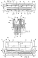
- FIG. 1 An electrical connector system constructed in accordance with the present invention is generally shown in Figure 1.
- the connector system is seen to include two major components.
- plug 10 and receptacle 12 will find particular use as terminators for terminating components containing multiple electrical conductors, i.e. cables or traces on circuit boards. Due to the relatively large number of electrical conductors now forming transmission cables, such conductors are typically splayed and connected to a printed circuit board (PCB).
- PCB printed circuit board
- a frame 18 includes a first crossbar or top wall 20, a second crossbar or bottom wall 22. a first plate 24, a second plate 26 (shown in Figures 3 and 4) and end walls 28 and 30. End walls 28 and 30 serve to maintain walls 20, 22, 24 and 26 in spaced relationship to one another. This arrangement of walls defines a number of channels which will be described in greater detail in relation to Figure 2.
- the walls of frame 18 are integrally formed. It is especially preferred to form such walls as a single metallic casting.
- Plug 10 also includes a number of insulated support structures. Only one support structure 32 is shown in Figure 1. Support structure 32 includes a forwardly extending finger 34. A plurality of contact elements 36 are disposed on finger 34 thereby defining a row of contact elements. As will be described below, each contact element includes a tail which extends rearwardly from frame 18 and is connected to PCB 14. Thus, each contact element 36 is connectable to one of the electrical conductors. Plug 10 is also shown to include plates 38 and 39, the purpose of which will be explained in greater detail below.
- receptacle 12 shown in Figure 1 Similar to plug 10, receptacle 12 includes a frame 40. Frame 40 is formed from base plate 42 and walls 44 and 46. Walls 44 and 46 are mounted to the base plate and extend towards the front of receptacle 12. Additional walls 48 and 50, shown more clearly in Figure 7, are also attached to base plate 42, however, these walls extend toward the rear of receptacle 12. As will be described in greater detail in relation to Figures 6 through 8, base plate 42 includes a number of passages, wherein such passages are located on both sides of wall 44 and on only one side of wall 46.
- receptacle 12 also includes a plurality of insulated support structures. Only structures 52, 54, 56, and 58 are shown. Each of these support structures is adapted to receive a plurality of contact springs, wherein the array of contact springs disposed within a support structure define a row of contact springs. As will be discussed in greater detail below, the contact springs extend rearwardly through base plate 42 for attachment to PCB 16. In this manner, each contact spring is connectable to one of the conductors for which receptacle 12 is serving as a terminator.
- frame 40 Similar to plug 10, it is preferred for walls 44, 46 and base plate 42 to be integrally formed. It is especially preferred for frame 40 to be formed as a single piece of metallic casting. In the embodiment shown in Figure 1, frame 40 also includes wall 62. It will be appreciated that high density connectors such as plug 10 and receptacle 12 will require alignment so that each contact element 36 will wipe against and make electrical contact with a single contact spring 60. To this end, various alignment structures are provided.
- frame 18 includes cylindrical bores 64 and 66. When plug 10 is inserted into receptacle 12, bore 64 slides on post 68 and bore 66 slides on post 70. In this manner, gross alignment is provided.
- Figure 1 also discloses slots 72 and 74 formed in end wall 30 and slots 76 and 78 formed in end wall 28. As plug 10 is inserted into receptacle 12, the ends of wall 44 slide within slots 72 and 76 while the ends of wall 46 slide within slots 74 and 78. In this manner, further alignment is provided.
- Still further alignment is provided by the sliding contact between the inside surface of wall 62 and the outside surface of wall 20 and the inside surface of walls 38 and 39 and the outside surface of wall 46. Additional alignment is provided by the center portion 80 of wall 44 passing in the gap 82 between walls 38 and 39. Additional alignment for plug 10 and receptacle 12 is described below. However, by means of the previously and below described alignment mechanisms, independent electrical connection is established between a single contact element and a single contact spring.
- frame 18 includes a number of passages 84, 86, 88, 90, 92 and 94.
- Insulated support structure 34 is positioned within passage 90.
- the other insulated support structures are positioned as follows: structure 98 is in passage 86; structure 96 is in passage 84; structure 100 is in passage 88; structure 102 is in passage 94; and structure 104 is in passage 92. It will be appreciated from Figure 2, and also from Figure 4, that support structures 96 and 98 are oriented within their respective passages, so that the wiper or forward portion of contact elements 36 face away from and are insulated from wall 20.
- support structures 102 and 104 are oriented within passages 94 and 92 so that the wiper portion of contact element 36 faces away from wall 22 and towards wall 38.
- support structures 34 and 100 positioned within passages 90 and 88, respectively, are oriented such that the wiper portion of contact element 36 faces away from wall 22 towards wall 20.
- insulated support structures 34 and 100 are integrally formed, being joined by a small web portion 106.
- Support structures 96 and 98 are integrally joined in a similar manner as are support structures 102 and 104.
- the ends of the support structures slide within guide slots 108 formed in end walls 28 and 30.
- slot 110 formed by joining two support structures with web portion 106 (shown in Figure 1) receives center wall 112, shown in Figure 3.
- center wall 112 is shown to include a number of posts 114, 116 and 118. As will be described in relation to Figure 6, when plug 10 and receptacle 12 are joined, posts 114-118 serve to provide further alignment and serve to provide additional electrical isolation between groups of contact elements.
- each contact element 36 is provided with a tail for mounting to a PCB (not shown).
- three rows of contact elements are provided by plug 10.
- the first row of contact elements consists of those arrays of contact elements mounted to support structures 96 and 98.
- the second row of contact elements consists of those arrays of contact elements mounted to support structures 34 and 100 and the third row of contact elements are those elements mounted to support structures 102 and 104.
- One of the features of the present invention is that each row of contact elements is electrically isolated from other rows of contact elements when frame 18 is connected to an electrical potential, preferably ground potential. This electrical isolation feature occurs for both the forward or wiper part of the contact element as well as the tail of the contact element.
- intermediate walls 24 and 26 extend rearwardly from frame 18 thereby electrically isolating a portion of the tails contained in the three rows of contact elements.
- an additional isolating member 120 is provided in order to complete the electrical isolation of the rows of contact elements.
- member or frame 120 is shown to include walls 122 and 124 which are maintained in spaced relation to each other by end walls 126 and 128.
- frame 120 serves to extend the electrical isolation between the tail portions of the contact element rows from the ends of walls 24 and 26 to the point at which the tails are mounted to a PCB. It is preferred for frame 120 to be integrally formed as a single metallic casting.
- plug 10 can be considered as having an insertion direction and a mounting direction.
- the insertion direction is that direction which plug 10 moves in order to be inserted into receptacle 12, i.e. a direction from frame 18 toward the front of plug 10.
- the mounting direction is that direction which permits plug 10 to be mounted to a printed circuit board, i.e. that direction which parallels the bores in the PCB in which the tails are to be mounted.
- an angle greater than 180° exists between the insertion direction and the mounting direction. Preferably this angle is approximately 270°.
- plug 10 is a right angle plug.
- a tail guide 130 is provided.
- Guide 130 is preferably formed from insulating material and has a plurality of bores passing there through. As will be seen in Figures 4 and 5, each tail portion of a contact element 36 passes through an individual bore in guide 130.
- key dimples 132 are provided. Key dimples 132 are designed to fit within appropriate recesses formed in frame 18.
- guide 130 includes a pair of channels through which walls 122 and 124 of member 120 extend. Thus, electrical isolation is further provided to the tails of contact elements 36 as they pass through guide 130.
- mounting bores 134 are provided in frame 18 for the mounting of assembled plug 10 to PCB 14.
- receptacle 12 includes a frame 40 having a base plate 42. Walls 44 and 46 are attached to baseplate 42 and extend forward towards the front of receptacle 12. As shown in Figure 6 and Figure 7, wall 44 includes several components, namely cap 140 and 142, support wall 144, end portions 146 and 148 and central portion 150. Preferably, the components of wall 44 are integrally formed as a part of the single piece, metallic receptacle casting referenced previously. Similarly, wall 46 includes cap members 152 and 154, support wall 156, center alignment post 80 and angle ends 158 and 160. As described previously, when plug 10 and receptacle 12 are joined, end members 146 and 148 will slide within slots 72 and 76 of plug 10, while angled ends 158 and 160 will move within slots 74 and 78 of plug 10.
- frame 40 has several passages formed therein.
- a passage is formed between wall 62 and support wall 144.
- a second passage is formed between support wall 144 and a fourth or intermediate wall 162.
- a third passage is formed between wall 162 and wall 156. It is noted that these passages extend across base plate 42. As shown in Figure 6, these passages are essentially divided in half by central wall 164.
- a number of insulated support structures (52, 54, 56, and 58) are inserted into these passages.
- the insulated support structures also include several components.
- the insulated support structures include a base member 164 from which extend fingers 166.
- Base members 164 and fingers 166 are adapted to receive a plurality of contact springs 60.
- a portion of contact spring 60 is embedded in base member 164.
- the forward end of the contact spring extends forward from base member 164 and is captured in the end portion of finger 166. It is noted that the end of spring number 60 is free to move within a pocket formed at the end of finger 166.
- Each contact spring 60 is also provided with a tail which extends rearwardly from base member 164.
- the contact springs are arranged in rows and that such rows are electrically isolated from one another.
- three rows of contact springs are provided, wherein one row is provided on one side of support wall 144 and oriented so that the curved end or spring portion of the contact spring faces wall 62.
- Another row of contact springs is provided on the other side of support wall 144 and oriented so that the spring portion faces wall 46.
- a third row of contact springs is provided adjacent support wall 156 and oriented so that the spring element is facing towards support wall 144.
- Support wall 144 and wall 162 serve to electrically isolate the contact springs when frame 40 is connected to an electrical potential, preferably ground potential.
- an isolation extension frame 167 is provided. As shown in Figure 7, frame 167 includes walls 168 and 170. In order to maintain electrical isolation: one edge of walls 168 and 170 is positioned proximate or in contact with the end of wall 144 and 162. Walls 168 and 170 can thus be considered as extending the isolation of walls 144 and 162. In an especially preferred embodiment, frame 167 is integrally formed as a metallic casting.
- receptacle 12 can be considered as having an insertion direction and a mounting direction.
- the insertion direction is that direction in which receptacle 12 receives plug 10, i.e., a direction from the front of receptacle 12 toward base plate 42.
- the mounting direction is that direction which permits receptacle 10 to be mounted to a printed circuit board, i.e. that direction which parallels the bores in the PCB in which the tails are to be mounted.
- an angle approximately equal to 180° exists between the insertion direction and the mounting direction while in Figure 8, an angle greater than 180° exists between the insertion direction and the mounting direction.
- this angle is approximately 270°.
- the receptacle shown in Figure 8 is a right angle receptacle.
- support wall 172 and wall 174 extend rearwardly from base plate 42 between the tails of the contact springs.
- Walls 172 and 174 generally correspond to support wall 144 and wall 162 shown in Figure 7.
- an isolation extension frame 175 is provided.
- Frame 175 includes walls 176 and 178 which are maintained in spaced relationship by end walls 180 and 182 (shown in Figure 9). It is especially preferred for extension member 175 to be integrally formed as a single metallic casting, similar to member 120 described in relation to Figures 4 and 5. Similarly, it is especially preferred for walls 168 and 170, shown in Figure 7, to form a part of a single extension member.
- wall 183 includes support walls 184 and 186.
- Wall 184 generally corresponds to wall 156 shown in Figure 7.
- a support wall corresponding to wall 186 is included in the embodiment of receptacle 12 shown in that Figure.
- a tail guide 190 is provided.
- Guide 190 is preferably formed from insulating material and has plurality of bores arranged in a particular pattern passing there through. As will be seen in Figures 8 and 9, each tail portion of a contact spring 60 passes through a individual bore in guide 190.
- key dimples 192 are provided. Dimples 192 are designed to fit within appropriate recesses formed in frame 40.
- guide 190 includes a pair of channels through which walls 176 and 178 pass. Thus electrical isolation is provided to the tails of contact spring 60 as they pass through guide 190.
- an electrical connector system 200 is shown to include a plug portion 210 and a receptacle portion 212.
- Plug portion 210 corresponds to plug 10 shown in Figure 4 and receptacle portion 212 corresponds to the embodiment of receptacle 12 shown in Figure 8.
- plug 210 includes three arrays of contact elements 214, 216 and 218.
- Plug 210 is also shown to include conductive walls 220 and 222.
- Receptacle 212 is shown to include three arrays of contact springs 224, 226 and 228.
- Receptacle 212 is also shown to include conductive walls 230 and 232 which separate the three arrays of contact springs.
- Plug 210 and receptacle 212 are adapted to mate with each other so that the arrays of contact elements 214, 216 and 218 form electrical connections with the arrays of contact springs 224, 226 and 228.
- conductive walls 220, 232, 222 and 230 are sandwiched with contact elements and contact springs disposed therebetween, thereby reducing crosstalk between adjacent arrays.
- conductive wall 232 extends to within a closer predetermined distance with conductive wall 234.
- a similar arrangement exists between conductive wall 222 and wall 236. The close proximity of the ends of these walls to one another forms a so-called "choke" joint, explained in greater detail in U.S. Patent Nos. 5,057,028 and 5,169,324 (Re. 35,508).
Landscapes
- Details Of Connecting Devices For Male And Female Coupling (AREA)
- Coupling Device And Connection With Printed Circuit (AREA)
Abstract
Description
Claims (20)
- An electrical plug for terminating multiple electrical conductors, said plug comprising:a frame, said frame comprising first and second crossbars, a first plate, a second plate and a plurality of walls maintaining said first and second crossbars and said first and second plates in spaced relationship, wherein said first plate is located closer to said second crossbar than to said first crossbar and wherein said second plate is located closer to said first crossbar than to said second crossbar, wherein said arrangement of crossbars and plates define first, second and third channels and wherein said frame is connectable to a predetermined electrical potential;first, second and third insulated support structures having forwardly extending fingers thereon, each of the fingers being received in one of said channels; anda plurality of contact elements being disposed on each of the fingers, thereby defining a row, each of the contact elements being connectable to one of the conductors, so that said plug provides first second and third rows of contact elements.
- An electrical plug for terminating multiple electrical conductors, said plug comprising:a frame comprising a top wall, a bottom wall, first and second intermediate walls, a center wall and end walls, wherein said end walls maintain said top, bottom, and intermediate walls in spaced relationship, wherein said arrangement of walls defines first, second and third channels and wherein said frame is connectable to an electrical potential;first, second and third insulated support structures having forwardly extending fingers thereon, each of the fingers being received in one of said first, second and third channels; anda plurality of contact elements being disposed on each of the fingers, thereby defining a row, each of the contact elements being connectable to one of the conductors, so that said plug provides first, second and third rows of contact elements.
- The plug of claim 2, wherein said walls are integrally formed.
- The plug of claim 3, wherein said frame comprises a metallic casting.
- The plug of claim 2, wherein said contact elements comprise tails for mounting on a printed circuit board.
- The plug of claim 5, further comprising an extension member, wherein said extension member is located proximate said first and second intermediate walls, so that said intermediate walls are electrically extended thereby.
- The plug of claim 6, wherein said extension member comprises first and second side walls and end walls, wherein one edge of each of said first and second side walls is positioned proximate said first and second intermediate walls.
- The plug of claim 5, further comprising a tail guide formed from insulating material, said tail guide having a plurality of bores passing therethrough, wherein said tails pass through said bores.
- The plug of claim 2, wherein said contact elements comprise a wiper portion and a tail portion, wherein said wiper and tail portions define an angle therebetween; in particular wherein said contact elements include a bend so that said wiper and tail portions are at an angle greater than 180 degrees to one another; and particularly wherein said angle is 270 degrees.
- An electrical receptacle for terminating multiple electrical conductors, said receptacle comprising:a frame formed of a base plate, first and second walls mounted to said base plate and extending toward the front of said receptacle, and third and fourth walls mounted to said base plate and extending toward the rear of said receptacle, said base plate having a number of passages therethrough, wherein said passages are located on both sides of said first wall;a plurality of insulated support structures adapted to receive a plurality contact springs therein, said contact support structures being positioned in said passages; anda plurality of contact springs being disposed in each of the support structures, each of the contact springs being connectable to one of the conductors, so that when said support structures are positioned in said passages, said receptacle provides first, second and third rows of contact springs.
- The receptacle of claim 10, wherein said walls are integrally formed; particularly wherein said frame comprises a metallic casting.
- The receptacle of claim 10, wherein said contact elements comprise tails for mounting on a printed circuit board.
- The receptacle of claim 12, wherein said third and fourth walls are located between said passages so that said tails extending from said first, second and third row of contact springs are divided by said third and fourth walls; particularly wherein said base plate further comprises end walls and wherein said third and fourth walls extend a sufficient distance toward said end walls as to be electrically connected thereto.
- The receptacle of claim 12, wherein said receptacle further comprises a second base plate and wherein said third and fourth walls are formed on said second base plate.
- The receptacle of claim 12, further comprising an extension member, wherein said extension member is located proximate said third and fourth walls, so that said third and fourth walls are electrically extended thereby; particularly wherein said extension member comprises first and second side walls and end walls, wherein one edge of each of said first and second side walls is positioned proximate said third and fourth walls.
- The receptacle of claim 12, further comprising a tail guide formed from insulating material, said tail guide having a plurality of bores passing therethrough, wherein said tails pass through said bores.
- The receptacle of claim 10, wherein said contact springs comprise a wiper portion and a tail portion, wherein said wiper and tail portions define an angle therebetween; in particular wherein said contact spring include a bend so that said wiper and tail portions are at an angle greater than 180 degrees to one another; and particularly wherein said angle is 270 degrees.
- An electrical connector system, comprising:a first connector having three arrays of contact conductive walls separating said three arrays of contact elements;a second connector having three arrays of contact elements and third and fourth conductive walls separating said three arrays of contact elements; andsaid second connector adapted to mate with said first connector so that said contact elements of said first and second connectors form electrical connections therebetween and so that said conductive walls are brought to within a predetermined distance from each other thereby reducing crosstalk between adjacent arrays of contact elements.
- The system of claim 18, wherein said first connector is a receptacle and said second connector is a plug; or wherein said first connector is a receptacle comprising:an insulative contact block for supporting at least a portion of an array of said contact elements;a conductive frame in which said insulative contact block is received; and said first conductive plate being integrally formed with said conductive frame.
- In a terminator for multiple electrical conductors of the type havinga first ground structure formed of a baseplate with a first plurality of walls thereon co-operating to define a predetermined number of channels arranged in side-by-side relationship;a number of insulated support structures having forwardly extending fingers formed thereon, each of the support structures being received in one of the channels; andelectrical contact elements being disposed on each of the fingers, each of the contact elements having a tail extending rearwardly from said ground structure, whereby a group of tails extends rearwardly from each of said support structures, so that, in use, said ground structure is connectable to a predetermined electrical potential whereby the electrical contact elements are electrically isolated from each other;the improvement comprising;a second ground structure formed of a second baseplate with a second plurality of walls thereon co-operating to define a passage, wherein said second ground structure is positioned so that at least one of said groups of tails passes through said passage and positioned so that said second plurality of walls electrically co-operates with said first plurality, whereby, said group of tails passing through said passage are electrically isolated from the other tails.
Applications Claiming Priority (2)
| Application Number | Priority Date | Filing Date | Title |
|---|---|---|---|
| US932407 | 1997-09-17 | ||
| US08/932,407 US5919063A (en) | 1997-09-17 | 1997-09-17 | Three row plug and receptacle connectors with ground shield |
Publications (3)
| Publication Number | Publication Date |
|---|---|
| EP0903816A2 true EP0903816A2 (en) | 1999-03-24 |
| EP0903816A3 EP0903816A3 (en) | 2001-01-24 |
| EP0903816B1 EP0903816B1 (en) | 2008-07-16 |
Family
ID=25462258
Family Applications (1)
| Application Number | Title | Priority Date | Filing Date |
|---|---|---|---|
| EP98117591A Expired - Lifetime EP0903816B1 (en) | 1997-09-17 | 1998-09-16 | Three row plug and receptacle connectors with ground shield |
Country Status (5)
| Country | Link |
|---|---|
| US (1) | US5919063A (en) |
| EP (1) | EP0903816B1 (en) |
| JP (1) | JPH11149961A (en) |
| DE (1) | DE69839718D1 (en) |
| TW (1) | TW404579U (en) |
Cited By (14)
| Publication number | Priority date | Publication date | Assignee | Title |
|---|---|---|---|---|
| WO2002049156A3 (en) * | 2000-11-08 | 2002-08-15 | Molex Inc | Mating system for electrical connectors |
| US11444397B2 (en) | 2015-07-07 | 2022-09-13 | Amphenol Fci Asia Pte. Ltd. | Electrical connector with cavity between terminals |
| US11469554B2 (en) | 2020-01-27 | 2022-10-11 | Fci Usa Llc | High speed, high density direct mate orthogonal connector |
| CN115425435A (en) * | 2022-08-11 | 2022-12-02 | 顺科智连技术股份有限公司 | Busbar connector and composite busbar |
| US11522310B2 (en) | 2012-08-22 | 2022-12-06 | Amphenol Corporation | High-frequency electrical connector |
| US11539171B2 (en) | 2016-08-23 | 2022-12-27 | Amphenol Corporation | Connector configurable for high performance |
| US11715914B2 (en) | 2014-01-22 | 2023-08-01 | Amphenol Corporation | High speed, high density electrical connector with shielded signal paths |
| US11757215B2 (en) | 2018-09-26 | 2023-09-12 | Amphenol East Asia Electronic Technology (Shenzhen) Co., Ltd. | High speed electrical connector and printed circuit board thereof |
| US11757224B2 (en) | 2010-05-07 | 2023-09-12 | Amphenol Corporation | High performance cable connector |
| US11799246B2 (en) | 2020-01-27 | 2023-10-24 | Fci Usa Llc | High speed connector |
| US11817655B2 (en) | 2020-09-25 | 2023-11-14 | Amphenol Commercial Products (Chengdu) Co., Ltd. | Compact, high speed electrical connector |
| US11942716B2 (en) | 2020-09-22 | 2024-03-26 | Amphenol Commercial Products (Chengdu) Co., Ltd. | High speed electrical connector |
| US12300920B2 (en) | 2021-08-13 | 2025-05-13 | Amphenol Commercial Products (Chengdu) Co., Ltd. | High performance card edge connector for high bandwidth transmission |
| US12300936B2 (en) | 2019-02-19 | 2025-05-13 | Amphenol Corporation | High speed connector |
Families Citing this family (23)
| Publication number | Priority date | Publication date | Assignee | Title |
|---|---|---|---|---|
| SG94711A1 (en) * | 1998-09-15 | 2003-03-18 | Molex Inc | Electrical connector for mounting on a printed circuit board and including a terminal tail aligner |
| TW421302U (en) * | 1998-12-18 | 2001-02-01 | Hon Hai Prec Ind Co Ltd | Electrical connector |
| USD451884S1 (en) | 2000-01-28 | 2001-12-11 | Japan Aviation Electronics Industry, Limited | Electrical connector |
| JP3688188B2 (en) * | 2000-07-19 | 2005-08-24 | ヒロセ電機株式会社 | Electrical connector with guide post |
| US7165994B2 (en) * | 2001-05-23 | 2007-01-23 | Samtec, Inc. | Electrical connector having a ground plane with independently configurable contacts |
| US6739884B2 (en) * | 2001-05-23 | 2004-05-25 | Samtec, Inc. | Electrical connector having a ground plane with independently configurable contacts |
| US6699068B2 (en) * | 2001-12-26 | 2004-03-02 | Hon Hai Precision Ind. Co., Ltd. | Stacked connector assembly |
| US6905367B2 (en) | 2002-07-16 | 2005-06-14 | Silicon Bandwidth, Inc. | Modular coaxial electrical interconnect system having a modular frame and electrically shielded signal paths and a method of making the same |
| US6705893B1 (en) * | 2002-09-04 | 2004-03-16 | Hon Hai Precision Ind. Co., Ltd. | Low profile cable connector assembly with multi-pitch contacts |
| JP2004319257A (en) * | 2003-04-16 | 2004-11-11 | Japan Aviation Electronics Industry Ltd | Balanced transmission connector |
| US20050057907A1 (en) * | 2003-09-12 | 2005-03-17 | Hewlett-Packard Development Company, L.P. | Circuit board assembly |
| TWI246808B (en) * | 2004-06-11 | 2006-01-01 | Hon Hai Prec Ind Co Ltd | Electrical connector |
| TW200849747A (en) * | 2007-06-15 | 2008-12-16 | Transcend Information Inc | USB connector device, connector module and manufacturing method |
| JP5590952B2 (en) * | 2010-04-15 | 2014-09-17 | 日本航空電子工業株式会社 | Board with connector |
| JP2012099454A (en) * | 2010-10-08 | 2012-05-24 | Sony Corp | Portable information processing device |
| US8430689B2 (en) * | 2011-07-22 | 2013-04-30 | Tyco Electronics Corporation | Electrical connector |
| US9548562B1 (en) * | 2015-09-22 | 2017-01-17 | Lenovo Enterprise Solutions (Singapore) Pte. Ltd. | Mid-plane connector configuration |
| TWI828624B (en) | 2017-06-13 | 2024-01-11 | 美商山姆科技公司 | Electrical connector system and method using the same |
| CN111095686B (en) | 2017-07-21 | 2023-02-03 | 申泰公司 | Electrical connector with latch |
| USD964291S1 (en) | 2017-07-21 | 2022-09-20 | Samtec, Inc. | Electrical connector |
| EP3701594A4 (en) | 2017-10-24 | 2021-07-21 | Samtec Inc. | RIGHT ANGLE ELECTRICAL CONNECTOR AND ELECTRICAL CONTACTS FOR A RIGHT ANGLE CONNECTOR |
| USD896183S1 (en) | 2018-01-08 | 2020-09-15 | Samtec, Inc. | Electrical cable connector |
| US20250079735A1 (en) * | 2023-09-05 | 2025-03-06 | Foxconn (Kunshan) Computer Connector Co., Ltd. | Electrical connector assembly with improved mating interfaces |
Family Cites Families (16)
| Publication number | Priority date | Publication date | Assignee | Title |
|---|---|---|---|---|
| US32691A (en) * | 1861-07-02 | Stove | ||
| US35508A (en) * | 1862-06-10 | Improvement in pumps | ||
| USRE32691E (en) | 1982-08-23 | 1988-06-07 | Amp Incorporated | High speed modular connector for printed circuit boards |
| US4571014A (en) * | 1984-05-02 | 1986-02-18 | At&T Bell Laboratories | High frequency modular connector |
| US5057028A (en) | 1986-11-18 | 1991-10-15 | E. I. Du Pont De Nemours And Company | Receptacle having a nosepeice to receive cantilevered spring contacts |
| US4824383A (en) * | 1986-11-18 | 1989-04-25 | E. I. Du Pont De Nemours And Company | Terminator and corresponding receptacle for multiple electrical conductors |
| JPH0741109Y2 (en) * | 1990-09-17 | 1995-09-20 | ヒロセ電機株式会社 | Electrical connector structure |
| US5169343A (en) * | 1990-11-29 | 1992-12-08 | E. I. Du Pont De Nemours And Company | Coax connector module |
| JP3182525B2 (en) * | 1991-07-03 | 2001-07-03 | タイコエレクトロニクスアンプ株式会社 | Discharge prevention type connector and connector shield device |
| US5174764A (en) * | 1991-12-20 | 1992-12-29 | Amp Incorporated | Connector assembly having surface mounted terminals |
| JP3108239B2 (en) * | 1993-02-19 | 2000-11-13 | 富士通株式会社 | Impedance matched electrical connector |
| FR2704696B1 (en) * | 1993-04-27 | 1996-05-31 | Rudolf Gorlich | Plug connector for printed circuit boards. |
| US5593311A (en) * | 1993-07-14 | 1997-01-14 | Thomas & Betts Corporation | Shielded compact data connector |
| US5344327A (en) * | 1993-07-22 | 1994-09-06 | Molex Incorporated | Electrical connectors |
| US5399105A (en) * | 1994-04-29 | 1995-03-21 | The Whitaker Corporation | Conductive shroud for electrical connectors |
| US5577936A (en) * | 1995-09-28 | 1996-11-26 | Berg Technology, Inc. | Wafer retention in an electrical receptacle |
-
1997
- 1997-09-17 US US08/932,407 patent/US5919063A/en not_active Expired - Fee Related
-
1998
- 1998-08-29 TW TW087214238U patent/TW404579U/en not_active IP Right Cessation
- 1998-09-16 EP EP98117591A patent/EP0903816B1/en not_active Expired - Lifetime
- 1998-09-16 DE DE69839718T patent/DE69839718D1/en not_active Expired - Fee Related
- 1998-09-17 JP JP26357798A patent/JPH11149961A/en not_active Withdrawn
Cited By (19)
| Publication number | Priority date | Publication date | Assignee | Title |
|---|---|---|---|---|
| WO2002049156A3 (en) * | 2000-11-08 | 2002-08-15 | Molex Inc | Mating system for electrical connectors |
| US11757224B2 (en) | 2010-05-07 | 2023-09-12 | Amphenol Corporation | High performance cable connector |
| US11901663B2 (en) | 2012-08-22 | 2024-02-13 | Amphenol Corporation | High-frequency electrical connector |
| US11522310B2 (en) | 2012-08-22 | 2022-12-06 | Amphenol Corporation | High-frequency electrical connector |
| US11715914B2 (en) | 2014-01-22 | 2023-08-01 | Amphenol Corporation | High speed, high density electrical connector with shielded signal paths |
| US11444397B2 (en) | 2015-07-07 | 2022-09-13 | Amphenol Fci Asia Pte. Ltd. | Electrical connector with cavity between terminals |
| US11955742B2 (en) | 2015-07-07 | 2024-04-09 | Amphenol Fci Asia Pte. Ltd. | Electrical connector with cavity between terminals |
| US12341301B2 (en) | 2016-08-23 | 2025-06-24 | Amphenol Corporation | Connector configurable for high performance |
| US11539171B2 (en) | 2016-08-23 | 2022-12-27 | Amphenol Corporation | Connector configurable for high performance |
| US11757215B2 (en) | 2018-09-26 | 2023-09-12 | Amphenol East Asia Electronic Technology (Shenzhen) Co., Ltd. | High speed electrical connector and printed circuit board thereof |
| US12300936B2 (en) | 2019-02-19 | 2025-05-13 | Amphenol Corporation | High speed connector |
| US11799246B2 (en) | 2020-01-27 | 2023-10-24 | Fci Usa Llc | High speed connector |
| US11817657B2 (en) | 2020-01-27 | 2023-11-14 | Fci Usa Llc | High speed, high density direct mate orthogonal connector |
| US11469553B2 (en) | 2020-01-27 | 2022-10-11 | Fci Usa Llc | High speed connector |
| US11469554B2 (en) | 2020-01-27 | 2022-10-11 | Fci Usa Llc | High speed, high density direct mate orthogonal connector |
| US11942716B2 (en) | 2020-09-22 | 2024-03-26 | Amphenol Commercial Products (Chengdu) Co., Ltd. | High speed electrical connector |
| US11817655B2 (en) | 2020-09-25 | 2023-11-14 | Amphenol Commercial Products (Chengdu) Co., Ltd. | Compact, high speed electrical connector |
| US12300920B2 (en) | 2021-08-13 | 2025-05-13 | Amphenol Commercial Products (Chengdu) Co., Ltd. | High performance card edge connector for high bandwidth transmission |
| CN115425435A (en) * | 2022-08-11 | 2022-12-02 | 顺科智连技术股份有限公司 | Busbar connector and composite busbar |
Also Published As
| Publication number | Publication date |
|---|---|
| EP0903816B1 (en) | 2008-07-16 |
| EP0903816A3 (en) | 2001-01-24 |
| US5919063A (en) | 1999-07-06 |
| TW404579U (en) | 2000-09-01 |
| JPH11149961A (en) | 1999-06-02 |
| DE69839718D1 (en) | 2008-08-28 |
Similar Documents
| Publication | Publication Date | Title |
|---|---|---|
| US5919063A (en) | Three row plug and receptacle connectors with ground shield | |
| US12149029B2 (en) | Electrical connector system | |
| US7175446B2 (en) | Electrical connector | |
| EP2274802B1 (en) | Board-to-board electrical connector | |
| CN102856692B (en) | Non-shielding, high-speed and low-crosstalk electric connector | |
| US7604490B2 (en) | Electrical connector with improved ground piece | |
| US6875031B1 (en) | Electrical connector with circuit board module | |
| JP4525959B2 (en) | Electrical connector having a housing for holding parallel circuit boards | |
| US6652319B1 (en) | High speed connector with matched impedance | |
| EP0924812B1 (en) | High density interstitial connector system | |
| US7040901B2 (en) | High-speed electrical connector | |
| US6347962B1 (en) | Connector assembly with multi-contact ground shields | |
| KR101021025B1 (en) | Electrical connector with contact plate | |
| US20220216652A1 (en) | Connector with improved shelding effect | |
| US6592407B2 (en) | High-speed card edge connector | |
| EP1732176A1 (en) | Electrical connector | |
| US20120058684A1 (en) | Low-cross-talk electrical connector | |
| US20160226193A1 (en) | Matched high-speed interconnector assembly | |
| US20240047907A1 (en) | Cable assembly for a cable connector module | |
| EP1652276A2 (en) | High-speed electrical connector | |
| CN201805026U (en) | Perpendicular connector | |
| KR100511537B1 (en) | Three rows of plug and receptacle connectors with earth shield |
Legal Events
| Date | Code | Title | Description |
|---|---|---|---|
| PUAI | Public reference made under article 153(3) epc to a published international application that has entered the european phase |
Free format text: ORIGINAL CODE: 0009012 |
|
| AK | Designated contracting states |
Kind code of ref document: A2 Designated state(s): DE FR GB IE |
|
| AX | Request for extension of the european patent |
Free format text: AL;LT;LV;MK;RO;SI |
|
| PUAL | Search report despatched |
Free format text: ORIGINAL CODE: 0009013 |
|
| AK | Designated contracting states |
Kind code of ref document: A3 Designated state(s): AT BE CH CY DE DK ES FI FR GB GR IE IT LI LU MC NL PT SE |
|
| AX | Request for extension of the european patent |
Free format text: AL;LT;LV;MK;RO;SI |
|
| RIC1 | Information provided on ipc code assigned before grant |
Free format text: 7H 01R 23/68 A, 7H 01R 13/658 B |
|
| 17P | Request for examination filed |
Effective date: 20010719 |
|
| AKX | Designation fees paid |
Free format text: DE FR GB IE |
|
| 17Q | First examination report despatched |
Effective date: 20030704 |
|
| GRAP | Despatch of communication of intention to grant a patent |
Free format text: ORIGINAL CODE: EPIDOSNIGR1 |
|
| RIC1 | Information provided on ipc code assigned before grant |
Ipc: H01R 13/658 20060101ALI20080102BHEP Ipc: H01R 12/00 20060101AFI20080102BHEP |
|
| GRAS | Grant fee paid |
Free format text: ORIGINAL CODE: EPIDOSNIGR3 |
|
| GRAA | (expected) grant |
Free format text: ORIGINAL CODE: 0009210 |
|
| RAP1 | Party data changed (applicant data changed or rights of an application transferred) |
Owner name: FCI |
|
| AK | Designated contracting states |
Kind code of ref document: B1 Designated state(s): DE FR GB IE |
|
| REG | Reference to a national code |
Ref country code: GB Ref legal event code: FG4D |
|
| REF | Corresponds to: |
Ref document number: 69839718 Country of ref document: DE Date of ref document: 20080828 Kind code of ref document: P |
|
| REG | Reference to a national code |
Ref country code: IE Ref legal event code: FG4D |
|
| PLBE | No opposition filed within time limit |
Free format text: ORIGINAL CODE: 0009261 |
|
| STAA | Information on the status of an ep patent application or granted ep patent |
Free format text: STATUS: NO OPPOSITION FILED WITHIN TIME LIMIT |
|
| 26N | No opposition filed |
Effective date: 20090417 |
|
| GBPC | Gb: european patent ceased through non-payment of renewal fee |
Effective date: 20081016 |
|
| REG | Reference to a national code |
Ref country code: FR Ref legal event code: ST Effective date: 20090529 |
|
| PG25 | Lapsed in a contracting state [announced via postgrant information from national office to epo] |
Ref country code: IE Free format text: LAPSE BECAUSE OF NON-PAYMENT OF DUE FEES Effective date: 20080916 |
|
| PG25 | Lapsed in a contracting state [announced via postgrant information from national office to epo] |
Ref country code: DE Free format text: LAPSE BECAUSE OF NON-PAYMENT OF DUE FEES Effective date: 20090401 |
|
| PG25 | Lapsed in a contracting state [announced via postgrant information from national office to epo] |
Ref country code: FR Free format text: LAPSE BECAUSE OF NON-PAYMENT OF DUE FEES Effective date: 20080930 |
|
| PG25 | Lapsed in a contracting state [announced via postgrant information from national office to epo] |
Ref country code: GB Free format text: LAPSE BECAUSE OF NON-PAYMENT OF DUE FEES Effective date: 20081016 |