EP0903688B1 - Detector of radio frequency signals for contactless IC card - Google Patents
Detector of radio frequency signals for contactless IC card Download PDFInfo
- Publication number
- EP0903688B1 EP0903688B1 EP98402303A EP98402303A EP0903688B1 EP 0903688 B1 EP0903688 B1 EP 0903688B1 EP 98402303 A EP98402303 A EP 98402303A EP 98402303 A EP98402303 A EP 98402303A EP 0903688 B1 EP0903688 B1 EP 0903688B1
- Authority
- EP
- European Patent Office
- Prior art keywords
- circuit
- detector
- phase
- output terminal
- signals
- Prior art date
- Legal status (The legal status is an assumption and is not a legal conclusion. Google has not performed a legal analysis and makes no representation as to the accuracy of the status listed.)
- Expired - Lifetime
Links
Images

Classifications
-
- G—PHYSICS
- G06—COMPUTING; CALCULATING OR COUNTING
- G06K—GRAPHICAL DATA READING; PRESENTATION OF DATA; RECORD CARRIERS; HANDLING RECORD CARRIERS
- G06K19/00—Record carriers for use with machines and with at least a part designed to carry digital markings
- G06K19/06—Record carriers for use with machines and with at least a part designed to carry digital markings characterised by the kind of the digital marking, e.g. shape, nature, code
- G06K19/067—Record carriers with conductive marks, printed circuits or semiconductor circuit elements, e.g. credit or identity cards also with resonating or responding marks without active components
- G06K19/07—Record carriers with conductive marks, printed circuits or semiconductor circuit elements, e.g. credit or identity cards also with resonating or responding marks without active components with integrated circuit chips
- G06K19/0723—Record carriers with conductive marks, printed circuits or semiconductor circuit elements, e.g. credit or identity cards also with resonating or responding marks without active components with integrated circuit chips the record carrier comprising an arrangement for non-contact communication, e.g. wireless communication circuits on transponder cards, non-contact smart cards or RFIDs
Definitions
- the invention relates to contactless smart cards in which the transmission of the binary data between the user device and the card is carried out at radio frequency and, more particularly, in such cards, a circuit for detecting such a transmission. in radiofrequency so as to accurately determine that it is such a type of transmission.
- Such smart cards work properly only if they recognize very quickly and with certainty that the user device communicates via radio frequency signals so as to get into the operating mode adapted to this type of signals.
- the comparator circuit 16 provides on its output terminal a V RF signal indicating the presence of radio frequency signals in binary amplitude modulation. It is this V RF signal which indicates to the microcontroller 50 that the signal transmitted to the card is of the radiofrequency type.
- EP-A-0 791 706 discloses a rectifying circuit. It comprises first and second transistors forming a first pair of transistors minimizing the voltage drop between the ground and the transponder substrate. Third and fourth transistors form a second pair of transistors minimizing the voltage drop between the maximum amplitude of the AC voltage and the output voltage of the rectifier circuit. The pairs of transistors are controlled by alternative input signals. A series control circuit decouples the first and second pairs of capacitive load transistors of the transponder circuit.
- the object of the invention is to provide a radio frequency signal detector for a smart card which determines with speed and certainty the presence of radiofrequency signals.
- the detector according to the invention uses the signals at the carrier frequency.
- the invention therefore relates to a radiofrequency signal presence detector for a contactless smart card according to the claims.
- the signals V AC1 and V AC0 can also be applied to other circuits of the smart card, in particular to a rectifying circuit 12 according to the diagram of FIG. 1 or to a circuit for generating data. the supply voltage of the smart card from the radiofrequency energy received.
- the output terminal of the circuit AND 32 may be connected directly to the microcontroller of the smart card to indicate that it is a transmission or not binary data by radio frequency or be connected to a first input terminal an AND circuit 34 whose other input terminal is connected to the output terminal of the comparator 16 of the diagram of FIG. 1.
- the phase-shift detector circuit 26 is in fact a phase opposition detector between the signals V AC1 and V AC0 which comprises (FIG. 5) an EXCLUSIVE OR 36 whose two input terminals respectively receive the signals V AC1 or V AC0 . It provides a signal when the two signals V AC1 or V AC0 are in phase opposition.
- a capacitor 38 is connected between the voltage power supply V DD and the output terminal of the circuit or EXCLUSIVE 36 to filter the effects of low amplitude phase changes between the signals V AC1 and V AC0 .
- the filtered signal is applied to a fitness circuit comprising for example two inverter circuits 46 and 48.
- the inverter circuit 40 and Schmit's Trigger are powered by the supply voltage V DD .
- the purpose of the inverting circuit is to transform the signal at the carrier frequency f into a square signal of amplitude V DD at the same frequency.
- the diode 42 prevents the discharge of the capacitor C 2 when the output terminal of the inverter circuit 40 is at ground potential.
- the capacitor C 2 and the resistor R 2 realize an integration circuit with discharge through the resistor R 2 .
- the voltage at the input terminal of the Schmit Trigger 44 increases as the frequency f of the signal increases. Consequently, its switching threshold and the values of the components C 2 and R 2 must be chosen so that the signals having a frequency greater than a certain value are detected and perform the switchover.
- the invention has been described with a detector comprising a phase shift detector circuit 26 and two radio frequency detectors 28 and 30 whose output signals are combined in the logic circuits 32,36.
Description
L'invention concerne les cartes à puce sans contact dans lesquelles la transmission des données binaires entre l'appareil utilisateur et la carte s'effectue à fréquence radio et, plus particulièrement, dans de telles cartes, un circuit de détection d'une telle transmission en radiofréquence de manière à déterminer avec exactitude qu'il s'agit d'un tel type de transmission.The invention relates to contactless smart cards in which the transmission of the binary data between the user device and the card is carried out at radio frequency and, more particularly, in such cards, a circuit for detecting such a transmission. in radiofrequency so as to accurately determine that it is such a type of transmission.
Dans les cartes à puce sans contact, il est connu de transmettre les données binaires de l'appareil utilisateur vers la carte par l'intermédiaire d'un signal à une fréquence porteuse, de 13,56 Mhz par exemple, qui est modulé en amplitude par les chiffres binaires du code à transmettre.In contactless smart cards, it is known to transmit the binary data of the user device to the card via a signal at a carrier frequency of 13.56 Mhz, for example, which is amplitude-modulated. by the binary digits of the code to be transmitted.
De telles cartes à puce ne fonctionnent correctement que si elles reconnaissent très rapidement et avec certitude que l'appareil utilisateur communique par l'intermédiaire de signaux radiofréquence de manière à se mettre sur le mode de fonctionnement adapté à ce type de signaux.Such smart cards work properly only if they recognize very quickly and with certainty that the user device communicates via radio frequency signals so as to get into the operating mode adapted to this type of signals.
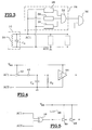
Cette reconnaissance s'effectue à l'aide d'un dispositif électronique du type de celui décrit par le schéma de la figure 1.This recognition is performed using an electronic device of the type described in the diagram of FIG.
Ce dispositif comprend :
- un circuit de
détection 10 des signaux radiofréquence constitué par un circuit résonant qui comprend une boucle d'antenne matérialisée par l'enroulement 20 et un condensateur C0 en parallèle. Cecircuit 10 fournit un signal VAC dont l'allure est donnée par le diagramme de la figure 2-a, - un circuit de redressement et
filtrage 12 constitué d'un pont à quatrediodes 22 suivi d'un condensateur C1 qui fournit un signal redressé double alternance VDC dont l'allure est donnée par le diagramme de la figure 2-b, - une
résistance 14, et - un circuit comparateur 16 qui compare les potentiels VDC et VDD aux bornes de la
résistance 14.
- a radio frequency
signal detecting circuit 10 consisting of a resonant circuit which comprises an antenna loop materialized by the winding 20 and a capacitor C 0 in parallel. Thiscircuit 10 provides a signal V AC , the appearance of which is given by the diagram of FIG. 2-a, - a rectifying and filtering
circuit 12 consisting of a four-diode bridge 22 followed by a capacitor C 1 which provides a full-wave rectified signal V DC whose gait is given by the diagram of FIG. 2-b, - a
resistor 14, and - a
comparator circuit 16 which compares the potentials V DC and V DD across theresistor 14.
Le circuit comparateur 16 fournit sur sa borne de sortie un signal VRF indiquant la présence de signaux radiofréquence en modulation binaire d'amplitude. C'est ce signal VRF qui indique au microcontrôleur 50 que le signal transmis à la carte est du type radiofréquence.The
Le document EP-A-0 791 706 décrit un circuit de redressement. Il comprend des premier et second transistors formant une première paire de transistors minimisant la chute de tension entre la masse et le substrat du transpondeur. Des troisième et quatrième transistors forment une seconde paire de transistors minimisant la chute de tension entre l'amplitude maximale de la tension alternative et la tension de sortie du circuit de redressement. Les paires de transistors sont commandées par des signaux d'entrée alternatifs. Un circuit de régulation série découple les première et deuxième paires de transistors de charges capacitives du circuit transpondeur.EP-A-0 791 706 discloses a rectifying circuit. It comprises first and second transistors forming a first pair of transistors minimizing the voltage drop between the ground and the transponder substrate. Third and fourth transistors form a second pair of transistors minimizing the voltage drop between the maximum amplitude of the AC voltage and the output voltage of the rectifier circuit. The pairs of transistors are controlled by alternative input signals. A series control circuit decouples the first and second pairs of capacitive load transistors of the transponder circuit.
L'invention a pour but de réaliser un détecteur de signaux radiofréquence pour carte à puce qui détermine avec rapidité et certitude la présence de signaux radiofréquence.The object of the invention is to provide a radio frequency signal detector for a smart card which determines with speed and certainty the presence of radiofrequency signals.
A cet effet, le détecteur selon l'invention utilise les signaux à la fréquence porteuse.For this purpose, the detector according to the invention uses the signals at the carrier frequency.
L'invention concerne donc un détecteur de présence de signaux radiofréquence pour carte à puce sans contact suivant les revendications.The invention therefore relates to a radiofrequency signal presence detector for a contactless smart card according to the claims.
D'autres caractéristiques et avantages de la présente invention apparaîtront à la lecture de la description suivante d'un exemple particulier de réalisation, ladite description étant faite en relation avec les dessins joints dans lesquels :
- la figure 1 est un schéma fonctionnel d'un détecteur de signaux radiofréquence selon l'art antérieur,
- les figures 2-a et 2-b sont des diagrammes de signaux à certains points du schéma de la figure 1,
- la figure 3 est un schéma fonctionnel d'un détecteur de signaux radiofréquence pour carte à puce selon l'invention,
- la figure 4 est un schéma de l'un des
circuits 28 ou 30 de la figure 3, et - la figure 5 est un schéma du détecteur de
phase 26 de la figure 3.
- FIG. 1 is a block diagram of a radiofrequency signal detector according to the prior art,
- FIGS. 2-a and 2-b are signal diagrams at certain points of the diagram of FIG. 1,
- FIG. 3 is a block diagram of a radio frequency signal detector for a smart card according to the invention,
- FIG. 4 is a diagram of one of the
circuits - FIG. 5 is a diagram of the
phase detector 26 of FIG.
Dans les différentes figures, les mêmes références indiquent des éléments identiques.In the different figures, the same references indicate identical elements.
Les figures 1 et 2 ont été décrites dans le préambule pour rappeler l'art antérieur et ne sont pas décrites à nouveau.Figures 1 and 2 have been described in the preamble to recall the prior art and are not described again.
Un détecteur selon l'invention est schématisé par les éléments de la figure 3. Il comprend :
- un circuit de
détection 10 du signal transmis par l'appareil utilisateur de la carte à puce (non représentée) qui fournit respectivement les signaux VAC1 et VAC0 aux extrémités AC1 et AC0 de l'enroulement 22, - un circuit de
détection 24 de la présence de signaux radiofréquence auquel sont appliqués les signaux VAC1 et VAC0.
- a
signal detection circuit 10 transmitted by the user device of the smart card (not shown) which respectively supplies the signals V AC1 and V AC0 at the ends AC1 and AC0 of thewinding 22, - a
detection circuit 24 for the presence of radiofrequency signals to which the signals V AC1 and V AC0 are applied.
Il est à noter que les signaux VAC1 et VAC0 peuvent être aussi appliqués à d'autres circuits de la carte à puce, notamment à un circuit de redressement 12 selon le schéma de la figure 1 ou encore à un circuit d'élaboration de la tension d'alimentation de la carte à puce à partir de l'énergie radiofréquence reçue.It should be noted that the signals V AC1 and V AC0 can also be applied to other circuits of the smart card, in particular to a rectifying
Le circuit de détection 24 comprend :
- un circuit détecteur de
déphasage 26 dont les deux bornes d'entrée sont connectées respectivement aux extrémités AC1 et AC0 de l'enroulement 20 et dont la borne de sortie est connectée à une première borne d'entrée des trois bornes d'entrée d'un circuit ET 32, - un
premier détecteur 28 de signaux radiofréquence dont la borne d'entrée est connectée à l'extrémité AC1 de l'enroulement 20 et dont la borne de sortie est connectée à la deuxième borne d'entrée du circuit ET 32, - un
deuxième détecteur 30 de signaux radiofréquence dont la borne d'entrée est connectée à l'extrémité AC0 de l'enroulement 20 et dont la borne de sortie est connectée à la troisième borne d'entrée du circuit ET 32, - le
circuit ET 32 dont les trois bornes d'entrée sont connectées comme indiqué ci-dessus et dont la borne de sortie fournit un signal de présence ou non d'un signal radiofréquence.
- a phase-
shift detector circuit 26 whose two input terminals are respectively connected to the ends AC1 and AC0 of thewinding 20 and whose output terminal is connected to a first input terminal of the three input terminals of aET circuit 32, - a first radio
frequency signal detector 28 whose input terminal is connected to the end AC1 of thewinding 20 and whose output terminal is connected to the second input terminal of theAND circuit 32, - a second radio
frequency signal detector 30 whose input terminal is connected to the end AC0 of thewinding 20 and whose output terminal is connected to the third input terminal of theAND circuit 32, - the
AND circuit 32 whose three input terminals are connected as indicated above and whose output terminal provides a presence signal or not of a radiofrequency signal.
La borne de sortie du circuit ET 32 peut être connectée directement au microcontrôleur de la carte à puce pour lui indiquer qu'il s'agit d'une transmission on non de données binaires par fréquence radio ou être connectée à une première borne d'entrée d'un circuit ET 34 dont l'autre borne d'entrée est connectée à la borne de sortie du comparateur 16 du schéma de la figure 1.The output terminal of the circuit AND 32 may be connected directly to the microcontroller of the smart card to indicate that it is a transmission or not binary data by radio frequency or be connected to a first input terminal an AND circuit 34 whose other input terminal is connected to the output terminal of the
Le circuit détecteur de déphasage 26 est en fait un détecteur d'opposition de phase entre les signaux VAC1 et VAC0 qui comprend (figure 5) un OU EXCLUSIF 36 dont les deux bornes d'entrée reçoivent respectivement les signaux VAC1 ou VAC0. Il fournit un signal lorsque les deux signaux VAC1 ou VAC0 sont en opposition de phase.The phase-
Un condensateur 38 est connecté entre la tension d'alimentation VDD et la borne de sortie du circuit ou EXCLUSIF 36 pour filtrer les effets des modifications de phase de faible amplitude entre les signaux VAC1 et VAC0.A
Le signal filtré est appliqué à un circuit de remise en forme comprenant par exemple deux circuits inverseurs 46 et 48.The filtered signal is applied to a fitness circuit comprising for example two
Chaque circuit détecteur 28 ou 30 comprend :
- un
circuit inverseur 40 dont la borne d'entrée est connectée à une extrémité AC1 ou AC0 de l'enroulement 20 selon le détecteur considéré, - une
diode 42 dont l'anode est connectée à la borne de sortie ducircuit inverseur 40, - un condensateur C2 dont une borne est connectée à la cathode de la
diode 42 et dont l'autre borne est connectée à la masse, - une résistance R2 montée en parallèle sur le condensateur C1 et,
- un circuit de basculement 44, du type connu sous le vocable "Trigger de Schmidt" dont la borne d'entrée est connectée au point commun de la résistance R1, du condensateur C1 et de cathode de la
diode 42.
- an
inverter circuit 40 whose input terminal is connected to an end AC1 or AC0 of the winding 20 according to the detector in question, - a
diode 42 whose anode is connected to the output terminal of theinverter circuit 40, - a capacitor C 2 , one terminal of which is connected to the cathode of the
diode 42 and whose other terminal is connected to ground, - a resistor R 2 connected in parallel with the capacitor C 1 and,
- a
tilt circuit 44, of the type known as the "Schmidt Trigger" whose input terminal is connected to the common point of the resistor R 1 , the capacitor C 1 and the cathode of thediode 42.
Le circuit inverseur 40 et le Trigger de Schmit sont alimentés par la tension d'alimentation VDD.The
Dans chaque circuit détecteur 28 ou 30 selon le schéma de la figure 4, le circuit inverseur a pour but de transformer le signal à la fréquence porteuse f en un signal carré d'amplitude VDD à la même fréquence. La diode 42 empêche la décharge du condensateur C2 lorsque la borne de sortie du circuit inverseur 40 est au potentiel de la masse. Le condensateur C2 et la résistance R2 réalisent un circuit d'intégration avec décharge au travers de la résistance R2.In each
La tension à la borne d'entrée du Trigger de Schmit 44 augmente au fur et à mesure que la fréquence f du signal augmente. En conséquence, son seuil de basculement et les valeurs des composants C2 et R2 doivent être choisis pour que les signaux ayant une fréquence supérieure à une certaine valeur soient détectés et réalisent le basculement.The voltage at the input terminal of the
L'invention a été décrite avec un détecteur comprenant un circuit détecteur de déphasage 26 et deux détecteurs radiofréquence 28 et 30 dont les signaux de sortie sont combinés dans les circuits logiques 32,36.The invention has been described with a detector comprising a phase
Cependant, un tel détecteur peut fonctionner en n'ayant que certains éléments :
- un seul détecteur 28
ou 30, - les deux seuls détecteurs 28
et 30, ce qui améliore la certitude de détection par rapport à un seul détecteur, - un seul détecteur 28
ou 30 avec le détecteur d'opposition de phase, - enfin, les deux détecteurs 28
et 30 et le détecteur d'opposition de phase comme décrits en relation avec la figure 3..
- a
single detector - the only two
detectors - a
single detector - finally, the two
detectors
En outre, les différents montages peuvent être combinés avec le circuit de l'art antérieur de la figure 1 comme indiqué ci-dessus.In addition, the various assemblies can be combined with the prior art circuit of FIG. 1 as indicated above.
Claims (3)
- A detector of the presence of radiofrequency signals for contactless chip cards, comprising a reception antenna winding (10) to detect the signals at the carrier frequency f transmitted by the user apparatus of the chip card, and at least one detection circuit (28, 30) to detect the presence of signals at the carrier frequency f, the input terminal of this detection circuit being connected to one end (AC1, AC0) of the antenna winding (10), characterized in that is further comprises:- a rectifying and filtering circuit (12) connected to the ends (AC1, AC0) of the antenna winding;- a phase-shift detector circuit (26) having two input terminals that are connected respectively to the ends (AC1, AC0) of the antenna winding (20), said phase-shift detector circuit providing, at its output terminal, a signal when the signals present at its input terminals are in phase opposition, and- an AND logic circuit (32) having at least two input terminals, one connected to the output terminal of the phase-shift detector circuit (26) and the other connected to the output terminal of one of the detection circuits (28 or 30).
- A detector according to claim 1, wherein said detection circuit (28 or 30) comprises:- an inverter circuit (40) whose input terminal is connected to one end (AC1, AC0) of the antenna winding (20),- a diode (42) whose anode is connected to the output terminal of the inverter circuit (40),- an integration circuit comprising a capacitor (C2) and a resistor (R2) that are parallel-connected, one of their common points being connected to the cathode of the diode (42), and- a flip-flop circuit (44) whose input terminal is connected to the cathode of the diode (42), said flip-flop circuit changing its state when the charging voltage attained by the capacitor (C2) is greater than a certain threshold.
- A detector according to claim 1 or 2, wherein the phase-shift detector circuit (26) comprises:- an EXCLUSIVE-OR circuit having two input terminals that are connected respectively to said ends (AC1, AC0) of the antenna winding (20), and- a capacitor (38) connected to the output terminal of the EXCLUSIVE-OR circuit.
Applications Claiming Priority (2)
| Application Number | Priority Date | Filing Date | Title |
|---|---|---|---|
| FR9711787 | 1997-09-23 | ||
| FR9711787A FR2768875B1 (en) | 1997-09-23 | 1997-09-23 | RADIO FREQUENCY SIGNAL DETECTOR FOR CONTACTLESS CHIP CARD |
Publications (2)
| Publication Number | Publication Date |
|---|---|
| EP0903688A1 EP0903688A1 (en) | 1999-03-24 |
| EP0903688B1 true EP0903688B1 (en) | 2006-05-24 |
Family
ID=9511349
Family Applications (1)
| Application Number | Title | Priority Date | Filing Date |
|---|---|---|---|
| EP98402303A Expired - Lifetime EP0903688B1 (en) | 1997-09-23 | 1998-09-17 | Detector of radio frequency signals for contactless IC card |
Country Status (5)
| Country | Link |
|---|---|
| US (1) | US6152373A (en) |
| EP (1) | EP0903688B1 (en) |
| JP (1) | JP3065586B2 (en) |
| DE (1) | DE69834607T2 (en) |
| FR (1) | FR2768875B1 (en) |
Families Citing this family (5)
| Publication number | Priority date | Publication date | Assignee | Title |
|---|---|---|---|---|
| US6837438B1 (en) * | 1998-10-30 | 2005-01-04 | Hitachi Maxell, Ltd. | Non-contact information medium and communication system utilizing the same |
| JP3824451B2 (en) * | 1999-07-29 | 2006-09-20 | 富士通株式会社 | Non-contact IC card presence / absence detection circuit |
| US6362972B1 (en) | 2000-04-13 | 2002-03-26 | Molex Incorporated | Contactless interconnection system |
| US6612852B1 (en) | 2000-04-13 | 2003-09-02 | Molex Incorporated | Contactless interconnection system |
| US7331979B2 (en) | 2003-06-04 | 2008-02-19 | Access Closure, Inc. | Apparatus and methods for sealing a vascular puncture |
Citations (1)
| Publication number | Priority date | Publication date | Assignee | Title |
|---|---|---|---|---|
| EP0791706A1 (en) * | 1996-01-31 | 1997-08-27 | Texas Instruments Deutschland Gmbh | Improvements in or relating to full-wave rectifiers |
Family Cites Families (6)
| Publication number | Priority date | Publication date | Assignee | Title |
|---|---|---|---|---|
| US3816708A (en) * | 1973-05-25 | 1974-06-11 | Proximity Devices | Electronic recognition and identification system |
| FR2662876B1 (en) * | 1990-05-29 | 1994-04-29 | Fontaine Sa | RADIOELECTRIC WAVE RECEIVER WITH INDUCTION LOOP AND EXTREMELY LOW CONSUMPTION, PARTICULARLY FOR REMOTE CONTROL. |
| US5533058A (en) * | 1994-03-10 | 1996-07-02 | Delco Electronics Corporation | Method and apparatus for low current RF signal detection |
| JPH0877318A (en) * | 1994-09-08 | 1996-03-22 | Toshiba Corp | Noncontact information recording medium |
| JPH0962816A (en) * | 1994-10-06 | 1997-03-07 | Mitsubishi Electric Corp | Non-contact ic card and non-contact ic card system including the same |
| JP3695833B2 (en) * | 1996-04-05 | 2005-09-14 | 株式会社ルネサステクノロジ | PLL circuit |
-
1997
- 1997-09-23 FR FR9711787A patent/FR2768875B1/en not_active Expired - Fee Related
-
1998
- 1998-09-17 EP EP98402303A patent/EP0903688B1/en not_active Expired - Lifetime
- 1998-09-17 DE DE69834607T patent/DE69834607T2/en not_active Expired - Lifetime
- 1998-09-18 US US09/157,060 patent/US6152373A/en not_active Expired - Lifetime
- 1998-09-24 JP JP10269355A patent/JP3065586B2/en not_active Expired - Lifetime
Patent Citations (1)
| Publication number | Priority date | Publication date | Assignee | Title |
|---|---|---|---|---|
| EP0791706A1 (en) * | 1996-01-31 | 1997-08-27 | Texas Instruments Deutschland Gmbh | Improvements in or relating to full-wave rectifiers |
Also Published As
| Publication number | Publication date |
|---|---|
| JP3065586B2 (en) | 2000-07-17 |
| FR2768875A1 (en) | 1999-03-26 |
| DE69834607D1 (en) | 2006-06-29 |
| EP0903688A1 (en) | 1999-03-24 |
| US6152373A (en) | 2000-11-28 |
| JPH11168416A (en) | 1999-06-22 |
| DE69834607T2 (en) | 2007-05-03 |
| FR2768875B1 (en) | 2000-06-02 |
Similar Documents
| Publication | Publication Date | Title |
|---|---|---|
| EP0903689A1 (en) | Demodulator for contactless chip card | |
| US8188787B2 (en) | Peak detector for detecting peaks in a modulated signal | |
| US6294953B1 (en) | High sensitivity demodulator for a radio tag and method | |
| US5889489A (en) | Diode receiver for radio frequency transponder | |
| EP1312032B1 (en) | High sensitivity reader for passive transponders | |
| JPH11174148A (en) | Electronic identification system | |
| WO2007129187A1 (en) | Method and device for transmitting data by charge modulation | |
| EP3001575B1 (en) | Method for managing the operation of an object capable of contactless communication with a reader, corresponding device and object | |
| EP1672388B1 (en) | Electromagnetic transponder without autonomous energy supply | |
| EP1496470A1 (en) | Dual-mode chip card | |
| FR2751148A1 (en) | DEMODULATOR OF AN ALTERNATIVE SIGNAL MODULE IN AMPLITUDE RECEIVED IN A COIL BY ELECTROMAGNETIC INDUCTION | |
| EP1043678B1 (en) | Duplex transmission in an electromagnetic transponder system | |
| EP2107694A1 (en) | Terminal for radiofrequency transmission-reception by means of inductive coupling | |
| EP0903688B1 (en) | Detector of radio frequency signals for contactless IC card | |
| EP0412884A1 (en) | Radio system for data transmission to a low cost passive terminal | |
| EP1043679B1 (en) | Reader having means for determining the distance between the reader and a transponder | |
| EP1269702B1 (en) | Demodulator of an amplitude-modulated alternating signal | |
| CA2191794C (en) | Power and modulation circuit for labels readable from a distance | |
| WO2004093341A1 (en) | Remote communication device by inductive coupling with multi-level modulation | |
| EP1665573A1 (en) | Portable object having multi-level demodulation and being inductively coupled to a fixed station | |
| KR100426303B1 (en) | Smart card | |
| FR2835119A1 (en) | WIDE DYNAMIC DEMODULATOR FOR CONTACTLESS CHIP CARDS OR LABELS | |
| US20030112062A1 (en) | Demodulation circuit and demodulation method | |
| FR2791491A1 (en) | REMOTE POWERING OF AN ELECTROMAGNETIC TRANSPONDER |
Legal Events
| Date | Code | Title | Description |
|---|---|---|---|
| PUAI | Public reference made under article 153(3) epc to a published international application that has entered the european phase |
Free format text: ORIGINAL CODE: 0009012 |
|
| AK | Designated contracting states |
Kind code of ref document: A1 Designated state(s): DE FR GB IT |
|
| AX | Request for extension of the european patent |
Free format text: AL;LT;LV;MK;RO;SI |
|
| 17P | Request for examination filed |
Effective date: 19990401 |
|
| AKX | Designation fees paid |
Free format text: DE FR GB IT |
|
| RAP1 | Party data changed (applicant data changed or rights of an application transferred) |
Owner name: STMICROELECTRONICS S.A. |
|
| 17Q | First examination report despatched |
Effective date: 20040220 |
|
| GRAP | Despatch of communication of intention to grant a patent |
Free format text: ORIGINAL CODE: EPIDOSNIGR1 |
|
| GRAS | Grant fee paid |
Free format text: ORIGINAL CODE: EPIDOSNIGR3 |
|
| GRAA | (expected) grant |
Free format text: ORIGINAL CODE: 0009210 |
|
| AK | Designated contracting states |
Kind code of ref document: B1 Designated state(s): DE FR GB IT |
|
| REG | Reference to a national code |
Ref country code: GB Ref legal event code: FG4D Free format text: NOT ENGLISH |
|
| REF | Corresponds to: |
Ref document number: 69834607 Country of ref document: DE Date of ref document: 20060629 Kind code of ref document: P |
|
| GBT | Gb: translation of ep patent filed (gb section 77(6)(a)/1977) |
Effective date: 20060822 |
|
| PLBE | No opposition filed within time limit |
Free format text: ORIGINAL CODE: 0009261 |
|
| STAA | Information on the status of an ep patent application or granted ep patent |
Free format text: STATUS: NO OPPOSITION FILED WITHIN TIME LIMIT |
|
| 26N | No opposition filed |
Effective date: 20070227 |
|
| PGFP | Annual fee paid to national office [announced via postgrant information from national office to epo] |
Ref country code: IT Payment date: 20070913 Year of fee payment: 10 |
|
| PGFP | Annual fee paid to national office [announced via postgrant information from national office to epo] |
Ref country code: GB Payment date: 20080827 Year of fee payment: 11 |
|
| PGFP | Annual fee paid to national office [announced via postgrant information from national office to epo] |
Ref country code: FR Payment date: 20080929 Year of fee payment: 11 |
|
| PG25 | Lapsed in a contracting state [announced via postgrant information from national office to epo] |
Ref country code: IT Free format text: LAPSE BECAUSE OF NON-PAYMENT OF DUE FEES Effective date: 20080917 |
|
| GBPC | Gb: european patent ceased through non-payment of renewal fee |
Effective date: 20090917 |
|
| REG | Reference to a national code |
Ref country code: FR Ref legal event code: ST Effective date: 20100531 |
|
| PG25 | Lapsed in a contracting state [announced via postgrant information from national office to epo] |
Ref country code: FR Free format text: LAPSE BECAUSE OF NON-PAYMENT OF DUE FEES Effective date: 20090930 |
|
| PG25 | Lapsed in a contracting state [announced via postgrant information from national office to epo] |
Ref country code: GB Free format text: LAPSE BECAUSE OF NON-PAYMENT OF DUE FEES Effective date: 20090917 |
|
| REG | Reference to a national code |
Ref country code: DE Ref legal event code: R082 Ref document number: 69834607 Country of ref document: DE Representative=s name: RAU, SCHNECK & HUEBNER PATENTANWAELTE RECHTSAN, DE |
|
| REG | Reference to a national code |
Ref country code: DE Ref legal event code: R082 Ref document number: 69834607 Country of ref document: DE Representative=s name: RAU, SCHNECK & HUEBNER PATENTANWAELTE RECHTSAN, DE Effective date: 20140704 Ref country code: DE Ref legal event code: R081 Ref document number: 69834607 Country of ref document: DE Owner name: MICRON TECHNOLOGY, INC., BOISE, US Free format text: FORMER OWNER: STMICROELECTRONICS S.A., MONTROUGE, FR Effective date: 20140704 |
|
| PGFP | Annual fee paid to national office [announced via postgrant information from national office to epo] |
Ref country code: DE Payment date: 20170912 Year of fee payment: 20 |
|
| REG | Reference to a national code |
Ref country code: DE Ref legal event code: R071 Ref document number: 69834607 Country of ref document: DE |