EP0903597A2 - Procédé d'inscription de réseaux de Bragg à réflexion dans guides optiques - Google Patents
Procédé d'inscription de réseaux de Bragg à réflexion dans guides optiques Download PDFInfo
- Publication number
- EP0903597A2 EP0903597A2 EP98307083A EP98307083A EP0903597A2 EP 0903597 A2 EP0903597 A2 EP 0903597A2 EP 98307083 A EP98307083 A EP 98307083A EP 98307083 A EP98307083 A EP 98307083A EP 0903597 A2 EP0903597 A2 EP 0903597A2
- Authority
- EP
- European Patent Office
- Prior art keywords
- grating
- waveguide
- writing
- diffraction
- bragg
- Prior art date
- Legal status (The legal status is an assumption and is not a legal conclusion. Google has not performed a legal analysis and makes no representation as to the accuracy of the status listed.)
- Granted
Links
Images


Classifications
-
- G—PHYSICS
- G03—PHOTOGRAPHY; CINEMATOGRAPHY; ANALOGOUS TECHNIQUES USING WAVES OTHER THAN OPTICAL WAVES; ELECTROGRAPHY; HOLOGRAPHY
- G03F—PHOTOMECHANICAL PRODUCTION OF TEXTURED OR PATTERNED SURFACES, e.g. FOR PRINTING, FOR PROCESSING OF SEMICONDUCTOR DEVICES; MATERIALS THEREFOR; ORIGINALS THEREFOR; APPARATUS SPECIALLY ADAPTED THEREFOR
- G03F7/00—Photomechanical, e.g. photolithographic, production of textured or patterned surfaces, e.g. printing surfaces; Materials therefor, e.g. comprising photoresists; Apparatus specially adapted therefor
- G03F7/70—Microphotolithographic exposure; Apparatus therefor
- G03F7/70058—Mask illumination systems
- G03F7/70066—Size and form of the illuminated area in the mask plane, e.g. reticle masking blades or blinds
-
- G—PHYSICS
- G02—OPTICS
- G02B—OPTICAL ELEMENTS, SYSTEMS OR APPARATUS
- G02B6/00—Light guides; Structural details of arrangements comprising light guides and other optical elements, e.g. couplings
- G02B6/02—Optical fibres with cladding with or without a coating
- G02B6/02057—Optical fibres with cladding with or without a coating comprising gratings
- G02B6/02076—Refractive index modulation gratings, e.g. Bragg gratings
- G02B6/02123—Refractive index modulation gratings, e.g. Bragg gratings characterised by the method of manufacture of the grating
- G02B6/02133—Refractive index modulation gratings, e.g. Bragg gratings characterised by the method of manufacture of the grating using beam interference
- G02B6/02138—Refractive index modulation gratings, e.g. Bragg gratings characterised by the method of manufacture of the grating using beam interference based on illuminating a phase mask
-
- G—PHYSICS
- G02—OPTICS
- G02B—OPTICAL ELEMENTS, SYSTEMS OR APPARATUS
- G02B6/00—Light guides; Structural details of arrangements comprising light guides and other optical elements, e.g. couplings
- G02B6/02—Optical fibres with cladding with or without a coating
- G02B6/02057—Optical fibres with cladding with or without a coating comprising gratings
- G02B6/02076—Refractive index modulation gratings, e.g. Bragg gratings
- G02B6/02123—Refractive index modulation gratings, e.g. Bragg gratings characterised by the method of manufacture of the grating
- G02B6/02152—Refractive index modulation gratings, e.g. Bragg gratings characterised by the method of manufacture of the grating involving moving the fibre or a manufacturing element, stretching of the fibre
Definitions
- This invention relates to the writing of Bragg reflection gratings in optical waveguides by exercise of the photorefractive effect in materials, such as germania doped silica.
- An early method of writing such gratings is described in United States Patent No. 4 474 427, this method involving directing intense ultra-violet light into one end of a length of optical waveguide having a reflector at the far end so that a standing wave is set up within the waveguide.
- a lateral method of writing such a grating was disclosed in United States Patent No. 4 725 110 in which a beam-splitter is used to divide a beam of ultra-violet light into two beams which are reflected in two mirrors to form and interference fringe pattern in the waveguide.
- a further alternative method sometimes known as the grating method, involves creating an equivalent fringe pattern close behind a diffraction grating illuminated with normally incident ultra-violet light, this method being described for instance in United States Patent No. 5 351 321.
- a phase grating is employed for this purpose, and the depth of the grating elements chosen for suppression of the zero order diffraction.
- the waveguide is located close behind the diffraction grating because it is here that the required fringe pattern, which is generated by interference between the +1 and -1 diffraction orders, is least disrupted by power diffracted into higher order modes.
- One advantage of this greater separation between the diffraction grating and the waveguide is that it enables a zero order beam stop to be located on the fused silica block to prevent any zero order light from reaching the fringe pattern generated by the interference between the +1 and -1 diffraction orders and thereby reducing the visibility of that fringe pattern.
- the present invention is concerned with the provision of a method of writing a Bragg reflection grating in an optical waveguide using a diffraction grating located at a sufficient distance from the waveguide as to make it readily possible to include aperture defining means to control the illumination of the waveguide so as to provide a high visibility fringe pattern, and at the same time to use separated portions of the diffraction grating for the generation of that fringe pattern.
- a method of writing a Bragg grating in a photosensitive optical waveguide by irradiating the waveguide (12) with an interference fringe pattern characterised in that said fringe pattern is generated by the passage of electromagnetic radiation in two spatially separated zones through a diffraction grating (11) oriented to have diffracting elements of the diffraction grating extending at an angle to the waveguide axis.
- a beam of intense ultra-violet light 10 is incident normally upon a diffraction grating 11 which is typically a phase grating whose depth is chosen to suppress the zero order diffraction of normally incident light.
- a diffraction grating 11 which is typically a phase grating whose depth is chosen to suppress the zero order diffraction of normally incident light.
- an optical fibre waveguide 12 Close behind the phase grating is located an optical fibre waveguide 12 whose axis extends transversely with respect to the direction of extent of the grating elements of the grating 11.
- the waveguide 12 is typically provided with a plastics protective coating 12a, a portion of which is removed to expose the bare fibre 12 in the region in which the Bragg reflection grating is to be written.
- At the centre of the optical fibre is its optical core 12b, the surface of which provides the waveguiding interface of the fibre.
- the light of beam 10 is concentrated upon this core by means of a cylindrical lens 13.
- the diffraction grating is divided into a number of beams of different diffraction order.
- Figure 1 just three of those beams are depicted, namely the -1 order diffraction beam 10a, the zero order diffraction beam 10b, and the +1 order diffraction beam 10c.
- the +1 order diffraction beam 10a Within the triangular area defined by the right-hand edge of the +1 order diffraction beam, the left-hand edge of the -1 order diffraction beam, and the diffraction grating itself there is complete overlap of the light of these two diffraction orders that thereby give rise to the potential of maximum fringe contrast.
- the light of beam 10 is divided into two substantially equal amplitude components 10' and 10" by means of a beam-splitter 20, these two components being incident, after reflection in mirrors 21 and 22, and optionally after passage through a cylindrical lens 23, normally upon the diffraction grating 11 in two spaced apart regions.
- This grating may be a uniform pitch grating or a chirped on. For the writing of a uniform pitch Bragg reflection grating it will be a uniform pitch grating.
- beam 10 of Figure 1 is divided into a number of beams of different diffraction order as the result of being incident normally upon the diffraction grating 11, the normally incident light of component beams 10' and 10" is similarly divided.
- Figure 2 also, just three of those beams are depicted for each component beam 10 and 10", namely the -1 order diffraction beams 10'a and 10"a, the zero order diffraction beam 10'b and 10"b, and the +1 order diffraction beams 10'c and 10"c.
- a field stop 24 is placed to intercept all the diffracted orders except for diffracted beams 10'c and 10"a, which pass through this field stop.
- the fibre 12 is located behind the field stop at the position where its core 12b lies where there is complete overlapping of the diffracted beams 10'c and 10"a.
- the cylindrical lens 23, if used, is employed to focus the light on to the core 12b of the fibre 12, and so performs an equivalent function to that performed by its counterpart lens 13 of Figure 1.
- the profiled surface of the phase grating 1 is liable to contamination leading to impairment of its performance. It is possible to remove this contamination by a special cleaning process, but this is rather time-consuming. It may be preferred therefore, since the fibre 12 is at some distance from this grating, to provide it with a silica cover slip 25 in order to protect its profiled surface from contamination, the exposed surface of the cover slip being capable of being cleaned much more readily and quickly.
- the apparatus of Figure 2 may be used for the writing of Bragg reflection gratings on a static basis, in which case further masking (not shown) may be employed for apodisation of the extremities of the written grating.
- the apparatus may be used for writing in a scanning mode, in which case there is ganged movement of the mirror 22 and the field stop 24 in the direction of axial extent of the fibre 12, such ganged movement being indicated by arrows 26.
- One of the problems liable to be encountered in the writing of long Bragg reflection gratings is the degradation of spectral performance introduced by the presence of stitch errors in the spacing of the diffracting elements of the diffraction grating employed to write that Bragg grating. These stitch errors are particularly liable to arise when the diffracting elements of the diffraction grating are themselves written in batches on a step-and-repeat basis for instance using E-beam lithographic techniques. Imperfections in the stepping process are liable to produce 'phase errors' of random magnitude between nearest neighbour diffraction elements of adjacent batches of elements.
- phase errors are translated with little modification from the diffraction grating to the Bragg reflection grating because relatively few diffraction elements of the diffraction grating contribute significantly to the writing of any individual element of the Bragg reflection grating.
- stitch errors in present in the diffraction grating 11 have less deleterious effect upon the spectral performance of Bragg reflectors written using the apparatus of Figure 2 than upon those written using the apparatus of Figure 1.
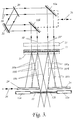
- Figure 3 shows a modified arrangement in which, in order to equalise the optical path length, the single mirror 22 has been replaced by a pair of mirrors 32a and 32b and the beam-splitter 20 and mirror 21 have been reoriented. In all other respects the components of the apparatus of Figure 3 are in essence identical with their counterparts in the apparatus of Figure 2.
Landscapes
- Physics & Mathematics (AREA)
- General Physics & Mathematics (AREA)
- Engineering & Computer Science (AREA)
- Manufacturing & Machinery (AREA)
- Optics & Photonics (AREA)
- Optical Fibers, Optical Fiber Cores, And Optical Fiber Bundles (AREA)
- Optical Integrated Circuits (AREA)
Applications Claiming Priority (2)
| Application Number | Priority Date | Filing Date | Title |
|---|---|---|---|
| GB9720135A GB2329484A (en) | 1997-09-22 | 1997-09-22 | Writing Bragg reflection gratings in optical waveguides |
| GB9720135 | 1997-09-22 |
Publications (3)
| Publication Number | Publication Date |
|---|---|
| EP0903597A2 true EP0903597A2 (fr) | 1999-03-24 |
| EP0903597A3 EP0903597A3 (fr) | 2000-05-10 |
| EP0903597B1 EP0903597B1 (fr) | 2002-11-13 |
Family
ID=10819463
Family Applications (1)
| Application Number | Title | Priority Date | Filing Date |
|---|---|---|---|
| EP98307083A Expired - Lifetime EP0903597B1 (fr) | 1997-09-22 | 1998-09-03 | Procédé d'inscription de réseaux de Bragg à réflexion dans guides optiques |
Country Status (5)
| Country | Link |
|---|---|
| US (1) | US6310996B1 (fr) |
| EP (1) | EP0903597B1 (fr) |
| CA (1) | CA2247744A1 (fr) |
| DE (1) | DE69809358T2 (fr) |
| GB (1) | GB2329484A (fr) |
Cited By (4)
| Publication number | Priority date | Publication date | Assignee | Title |
|---|---|---|---|---|
| WO2001075491A1 (fr) * | 2000-04-03 | 2001-10-11 | 3M Innovative Properties Company | Depot selectif de matiere sur un substrat selon un motif d'interference |
| US6391528B1 (en) | 2000-04-03 | 2002-05-21 | 3M Innovative Properties Company | Methods of making wire grid optical elements by preferential deposition of material on a substrate |
| WO2002044771A1 (fr) * | 2000-11-29 | 2002-06-06 | Fraunhofer-Gesellschaft zur Förderung der angewandten Forschung e.V. | Procede et dispositif de production d'un reseau de couplage pour un guide d'ondes |
| US6990272B2 (en) | 2001-07-26 | 2006-01-24 | Lxsix Photonics Inc. | Apparatus for generating an optical interference pattern |
Families Citing this family (24)
| Publication number | Priority date | Publication date | Assignee | Title |
|---|---|---|---|---|
| US6694075B1 (en) * | 1998-07-01 | 2004-02-17 | Corning Incorporated | Apodization of optical filters with multiple exposures of photosensitive media |
| CA2272008A1 (fr) * | 1999-05-11 | 2000-11-11 | Francois Trepanier | Dispositif et methode d'enregistrement de franges d'interference dans un support photosensible |
| US7246244B2 (en) * | 1999-05-14 | 2007-07-17 | Fusionarc, Inc. A Delaware Corporation | Identity verification method using a central biometric authority |
| CA2388519A1 (fr) * | 1999-09-29 | 2001-04-05 | Optical Technologies Italia S.P.A. | Procede de fabrication de laser a fibre |
| JP2001154040A (ja) * | 1999-11-25 | 2001-06-08 | Sumitomo Electric Ind Ltd | 光導波路型回折格子製造方法および装置 |
| US6842568B2 (en) | 1999-11-25 | 2005-01-11 | Sumitomo Electric Industries, Ltd. | Method of making diffraction grating device, diffraction grating device, and apparatus for making diffraction grating device |
| CA2394399A1 (fr) * | 1999-12-15 | 2001-06-21 | University Of Southampton | Interferometre : dispositif et procede |
| US6553163B2 (en) * | 2000-03-30 | 2003-04-22 | Corning, Incorporated | Method and apparatus for writing a Bragg grating in a waveguide |
| US6614959B1 (en) * | 2000-07-27 | 2003-09-02 | Ciena Corporation | Methods of writing apodized fiber gratings and associated apparatuses |
| US6836592B2 (en) * | 2000-11-20 | 2004-12-28 | Aculight Corporation | Method and apparatus for fiber Bragg grating production |
| US7184616B2 (en) * | 2000-11-20 | 2007-02-27 | Aculight Corporation | Method and apparatus for fiber Bragg grating production |
| US6898350B2 (en) * | 2001-01-18 | 2005-05-24 | General Dynamics Advanced Information Systems, Inc. | Interferometric focusing technique for forming taps in fibers |
| US6904201B1 (en) * | 2001-05-09 | 2005-06-07 | Intel Corporation | Phase-controlled fiber Bragg gratings and manufacturing methods |
| US6753118B2 (en) * | 2002-03-27 | 2004-06-22 | Fitel Usa Corp. | Optical grating fabrication process |
| US6801689B1 (en) * | 2002-04-30 | 2004-10-05 | Intel Corporation | Correcting the phase of waveguide bragg gratings |
| AUPS253202A0 (en) * | 2002-05-23 | 2002-06-13 | University Of Sydney, The | Interferometric grating writing methods and apparatus |
| US6847762B2 (en) * | 2002-07-02 | 2005-01-25 | Intel Corporation | Monitoring and correcting bragg gratings during their fabrication |
| US6904202B1 (en) * | 2002-07-31 | 2005-06-07 | Intel Corporation | Writing waveguides with an arbitrary Bragg wavelength |
| US7228034B2 (en) | 2003-11-03 | 2007-06-05 | Intel Corporation | Interference patterning |
| US7137299B2 (en) * | 2005-04-21 | 2006-11-21 | Northrop Grumman Corporation | Fiber optic accelerometer |
| KR100639038B1 (ko) * | 2005-05-18 | 2006-10-30 | 전남대학교산학협력단 | 브래그 격자 형성 장치 및 이에 이용되는 반사 유닛 |
| JP2009253209A (ja) * | 2008-04-10 | 2009-10-29 | Canon Inc | 露光装置及びデバイス製造方法 |
| NL2003950C2 (nl) * | 2009-12-11 | 2011-06-15 | Panalytical Bv | Werkwijze voor het vervaardigen van een meerlagenstructuur met een lateraal patroon voor toepassing in het xuv-golflengtegebied en volgens deze werkwijze vervaardigde bt- en lmag-structuren. |
| CN102436026A (zh) * | 2012-01-11 | 2012-05-02 | 西安盛佳光电有限公司 | 一次同时制作多根光纤光栅的方法 |
Family Cites Families (13)
| Publication number | Priority date | Publication date | Assignee | Title |
|---|---|---|---|---|
| US4474427A (en) | 1979-05-07 | 1984-10-02 | Canadian Patents & Development Limited | Optical fiber reflective filter |
| EP0191063B1 (fr) | 1984-08-13 | 1992-05-13 | United Technologies Corporation | Procede d'impression de reseaux dans des fibres optiques |
| US5351321A (en) | 1992-10-20 | 1994-09-27 | Elias Snitzer | Bragg grating made in optical waveguide |
| US5363239A (en) * | 1992-12-23 | 1994-11-08 | At&T Bell Laboratories | Method for forming spatially-varying distributed Bragg reflectors in optical media |
| GB9509874D0 (en) * | 1995-05-16 | 1995-07-12 | Univ Southampton | Optical waveguide grating |
| US5748814A (en) * | 1995-11-16 | 1998-05-05 | Institut National D'optique | Method for spatially controlling the period and amplitude of Bragg filters |
| DE19605062C1 (de) * | 1996-02-12 | 1997-08-28 | Univ Dresden Tech | Verfahren zur Erzeugung eines langen Bragg-Gitters in einer optischen Monomodefaser |
| US5668901A (en) * | 1996-02-14 | 1997-09-16 | Corning Incorporated | Low reflectivity fiber bragg grating with rectangular reflection function |
| CA2207226C (fr) * | 1996-06-10 | 2005-06-21 | Sumitomo Electric Industries, Ltd. | Reseau de diffraction integre a une fibre optique et procede de manufacture |
| US5745615A (en) * | 1996-10-11 | 1998-04-28 | Lucent Technologies Inc. | Method of making an optical fiber grating, and article made by the method |
| US5837169A (en) * | 1996-11-19 | 1998-11-17 | Northern Telecom Limited | Creation of bragg reflactive gratings in waveguides |
| US5945261A (en) * | 1996-11-19 | 1999-08-31 | Northern Telecom Limited | Creation of Bragg reflective gratings in waveguides |
| US5745617A (en) * | 1996-12-30 | 1998-04-28 | D-Star Technologies, Llc | Near-ultra-violet formation of refractive-index grating using reflective phase mask |
-
1997
- 1997-09-22 GB GB9720135A patent/GB2329484A/en not_active Withdrawn
-
1998
- 1998-01-29 US US09/015,675 patent/US6310996B1/en not_active Expired - Lifetime
- 1998-09-03 EP EP98307083A patent/EP0903597B1/fr not_active Expired - Lifetime
- 1998-09-03 DE DE69809358T patent/DE69809358T2/de not_active Expired - Fee Related
- 1998-09-21 CA CA002247744A patent/CA2247744A1/fr not_active Abandoned
Cited By (5)
| Publication number | Priority date | Publication date | Assignee | Title |
|---|---|---|---|---|
| WO2001075491A1 (fr) * | 2000-04-03 | 2001-10-11 | 3M Innovative Properties Company | Depot selectif de matiere sur un substrat selon un motif d'interference |
| US6391528B1 (en) | 2000-04-03 | 2002-05-21 | 3M Innovative Properties Company | Methods of making wire grid optical elements by preferential deposition of material on a substrate |
| WO2002044771A1 (fr) * | 2000-11-29 | 2002-06-06 | Fraunhofer-Gesellschaft zur Förderung der angewandten Forschung e.V. | Procede et dispositif de production d'un reseau de couplage pour un guide d'ondes |
| US6990272B2 (en) | 2001-07-26 | 2006-01-24 | Lxsix Photonics Inc. | Apparatus for generating an optical interference pattern |
| US7079729B2 (en) | 2001-07-26 | 2006-07-18 | Lxsix Photonics Inc. | Apparatus for generating an optical interference pattern |
Also Published As
| Publication number | Publication date |
|---|---|
| GB2329484A (en) | 1999-03-24 |
| EP0903597A3 (fr) | 2000-05-10 |
| GB9720135D0 (en) | 1997-11-19 |
| DE69809358T2 (de) | 2003-03-20 |
| US6310996B1 (en) | 2001-10-30 |
| DE69809358D1 (de) | 2002-12-19 |
| EP0903597B1 (fr) | 2002-11-13 |
| CA2247744A1 (fr) | 1999-03-22 |
Similar Documents
| Publication | Publication Date | Title |
|---|---|---|
| EP0903597B1 (fr) | Procédé d'inscription de réseaux de Bragg à réflexion dans guides optiques | |
| US5652818A (en) | Bragg gratings in waveguides and method of making same | |
| US5327515A (en) | Method for forming a Bragg grating in an optical medium | |
| EP0000810B1 (fr) | Méthode et appareil pour former des réseaux de diffraction focalisateurs pour l'optique intégrée | |
| USRE39865E1 (en) | Method of fabricating Bragg gratings using a silica glass phase grating mask and mask used by same | |
| US5367588A (en) | Method of fabricating Bragg gratings using a silica glass phase grating mask and mask used by same | |
| US5388173A (en) | Method and apparatus for forming aperiodic gratings in optical fibers | |
| EP0611972B1 (fr) | Méthode de fabrication de réflecteurs de Bragg distribués dans un milieu optique | |
| US6067391A (en) | Multiply periodic refractive index modulated optical filters | |
| AU731744B2 (en) | Phase mask with spatially variable diffraction efficiency | |
| US6549705B1 (en) | Fabrication of optical waveguide gratings | |
| AU706672B2 (en) | A method of forming a dispersing grating in an optical fiber | |
| JPH10319254A (ja) | 導波路中にブラッグ反射格子を形成する方法及びその方法によって形成されるブラッグ反射格子 | |
| KR20010080342A (ko) | 광유도 격자의 파장 조절 | |
| KR20010009101A (ko) | 광섬유격자 제작 장치 및 방법 | |
| US5694502A (en) | Bragg gratings in waveguides | |
| US5708739A (en) | Method and apparatus for photobleaching patterns in irradiated optical waveguides | |
| US7043121B2 (en) | Method and apparatus for writing apodized patterns | |
| GB2300932A (en) | Phase grating mask for making Bragg gratings in optical waveguides | |
| US6553163B2 (en) | Method and apparatus for writing a Bragg grating in a waveguide | |
| US6751381B1 (en) | Embodying amplitude information into phase masks | |
| KR960024698A (ko) | 조명계 및 주사형노광장치 | |
| JP2004538497A (ja) | 導波路にブラッググレーティングを書き込む方法及び装置 | |
| JPH08101322A (ja) | 透過型ファイバグレーティングフィルタの製造方法及びその装置 | |
| JPH11295541A (ja) | 導波路型回折格子の製造方法及び導波路型回折格子製造装置 |
Legal Events
| Date | Code | Title | Description |
|---|---|---|---|
| PUAI | Public reference made under article 153(3) epc to a published international application that has entered the european phase |
Free format text: ORIGINAL CODE: 0009012 |
|
| AK | Designated contracting states |
Kind code of ref document: A2 Designated state(s): DE FR GB IT |
|
| AX | Request for extension of the european patent |
Free format text: AL;LT;LV;MK;RO;SI |
|
| RAP3 | Party data changed (applicant data changed or rights of an application transferred) |
Owner name: NORTEL NETWORKS CORPORATION |
|
| PUAL | Search report despatched |
Free format text: ORIGINAL CODE: 0009013 |
|
| AK | Designated contracting states |
Kind code of ref document: A3 Designated state(s): AT BE CH CY DE DK ES FI FR GB GR IE IT LI LU MC NL PT SE |
|
| AX | Request for extension of the european patent |
Free format text: AL;LT;LV;MK;RO;SI |
|
| RIC1 | Information provided on ipc code assigned before grant |
Free format text: 7G 02B 6/16 A, 7G 02B 6/34 B |
|
| RAP1 | Party data changed (applicant data changed or rights of an application transferred) |
Owner name: NORTEL NETWORKS LIMITED |
|
| 17P | Request for examination filed |
Effective date: 20001110 |
|
| AKX | Designation fees paid |
Free format text: DE FR GB IT |
|
| 17Q | First examination report despatched |
Effective date: 20010215 |
|
| GRAG | Despatch of communication of intention to grant |
Free format text: ORIGINAL CODE: EPIDOS AGRA |
|
| GRAG | Despatch of communication of intention to grant |
Free format text: ORIGINAL CODE: EPIDOS AGRA |
|
| GRAH | Despatch of communication of intention to grant a patent |
Free format text: ORIGINAL CODE: EPIDOS IGRA |
|
| GRAH | Despatch of communication of intention to grant a patent |
Free format text: ORIGINAL CODE: EPIDOS IGRA |
|
| GRAA | (expected) grant |
Free format text: ORIGINAL CODE: 0009210 |
|
| AK | Designated contracting states |
Kind code of ref document: B1 Designated state(s): DE FR GB IT |
|
| PG25 | Lapsed in a contracting state [announced via postgrant information from national office to epo] |
Ref country code: IT Free format text: LAPSE BECAUSE OF FAILURE TO SUBMIT A TRANSLATION OF THE DESCRIPTION OR TO PAY THE FEE WITHIN THE PRESCRIBED TIME-LIMIT;WARNING: LAPSES OF ITALIAN PATENTS WITH EFFECTIVE DATE BEFORE 2007 MAY HAVE OCCURRED AT ANY TIME BEFORE 2007. THE CORRECT EFFECTIVE DATE MAY BE DIFFERENT FROM THE ONE RECORDED. Effective date: 20021113 |
|
| REG | Reference to a national code |
Ref country code: GB Ref legal event code: FG4D |
|
| REF | Corresponds to: |
Ref document number: 69809358 Country of ref document: DE Date of ref document: 20021219 |
|
| ET | Fr: translation filed | ||
| PLBE | No opposition filed within time limit |
Free format text: ORIGINAL CODE: 0009261 |
|
| STAA | Information on the status of an ep patent application or granted ep patent |
Free format text: STATUS: NO OPPOSITION FILED WITHIN TIME LIMIT |
|
| RAP2 | Party data changed (patent owner data changed or rights of a patent transferred) |
Owner name: NORTEL NETWORKS LIMITED |
|
| 26N | No opposition filed |
Effective date: 20030814 |
|
| PGFP | Annual fee paid to national office [announced via postgrant information from national office to epo] |
Ref country code: FR Payment date: 20040820 Year of fee payment: 7 |
|
| PGFP | Annual fee paid to national office [announced via postgrant information from national office to epo] |
Ref country code: GB Payment date: 20040901 Year of fee payment: 7 |
|
| PGFP | Annual fee paid to national office [announced via postgrant information from national office to epo] |
Ref country code: DE Payment date: 20040930 Year of fee payment: 7 |
|
| PG25 | Lapsed in a contracting state [announced via postgrant information from national office to epo] |
Ref country code: GB Free format text: LAPSE BECAUSE OF NON-PAYMENT OF DUE FEES Effective date: 20050903 |
|
| PG25 | Lapsed in a contracting state [announced via postgrant information from national office to epo] |
Ref country code: DE Free format text: LAPSE BECAUSE OF NON-PAYMENT OF DUE FEES Effective date: 20060401 |
|
| GBPC | Gb: european patent ceased through non-payment of renewal fee |
Effective date: 20050903 |
|
| PG25 | Lapsed in a contracting state [announced via postgrant information from national office to epo] |
Ref country code: FR Free format text: LAPSE BECAUSE OF NON-PAYMENT OF DUE FEES Effective date: 20060531 |
|
| REG | Reference to a national code |
Ref country code: FR Ref legal event code: ST Effective date: 20060531 |